DOI:
10.1039/C2RA20206A
(Paper)
RSC Adv., 2012,
2, 5277-5283
Organic Schottky diode based on conducting polymer–nanoclay composite
Received
5th February 2012
, Accepted 1st April 2012
First published on 2nd April 2012
Abstract
We report the fabrication and characterization of an electrochemically synthesized polycarbazole–organically modified nanoclay composite-based organic Schottky diode. The morphology of the nanocomposite is studied using scanning electron microscopy and high resolution transmission electron microscopy images, before fabrication of the diode. An intercalated, homogeneous nanocomposite is formed using an electrochemical method to get a uniform thin film directly onto the metal surface to create a better metal–organic junction, which plays a crucial role in the fabrication of a Schottky diode. The current density–voltage and capacitance–voltage characteristics of the Schottky diode are subsequently used for extracting electronic parameters of the device such as the ideality factor, barrier height, reverse saturation current, built-in potential, depletion width and doping concentration etc. Excellent rectifying behavior is observed with an ideality factor of 1.8. We also evaluate the photovoltaic characteristics of the device under illuminating conditions. Optical characterization of the device shows a high value of photo responsivity (8.22 × 10⁻⁴ A W−1) at −6 V.
Introduction
Conducting polymers and their derivatives have been intensively investigated and explored for their applications in electronic and optoelectronic devices, as well as their other applications like sensors, smart windows, soft actuators, artificial muscles, electromagnetic interference shielding, antistatic materials, and secondary batteries.1–6 Unfortunately, most of these applications have not yet reached the market and industry because of poor stability, mechanical properties and non-homogeneity of the conducting polymers and their composites. Nanocomposites, mainly with nanometals/metal oxides, nanoclay, carbon nanotubes, graphene, carbon fibers and fullerenes, get much more attention for their improvement of conducting polymers for their technological applications.7–15 Nanofillers not only stabilize the polymers but also affect their electronic properties, due to possible interactions of the pi orbitals of conjugated polymers providing ordering or alignment of polymer chains.
Clays are interesting host materials because of their availability, small particle size (>10 μm), low cost, template effect for polymer growth (due to their two-dimensional layered structure and negative charge) and well-known propensity for intercalation (charged galleries) with polymers.16–19 The polymer–clay nanocomposites were found to enhance the mechanical properties, gas barrier, thermal stability and fire-retardant properties of polymers.16–18 Conducting polymers encapsulated in two-dimensional layers of inorganic ceramics, or one-dimensional channels of organic hosts, offer interesting new perspectives. The constrained environment of an inorganic host should lead to a high degree of polymer ordering within the host, and this may have profound effects on polymer structure, properties, and electrical properties.20 Conducting polymer–clay nanocomposites have been reported with polyaniline, polypyrrole, poly(p-phenylene vinylene) and poly(3,4-ethylenedioxythiophene).21–24 Polycarbazole (PCz) is a relatively new conducting polymer with much better thermal and environmental stabilities than other conducting polymers. The electroactive and conducting form of PCz can be easily obtained by electrochemical polymerization.3,25–28 Polycarbazole and its derivatives have recently been studied for their use in light emitting diodes and photovoltaic devices.3,25,28 However, unsubstituted polycarbazole and its derivatives have hardly been explored for their applications and device fabrication.
These organic electronic and optoelectronic devices contain at least one conducting polymer–metal interface, and the performance of these devices strongly depends on this interface. Therefore, for improvement of these devices, it is necessary to understand not only the properties of the conducting polymers themselves, but also the interfacial electronic phenomena at the conducting polymer–metal interface. If a conducting polymer–metal contact forms the rectifying contact it is known as a Schottky diode. The fabrication and characterization of the Schottky diode barrier have been studied using various organic semiconductors and their derivatives. Grant et al. in 1981 fabricated the first Schottky diode based on undoped and lightly doped trans-polyacetylene with aluminum (Al) metal. However, the device characteristics degrade with time.29 Electronic properties of polypyrrole and their derivatives with metal junctions have been investigated in detail by several researchers.30–32 Polythiophene and its derivatives were also investigated for their use in Schottky diodes. The effect of regioregularity and electron withdrawing/donating substituents on the junction properties of a Schottky diode based on polythiophene has been studied.33–35 It was found that better performance of the Schottky diode could be achieved either with regioregular polymers with a short alkyl substituent, or by the presence of an electron withdrawing group. Polyaniline is not soluble in most of the organic solvents. However it was also investigated as an organic Schottky diode, due to its easy and cheap oxidative synthesis, thermal and environmental stability, and simple non-redox doping in acids. Polyaniline Schottky diodes have been prepared using electrochemical techniques36, 37 and less by casting techniques38 and they have found only moderate rectifying behavior. The electrical properties of the Schottky diode based on a polyaniline derivative and its composites have also been studied in detail.39–43 Most of the organic Schottky diodes showed poor diode properties with a high ideality factor, as well as poor thermal and mechanical stability. These problems may be overcome by introducing modified polymers including composites, and controlling the conducting polymer–metal interface. Therefore, it is necessary to explore new polymers and composites and control of the homogeneity and uniformity of the polymer films, including their morphology, for better electronic devices.
In this paper, we report for the first time the electronic and optical properties of an electrochemically formed PCz–clay nanocomposite Schottky diode, with a configuration of indium tin oxide (ITO) coated glass/PCz–clay/Al. The electrochemical polymerization technique is exploited less for the synthesis of nanocomposites, but we used this technique to get a homogeneous and uniform coating directly onto the substrate with a controlled morphology. Furthermore, it reduced the loss of materials (which occurs during spin coating) and improved the reproducibility and the ability to derive a homogenous thickness distribution over a large area. The device showed a much better performance in comparison to other similar devices.
Experimental section
Montmorillonite clay, surface-modified with 35–45 wt% dimethyl dialkyl (C14–C18) amine and carbazole monomer, was purchased from Aldrich Chemicals, USA, for the synthesis of the nanocomposite. Montmorillonite clay (0.1 wt% of the monomer) was dispersed in a dichloromethane solvent and sonicated for 10 min until a homogenous and stable distribution in the solvent was achieved. 60 mM carbazole and 0.1 M tetrabutyl ammonium perchlorate (TBAP), was added to this suspension. PCz–clay nanocomposite films were electrochemically polymerized (applying 1.3 V vs. Ag–AgCl reference electrode over ITO or metal plates) under ambient conditions by the same method as polycarbazole was formed in our previous papers.3,44 The formation of the nanocomposite was confirmed from scanning electron microscopy (GEMINI Zeiss SUPER TM 40 SEM) and high resolution transmission electron microscopy (Tecnai 30 G2 S-Twin electron microscope HRTEM) images. UV-vis spectra were recorded using a Lamda 25 Perkin Elmer spectrophotometer to confirm polymer formation and doping/dedoping states. ITO glass or metal electrodes coated with nanocomposites were properly washed and dried before device fabrication or other characterization. The sandwich cells of the Al/PCz–clay nanocomposite/ITO were fabricated by coating Al metal thin film using the thermal vacuum evaporation method. The Al/PCz–clay nanocomposite/ITO device was not sealed up from attack of moisture and oxygen, but kept in a vacuum desiccator for further characterization. The thickness of the nanocomposite was of the order of 400 nm and the thickness of the metal on top of the nanocomposite film was pre-adjusted to 80 nm in each case. Current density–voltage (J–V) and capacitance–voltage (C–V) measurements of ITO/PCz–clay/Al devices were carried out with a HP Semiconductor Parameter Analyzer (SPA), Hewlett Packard, USA make, Model No.−4145B and an LCR Meter, Hewlett Packard, Model-HP4284A, respectively, at room temperature (27 °C) in air under dark conditions (otherwise stated for illuminated conditions). X-ray diffraction (XRD) was performed using a Bruker AXS D8 Advance wide-angle X-ray diffractometer with Cu-Kα radiation and a graphite monochromator (wavelength, λ = 0.154 nm). The film of the polycarbazole–organically modified nanoclay composite in powder form was placed on a quartz sample holder at room temperature.
Results and discussion
The electrochemically formed nanocomposite is studied for its uniformity and morphology using SEM and HRTEM as shown in Fig. 1 and Fig. 2, respectively. The white flaky layers of clay are clearly shown in the SEM image. The morphology of the PCz–clay nanocomposite is distinct from that of the clay. The PCz–clay nanocomposite film exhibits a particularly dense and more compact morphology, which is distinct from the flaky morphology of the clay. The SEM images of the electrochemically polymerized PCz–clay nanocomposite show that the polymerization occurs mainly over the surfaces and probably between the clay layers. PCz modified the clay and formed a uniform composite. This is further supported by HRTEM images of the clay and the electrochemically polymerized PCz–clay nanocomposites. These clearly show the increment in d spacing (1.32 nm) of clay layers in the nanocomposites in comparison to pure clay, which was due to the polymerization of PCz between the clay layers. This may improve the electrical properties of the PCz–clay nanocomposite because of more ordered and dense structure, probably enhancing inter-chain electron hopping. The change in the d spacing of the clay is further supported by XRD as shown in Fig. 2. The 001 peak of the clay shifted to a lower wavelength on composite formation, indicating the opening of the clay layer and intercalation of PCz. ITO coated with a PCz–clay nanocomposite is used to fabricate the device by coating Al metal over the PCz–clay nanocomposite.
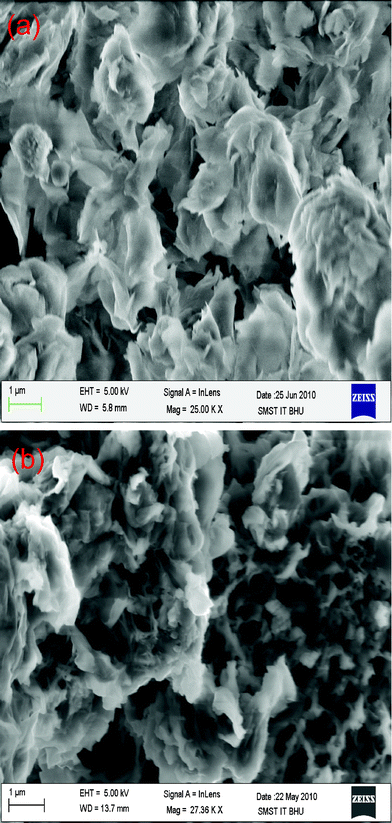 |
| | Fig. 1 SEM image of (a) clay, (b) PCz–clay nanocomposite. | |
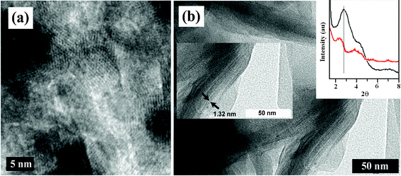 |
| | Fig. 2 HRTEM image of (a) clay, (b) PCz–clay nanocomposite and inset show the spacing of the clay layers and XRD of pure clay (black) and PCz–clay nanocomposite (red). | |
The electronic properties of the device Al/PCz–clay nanocomposite/ITO are investigated by current density–voltage (J–V) and capacitance–voltage (C–V) measurements at room temperature (27 °C) in air under dark conditions. The schematic structure of the device is shown in Fig. 3. The J–V characteristic shows good quality rectifying behavior of the Al/PCz–clay/ITO device as shown in Fig. 4. The departures of the current values from typical characteristics, at different applied voltages, for random samples taken from the four sets fabricated in the lab, are expressed in terms of standard deviation (shown by vertical lines at the data points on the J–V characteristics). According to the standard emission–diffusion theory, the dependence of current density on voltage for metal–semiconductor rectifying contacts is given by45
| |  | (1) |
| |  | (2) |
where
A* is the effective Richardson constant with
A* = 120 A cm
−2 K
−2,
J0 is the saturation current density in the absence of external bias,
T is the absolute temperature,
η is the diode quality factor (ideality factor),
k is the Boltzmann constant and
φB is the barrier height.
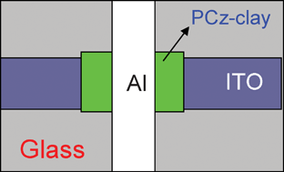 |
| | Fig. 3 Schematic structure of the Al/PCz–clay/ITO device. | |
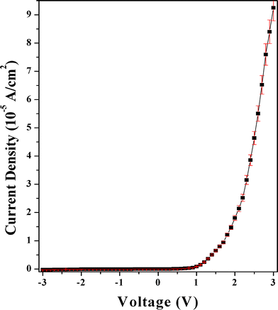 |
| | Fig. 4
J–V characteristics of the Al/PCz–clay/ITO device. | |
The ideality factor (η) and barrier height (φB) are obtained from the slope and reverse saturation current density, respectively. The value of the reverse saturation current density is obtained from the intercepts of ln(J) versus V at V = 0. The values of the ideality factor, barrier height and reverse saturation current density are listed in Table 1. The larger than unity value of the ideality factor is attributed to the inhomogeneity of the barrier . However, the ideality factor of the Al/PCz–clay/ITO device is better than the Al/PCz/ITO device.3 The ideality factor of this device is much better than those of other organic Schottky diodes reported earlier.31 The low value of J0 for the Al/PCz–clay/ITO device accounted for the larger depletion width (as confirmed from C–V measurements discussed later in this section), which reduces the possibility of tunneling at the interface. It is observed that the forward current also starts increasing sharply at a lower voltage in the Al/PCz–clay/ITO device in comparison to the Al/PCz/ITO device.3 The forward current is also larger in the Al/PCz–clay/ITO device in comparison to the Al/PCz/ITO device.3 However, the reverse saturation current density of the Al/PCz–clay/ITO device is nearly same as the Al/PCz/ITO device. The improvement in the electrical properties of the Al/PCz–clay/ITO device is mainly due to the presence of nano clay in the polymer matrix. The nano clay changed the morphology, because nano galleries provided the platform for growth of the polymer in a regular manner. The alignment of the polymer chains is much better in the nanocomposite. It has also been reported earlier by others for similar composites.16,17
Table 1 Device electrical parameters of Al/PCz–clay/ITO
| Device |
η
|
φ
B
(eV) |
J
0
(A cm−2) |
V
bi (V) |
NA (cm−3) |
Wd (nm) for applied voltage |
| 0 V |
−3 V |
| ITO/PCz–clay/Al |
1.83 |
0.85 |
5.34 × 10⁻¹⁰ |
0.78 |
1.76 × 10¹⁷ |
87.6 |
193 |
The charge transport mechanism of the Schottky diode can be understood by the log–log plot of J–V characteristics as shown in Fig. 5. The curve shows voltage dependence, followed by power law dependence at higher voltages. It is clear from Fig. 5 that the graph has three different linear regions (1, 2 and 3). The first region (voltages up to 0.5 V) exhibits an ohmic behavior. In the second region, up to 1.5 V, a square law region appears and charge transport is mainly governed by space charge limited current (SCLC) with an exponential distribution of traps in the band gap of the organic material.39 In the third region (at higher voltages), the slope of the curve decreases because the device approaches the trap filled limit, and behavior in this region is the same as in trap free SCLC.46 There are three linear different segments, and this behavior may be attributed to three different charge conduction mechanisms.
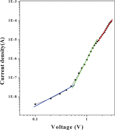 |
| | Fig. 5 The forward bias logJ–logV plot of the ITO/PCz–clay/Al device. | |
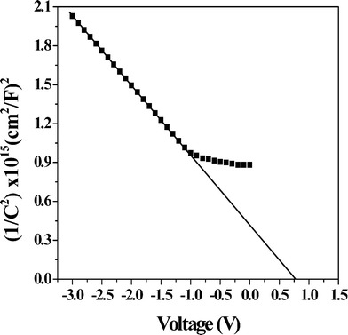
Fig. 6 shows the 1/C2–V characteristic of the Al/PCz–clay/ITO device, measured experimentally at 100 kHz and room temperature by LCR meter. The C–V relationship of the Schottky diode under bias can be expressed as30
| | 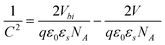 | (3) |
where
C is the junction capacitance of the Schottky diode per unit area,
V is the applied voltage,
ε0 is the free space permittivity,
Vbi is the built-in potential at zero bias,
εs is the dielectric constant of the material and
NA is the acceptor concentration in the depletion layer. The carrier concentration
NA is calculated from the slope of the linear portion of the plot of 1/
C2vs. V, and the built-in potential
Vbi is calculated by extrapolating the linear region of 1/
C2vs. V to cut the
V axis. The depletion layer width is expressed as
45| |  | (4) |
 |
| | Fig. 6 1/C2versus V characteristic of ITO/PCz–clay/Al device. | |
The variation in the depletion layer width with the applied voltage, as estimated on the basis of eqn (4), is shown in Fig. 7. The values of the built-in potential, acceptor concentration and depletion layer width are listed in Table 1, and these values are fairly similar to the Al/PCz/ITO device.3
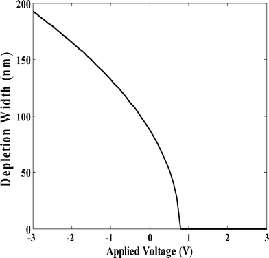 |
| | Fig. 7 The variation in depletion layer width with applied voltage. | |
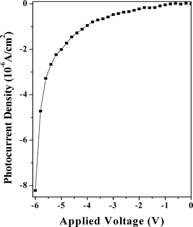
Fig. 8 depicts the reverse bias characteristics of the nanocomposite Schottky diode in the dark and under illumination of red light (λ = 650 nm, optical power = 10 mW cm−2) through the back side of the glass slide using an ILD (injection laser diode) unit with drive circuit from Benchmark (Model No. FOSM-D 600). The UV-vis spectrum of the PCz–clay nanocomposite, taken in tetrahydrofuran, does not show any significant change from the spectrum of the PCz polymer as shown in Fig. 9. The absorption peak at 341 nm (due to π–π* transitions of the conjugated chain), at 386 nm (due to polaron bonding level to the conduction band) and the broad hump at 600–750 nm (due to the bonding level to antibonding state of polaron) appeared for all the composites and the pure polymer. A broad peak at 650 nm in the nanocomposite was observed, similar to that obtained for pure PCz, and shown in the inset of Fig. 9. The variation in photocurrent density of the device with the applied voltage varying from 0 to −6.0 V is shown in Fig. 10. It is seen that for a given applied voltage there is a significant change in the value of the photo current, under the illumination of a 650 nm laser light source, which may be due to Schottky barrier modulation. The Schottky barrier modulation is induced by a local electric field. When the laser light is illuminated at the interface, some energetic electrons overcome the tunnel barrier at the interface and fall into metal electrodes, leaving holes in the film. This causes an electron–hole separation at the interface and thereby creates a local electric field. A high value of photocurrent and a low accompanying dark current of the fabricated device would make it attractive for use as a photodetector in an optical communication system operating in the visible region at 650 nm.
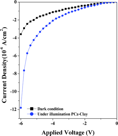 |
| | Fig. 8 Reverse bias J–V characteristics of Al/PCz–clay/ITO under illumination of light. | |
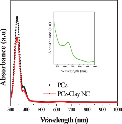 |
| | Fig. 9 UV-vis spectra of PCz and the PCz–clay nanocomposite, and the inset shows the UV-vis spectra of PCz–clay nanocomposite on a large scale. | |
 |
| | Fig. 10 Photocurrent density versus reverse voltage. | |
Conclusion
The electrochemically polymerized polycarbazole–clay nanocomposite films were used as semiconductor material for formation of Schottky junctions with a low-cost metal like Al. The current density–voltage (J–V) and capacitance–voltage (C–V) measurements were used for extraction of the diode performance parameters under dark conditions. The optical characterization of the device revealed a high value of responsivity (8.22 × 10⁻⁴ A W−1) at −6 V. It is anticipated that the presence of organic modified clay in the polymer matrix also enhances the mechanical and thermal stability of these devices. The electrical and optical measurements confirmed that the Schottky diode can be used as a flexible electronic and optoelectronic device.
Acknowledgements
Authors are thankful to Prof. A.C. Pandey, Allahabad University for providing HRTEM facilities and fruitful discussions. A. K. Singh is thankful to CSIR for financial support.
References
-
T. A. Skotheim, R. L. Elsenbaumer and J. R. Reynolds, Handbook of Conducting Polymers, M. Dekker, New York , 1998 Search PubMed.
- A. J. Heeger, Chem. Soc. Rev., 2010, 39, 2354 RSC.
- A. K. Singh, A. D. D. Dwivedi, P. Chakrabarti and R. Prakash, J. Appl. Phys., 2009, 105, 114506 CrossRef.
- B. Adhikari and S. Majumdar, Prog. Polym. Sci., 2004, 29, 699 CrossRef CAS.
- K. Yamato and K. Kaneto, Anal. Chim. Acta, 2006, 568, 133 CrossRef CAS.
- W. H. Meyer, Adv. Mater., 1998, 10, 439 CrossRef CAS.
- D. Shah, P. Maiti, E. Gunn, D. F. Schmidt, D. D. Jiang, C. A. Batt and E. R. Giannelis, Adv. Mater., 2004, 16, 1173 CrossRef CAS.
- E. Manias, Nat. Mater., 2007, 6, 9 CrossRef CAS.
- P. M. Ajayan, O. Stephan, C. Colliex and D. Trauth, Science, 1994, 265, 1212 CAS.
- H. Xin, F. S. Kim and S. A. Jenekhe, J. Am. Chem. Soc., 2008, 130, 5424 CrossRef CAS.
- W. Takashima, S. Kawamura and K. Kaneto, Electrochim. Acta, 2011, 56, 4603 CrossRef CAS.
- T. Morita, V. Singh, S. Oku, S. Nagamatsu, W. Takashima, S. Hayase and K. Kaneto, Jpn. J. Appl. Phys., 2010, 49, 041601 CrossRef.
- H. Pandey, V. Parashar, R. Parashar, R. Prakash, P. W. Ramteke and A. C. Pandey, Nanoscale, 2011, 3, 4104 RSC.
- A. K. Singh, P. Chakrabarti and R. Prakash, IEEE Electron Device Lett., 2011, 32, 593 CrossRef CAS.
- V. Parashar, K. Kumar, R. Prakash, S. K. Pandey and A. C. Pandey, J. Mater. Chem., 2011, 21, 6506 RSC.
- S. S. Ray and M. Okamoto, Prog. Polym. Sci., 2003, 28, 1539 CrossRef CAS.
- Z. Jinguo, E. Manias and A. Charles, J. Nanosci. Nanotechnol., 2008, 8, 1597 CrossRef.
- F. Hussain, M. Hojjati, M. Okamoto and R. E. Gorga, J. Compos. Mater., 2006, 40, 1511 CrossRef CAS.
- A. K. Singh, L. Joshi, R. Prakash and K. Kaneto, Jpn. J. Appl. Phys, 2010, 49, 01AD06 CrossRef.
- F. F. Fang, H. J. Choi and J. Joo, J. Nanosci. Nanotechnol., 2008, 8, 1559 CrossRef CAS.
- Ji-Er Huang, X. H. Li, Ji-Chuan Xu and Hu-Lin Li, Carbon, 2003, 41, 2731 CrossRef CAS.
- T. Z. Rizvi and A. Shakoor, J. Phys. D: Appl. Phys., 2009, 42, 1 CrossRef.
- C. J. Jing, L. S. Chen, Y. Shi and X. G. Jin, Acta Polymerica Sinica, 2007, 374 CAS.
- D. Aradilla, F. Estrany, D. S. Azambuja, M. T. Casas, J. Puiggali, C. A. Ferreira and C. Aleman, Eur. Polym. J., 2010, 46, 977 CrossRef CAS.
- V. Rani and K. S. V. Santhanam, J. Solid State Electrochem., 1998, 2, 99 CrossRef CAS.
- P. C. Pandey, R. Prakash, G. Singh, I. Tiwari and V. S. Tripathi, J. Appl. Polym. Sci., 2000, 75, 1749 CrossRef CAS.
- R. N. O'Brien, N. S. Sundaresan and K. S. V. Santhanam, J. Electrochem. Soc., 1984, 131, 2028 CrossRef CAS.
- V. Saxena, V. Shirodkar and R. Prakash, J. Solid State Electrochem., 2000, 4, 234 CrossRef CAS.
- P. M. Grant, T. Tani, W. D. Gill, M. Krounbi and T. C. Clarke, J. Appl. Phys., 1981, 52, 869 CrossRef CAS.
- A. Watanabe, S. Murakami and K. Mori, Macromolecules, 1989, 22, 4231 CrossRef CAS.
- J. Lei, W. Liang, C. J. Brumlik and C. R. Martin, Synth. Met., 1992, 47, 351 CrossRef CAS.
- R. Singh and A. K. Narula, Appl. Phys. Lett., 1997, 71, 2845 CrossRef CAS.
- N. Camaioni, M. Catellani, S. Luzzati, A. Martelli and A. Migliori, Synth. Met., 2002, 125, 313 CrossRef CAS.
- V. Saxena and B. D. Malhotra, Curr. Appl. Phys., 2003, 3, 293 CrossRef.
- K. Rikitake, S. S. Pandey, W. Takashima and K. Kaneto, Curr. Appl. Phys., 2003, 3, 321 CrossRef.
- M. Campos, L. O. S. Bulhoes and C. A. Lindino, Sens. Actuators, A, 2000, 87, 67 CrossRef.
- P. S. Abthagir and R. Saraswathi, J. Mater. Sci.: Mater. Electron., 2004, 15, 81 CrossRef CAS.
- S. A. Chen and Y. Fang, Synth. Met., 1993, 60, 215 CrossRef CAS.
- J. B. M. Krishna, A. Saha, G. S. Okram, S. Purakayastha and B. Ghosh, J. Phys. D: Appl. Phys., 2009, 42, 115102 CrossRef.
- A. K. Singh, R. Prakash, A. D. D. Dwivedi and P. Chakrabarti, IEEE Electron Device Lett., 2008, 29, 571 CrossRef CAS.
- A. K. Singh, L. Joshi, B. Gupta, A. Kumar and R. Prakash, Synth. Met., 2011, 161, 481 CrossRef CAS.
- A. K. Singh, L. Joshi, R. Prakash and K. Kaneto, Jpn. J. Appl. Phys., 2010, 49, 01AD06 CrossRef.
- K. P. Kamloth, Chem. Rev., 2008, 108, 367 CrossRef.
- B. Gupta, A. K. Singh and R. Prakash, Thin Solid Films, 2010, 519, 1016 CrossRef CAS.
-
S. M. Sze , Physics of Semiconductor Devices, Wiley Eastern Ltd, New Delhi, 1981 Search PubMed.
- R. Sahingoz, H. Kanbur, M. Voigt and C. Soykan, Synth. Met., 2008, 158, 727 CrossRef.
|
| This journal is © The Royal Society of Chemistry 2012 |
Click here to see how this site uses Cookies. View our privacy policy here.