Role of interlayer coupling in ultra thin MoS2
Yingchun
Cheng
,
Zhiyong
Zhu
and
Udo
Schwingenschlögl
*
PSE Division, KAUST, Thuwal 23955-6900, Kingdom of Saudi Arabia. E-mail: udo.schwingenschlogl@kaust.edu.sa; Tel: +966(0)544700080
First published on 21st June 2012
Abstract
The effects of interlayer coupling on the vibrational and electronic properties of ultra thin MoS2 were studied by ab initio calculations. For smaller slab thickness, the interlayer distance is significantly elongated because of reduced interlayer coupling. This explains the anomalous thickness dependence of the lattice vibrations observed by Lee et al. (ACS Nano, 2010, 4, 2695). The absence of interlayer coupling in mono-layer MoS2 induces a transition from direct to indirect band gap behaviour. Our results demonstrate a strong interplay between the intralayer chemical bonding and the interlayer van-der-Waals interaction.
I. Introduction
It was believed for many years that the existence of a free-standing two-dimensional (2D) crystal is impossible because of thermal fluctuations. However, recent advances in the formation of isolated graphene sheets by mechanical exfoliation of van-der-Waals (vdW) bonded graphite have opened up new possibilities for the investigation of 2D systems.1 The transition metal dichalcogenide semiconductor MoS2, which is build up of vdW bonded S–Mo–S layers, has attracted great interest because of its distinctive electronic, optical and catalytic properties, as well as its importance for dry lubrication.2–4 Because of the relatively weak interaction between these layers and the strong intralayer interaction, the formation of ultra thin crystals of MoS2 has been achieved by the micromechanical cleavage technique.5–8 A largely unexplored question is how the weak vdW-like interlayer interaction affects the intralayer bonding, lattice vibrations and electronic properties of stacked few-layer MoS2.By analyzing the Raman spectra of mono-layer and few-layer MoS2 exfoliated on a SiO2/Si substrate, it is found that two Raman modes, E12g and A1g, exhibited an anomalous thickness dependence, with the frequency of the former mode decreasing and of the latter mode increasing with the thickness.7 In addition, mono-layer MoS2 reveals a surprising emergence of photoluminescence,6,8 which is consistent with the theoretical prediction of an indirect to direct band gap transition on going from few-layer to mono-layer MoS2.9 However, the anomalous thickness dependence of the lattice vibrations in few-layer MoS2 and the reason for the direct band gap of mono-layer MoS2 have not been understood so far.
In this work, we report a systematic first-principles study of the evolution of the lattice and electronic structure of few-layer MoS2 as a function of the number of S–Mo–S layers N = 1, 2,…, 6. We find that the interlayer interaction plays an important role for the properties of the system. The anomalous behaviour of the lattice vibrations is due to a reduction of the interlayer coupling, i.e., elongation of the interlayer distance, with decreasing N. The emergence of strong photoluminescence in mono-layer MoS2 is due to a complete absence of interlayer interaction, which shifts the valence band at the Γ point to lower energy.
II. Computational details
We addressed the electronic and vibrational properties of MoS2 using the Quantum-ESPRESSO package10 in the framework of density functional theory.11,12 Norm-conserving pseudopotentials13 (Troullier–Martins type14), as well as the generalized gradient approximation (GGA) in the Perdew–Burke–Ernzerhof15 parametrization of the exchange correlation functional were employed. A high cutoff energy of 80 Ry and a precise k-point sampling (8 × 8 × 2 grid for the bulk, 8 × 8 × 1 grid for all of the layered systems) allow us to achieve high accuracy results for the lattice constants, electronic structure and vibrational properties. Vibrational frequencies can be efficiently determined by first order response theory.12 The estimated self-consistency energy error is less than 10−12 Ry. Structure relaxation was continued until the total energy changed by less than 10−5 Ry and the components of the forces were smaller than 10−4 dyn cm−1. In order to account for the interlayer vdW interaction, we applied the long range dispersion correction of ref. 16. Note that this scheme does not correct electronic effects related with the vdW interaction. The calculated a lattice parameter of 3.194 Å is consistent with the experimental value of 3.160 Å and also the c lattice parameter of 6.223 Å is close to the experimental value of 6.147 Å after the inclusion of the vdW interaction.III. Results and discussion
Bulk MoS2 has a direct (indirect) band gap of 1.96 eV (1.29 eV) and therefore does not exhibit the complexity associated with the non-adiabatic electron–phonon coupling present in graphene. Yet, recent studies of few-layer graphene let us expect that also the physical properties of atomically thin MoS2 samples depend sensitively on the thickness. The structure of bulk MoS2, which belongs to the D46h (P63/mmc) space group, is similar to graphite, consisting of S–Mo–S layers stacked in ABAB order, which are bound by weak vdW interactions.As the weak interlayer interaction couples the vibrations of neighbouring layers in a layered structure like MoS2, we obtain one Raman and one IR active mode in a given conjugate pair, with almost identical frequencies. Therefore, the frequencies of the intralayer vibrations in bulk and few-layer MoS2 are expected to be close to those of mono-layer MoS2, which belongs to the D3h space group. There are 9 normal modes of vibration at the Γ point with the irreducible representation (referring to the D3h space group) Γ ≡ 2A′′2 ⊗ A′1 ⊗ 2E′ ⊗ E′′ In contrast, for bulk MoS2 there are 18 normal modes of vibration at the Γ point with the irreducible representation (referring to the D46h space group) Γ ≡ A1g ⊗ 2A2u ⊗ 2B2g ⊗ B1u ⊗ E1g ⊗ 2E2g ⊗ 2E1u ⊗ E2u. Here, A2u and E1u are translational acoustic modes, A2u and E1u IR active modes, A1g, E1g and E2g Raman active modes, and 2B2g and B1u silent modes. The calculated frequencies of the bulk MoS2 Raman modes are 11.79, 276.40, 371.70 and 398.47 cm−1 for E12g, E1g, E22g, and A1g, respectively.
The Raman spectra of few-layer MoS2 exfoliated on a SiO2/Si substrate indicate that the two Raman modes E12g and A1g depend remarkably on the thickness N. The frequency of the E12g mode increases and that of A1g mode decreases with decreasing N.7 The atom–atom interaction force model with two intralayer and one interlayer force constants17 highlights the dependence of the E12g and A1g frequencies on the lattice parameters and force constants. In contrast to the experimental observations, a classical model for coupled harmonic oscillators7,18 predicts that both modes become stiffer when additional layers are added. In the following we resolve this discrepancy.
As is shown in Fig. 1, the E12g mode is the relative intraplane motion of the two S atoms and the Mo atom, while the A1g mode is the relative interplane motion of the two S atoms. We study the frequency shifts with respect to the intralayer lattice parameters a and c and the interlayer distance c′. Table 1 indicates qualitative differences in the dependence of the A1g and E12g frequencies on a, c and c′, which reflects the different motion patterns of the two modes.
![Atomic displacements of the four Raman active modes (A1g, E12g, E22g and E1g) and the two IR active modes (E1u, A2u) of bulk MoS2 crystal, as viewed along the [1000] direction.](/image/article/2012/RA/c2ra20132a/c2ra20132a-f1.gif) | ||
| Fig. 1 Atomic displacements of the four Raman active modes (A1g, E12g, E22g and E1g) and the two IR active modes (E1u, A2u) of bulk MoS2 crystal, as viewed along the [1000] direction. | ||

|

|

|
|
| A 1g | −223.8 | −265.9 | −39.6 |
| E 12g | −260.3 | −210.2 | 31.1 |
Fig. 2(a) depicts the changes of a, c, and c′ (averaged over the slab) as a function of the slab thicknesses N. Combined with Table 1 these data allow us to obtain the total frequency shift as  . The result is shown in Fig. 2(b). Due to the fact that Δc′ increases strongly when N decreases, Δω behaves differently for the A1g and E12g modes. While the A1g mode shifts to a lower frequency by 4.9 cm−1 (as to compared to the bulk), the E2g mode shifts to a higher frequency by 2.6 cm−1. This behaviour reflects the anomalous thickness dependence of the lattice vibrations reported in ref. 7, in which the authors find shifts of 3.4 cm−1 and 2.3 cm−1, respectively. It is a consequence of the reduced interlayer coupling for decreasing slab thickness.
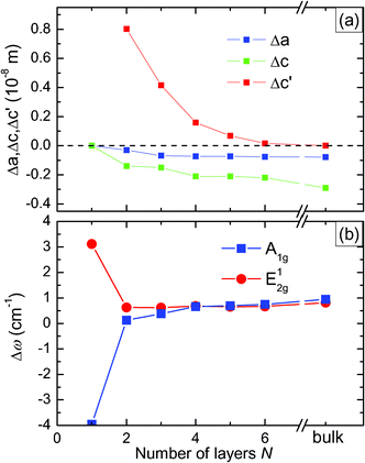 | ||
| Fig. 2 (a) Changes of the intralayer lattice parameters a and c and the interlayer distance c′ as a function of the slab thickness. (b) Frequency shifts of the A1g and E12g modes. | ||
To study the interplay between the intralayer and interlayer lattice parameters, the bond lengths in mono-layer MoS2 under biaxial strain and bi-layer MoS2 with different interlayer distances c′ are addressed in Fig. 3(a) and (b), respectively. With increasing compressive strain the S1–S2 distance increases slightly, while the S–Mo distance decreases much quicker. This leads to an increase of the frequency of the E12g mode, which corresponds to a S–Mo relative motion. When c′ grows beyond its equilibrium value, the S1–S2 distance increases quickly, suggesting that the frequency of the A1g mode decreases with the reduction of the interlayer coupling. In addition, the S1–Mo distance (S1 is located at the surface) changes only little, while the S2–Mo distance (S2 is located inside the layer) decreases rapidly with increasing interlayer coupling. Consequently, the interlayer coupling has a significant effect on the atomic positions between the two layers of bi-layer MoS2.
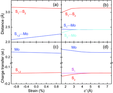 | ||
| Fig. 3 Bond distances (top) and charge transfers (bottom) for (a)/(c) mono-layer MoS2 under biaxial strain and (b)/(d) bi-layer MoS2 as a function of the interlayer distance c′. | ||
Fig. 3(c) and (d) address the atomic charges for mono-layer MoS2 under biaxial strain and bi-layer MoS2 for different interlayer distances c′, respectively. With increasing biaxial strain, the charge transfer of the S and Mo atoms changes slightly for mono-layer MoS2. With reduction of the interlayer coupling (c′ larger than the equilibrium interlayer distance), the Mo charge transfer decreases and the S2 charge transfer increases, while the S1 charge transfer is almost constant. This shows that interlayer coupling also strongly affects the electron distribution among the S and Mo atoms at the interface of the two layers, implying effects on the electronic properties.
Fig. 4 displays orbital projected electronic band structures of bulk MoS2, which have been studied experimentally and theoretically.19–21 Bulk MoS2 is an indirect band gap semiconductor with the valence band maximum (VBM) at the Γ-point and the conduction band minimum (CBM) along K–Γ. The CBM at the K-point, as well as the VBM at the Γ-point are primarily composed of the Mo  and S pz states, while the CBM along K–Γ and the VBM at the K-point are dominated by Mo
  and S px/py states. The Mo dxz/dyz states are found far off the Fermi energy.
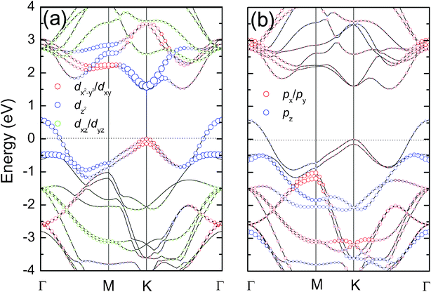 | ||
| Fig. 4 (a) Mo and (b) S orbital projected electronic band structures of bulk MoS2. | ||
Recently, few-layer MoS2 has been characterized by absorption, photoluminescence and photoconductivity experiments.6,8 It has been found that with decreasing thickness the indirect band gap shifts upwards in energy by more than 0.6 eV, which leads to a crossover to a direct band gap in the mono-layer limit. The indirect to direct band gap transition was attributed to perpendicular quantum confinement and explained by applying a zone-folding scheme for ultra thin samples. It is, however, not clear why only mono-layer MoS2 is a direct band gap semiconductor, while thicker layers of MoS2 (N ≥ 2) still exhibit an indirect band gap character.
Fig. 5(a) shows the variations of the CBM at the K-point and along K–Γ and of the VBM at the Γ and K-points with respect to the number of S–Mo–S layers. Our results are qualitatively consistent with experimental, as well as previous theoretical findings.5,6,8,21 The direct excitonic transition energy at the K-point barely changes with decreasing thickness N, whereas the indirect band gap increases by almost exactly 0.6 eV (which is the experimental value8) from the bulk to the mono-layer system. We notice that there is a sudden decrease of the VBM at the Γ-point from bi-layer to mono-layer MoS2. In the mono-layer system there is, of course, no interlayer coupling, whereas interlayer coupling still exists in few-layer MoS2. We can conclude that the absence of interlayer coupling is the origin of the direct band gap of mono-layer MoS2.
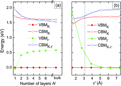 | ||
| Fig. 5 Variation of the CBM and VBM with respect to (a) the number of layers N and (b) the distance c′ between the two layers of bi-layer MoS2. CBMk refers to the K-point and CBMK–Γ to the path K–Γ, compare Fig. 4. VBMK and VBMG refer to the K-point and Γ-point, respectively. | ||
To illustrate the influence of the interlayer coupling on the electronic states of few-layer MoS2, we examine the variation of the band structure as a function of the interlayer distance c′ in bi-layer MoS2, see Fig. 5(b). Significant changes take place at the top of the valence band, where the VBM at the Γ-point drops substantially when c′ increases. For decreasing interlayer interaction the Mo  and S pz states (which mediate the interlayer coupling) shift to lower energy. The downward shift of these valence states not only results in an increase of the band gap, but also changes its nature from indirect to direct.
It is known that the interlayer interaction in graphene seriously affects the topology of the π bands, going from the mono-layer's 2D character to a 3D character for a multi-layer structure.22 The changes of the electronic structure and electron–phonon interaction are reflected by Raman fingerprints.23 Recently, mono-layer silicon (silicene) has been fabricated and a Dirac point has been observed.24,25 Silicene therefore is another prominent example of a material in which the absence of interlayer interaction induces strong changes in the electronic structure. As compared to both graphene and silicene, mono-layer MoS2 has a more complicated structure. However, the interlayer interaction plays a similarly important role for the electronic structure and vibrational properties.
In fact, MoS2 is member of a large family of structurally and chemically very closely related transition metal dichalcogenides. Its mono-layer structure results in a unique optical behaviour related to the d-electron character of its valence and conduction orbitals. In addition, few-layer MoS2 shows an anomalous behaviour of the lattice vibrations in the sense that the frequency of the E12g mode decreases and that of A1g mode increases with increasing layer thickness. It is expected that other members of the transition metal dichalcogenides with indirect band gaps, such as HfS2, MoSe2 and WS2, exhibit a similar behaviour of the lattice vibrations and electronic properties when the layer thickness decreases. Metallic transition metal dichalcogenides, such as TaS2 and NbSe2, in contrast should not behave like MoS2.
IV. Conclusion
In conclusion, we have discussed the effects of interlayer coupling on the vibrational and electronic properties of few-layer MoS2 based on ab initio calculations. When the number of S–Mo–S layers decreases, we find that the interlayer distance elongates significantly, i.e. the interlayer coupling is reduced. We have shown that the anomalous thickness dependence of the lattice vibrations in few-layer MoS2 is a consequence of these alterations of the interlayer coupling. In addition, the absence of interlayer coupling in mono-layer MoS2 explains the fact that only this system has a direct band gap, while even for bi-layer MoS2 the band gap is indirect. We note that anharmonic effects often are large for low frequencies.26 However, our line of reasoning is not affected by them as it is based on frequency shifts only. Our findings highlight that new vibrational and electronic properties, probably as exciting as those of graphene, can be expected from an ultra thin slab of vdW bounded compounds with more complex intralayer chemical structure.References
- K. S. Novoselov, A. K. Geim, S. V. Morozov, D. Jiang, Y. Zhang, S. V. Dubonos, I. V. Grigorieva and A. A. Firsov, Science, 2004, 306, 666 CrossRef CAS.
- Y. Liang, R. Feng, S. Yang, H. Ma, J. Liang and J. Chen, Adv. Mater., 2010 Search PubMed.
- X. Zong, G. Wu, H. Yan, G. Ma, J. Shi, F. Wen, L. Wang and C. Li, J. Phys. Chem. C, 2010, 114, 1963 CAS.
- X. Zong, H. Yan, G. Wu, G. Ma, F. Wen, L. Wang and C. Li, J. Am. Chem. Soc., 2008, 130, 7176 CrossRef CAS.
- H. S. S. R. Matte, A. Gomathi, A. K. Manna, D. J. Late, R. Datta, S. K. Pati and C. N. R. Rao, Angew. Chem., Int. Ed., 2010, 49, 4059 CrossRef CAS.
- A. Splendiani, L. Sun, Y. Zhang, T. Li, J. Kim, C.-Y. Chim, G. Galli and F. Wang, Nano Lett., 2010, 10, 1271 CrossRef CAS.
- C. Lee, H. Yan, L. E. Brus, T. F. Heinz, J. Hone and S. Ryu, ACS Nano, 2010, 4, 2695 CrossRef CAS.
- K. F. Mak, C. Lee, J. Hone, J. Shan and T. F. Heinz, Phys. Rev. Lett., 2010, 105, 136805 CrossRef.
- L. F. Mattheis, Phys. Rev. B, 1973, 8, 37199 CrossRef.
- P. Giannozzi, J. Phys.: Condens. Matter, 2009, 21, 395502 CrossRef.
- R. M. Martin, Electronic Structure: Basic Theory and Practical Methods, Cambridge University Press, Cambridge, 2004 Search PubMed.
- S. Baroni, S. de Gironcoli, A. Dal Corso and P. Giannozzi, Rev. Mod. Phys., 2001, 73, 515 CrossRef CAS.
- D. R. Hamann, M. Schlüter and C. Chiang, Phys. Rev. Lett., 1979, 43, 1494 CrossRef CAS.
- N. Troullier and J. L. Martins, Phys. Rev. B, 1991, 43, 1993 CrossRef CAS.
- J. P. Perdew, K. Burke and M. Ernzerhof, Phys. Rev. Lett., 1996, 77, 3865 CrossRef CAS.
- S. Grimme, J. Comput. Chem., 2006, 27, 1787 CrossRef CAS.
- P. N. Ghosh and C. R. Maiti, Phys. Rev. B, 1983, 28, 2237 CrossRef CAS.
- T. J. Wieting and J. L. Verble, Phys. Rev. B, 1971, 3, 4286 CrossRef.
- F. Mehran, R. S. Title and M. W. Shafer, Solid State Commun., 1976, 20, 369 CrossRef CAS.
- R. Coehoorn, C. Haas, J. Dijkstra, C. J. F. Flipse, R. A. de Groot and A. Wold, Phys. Rev. B, 1987, 35, 6195 CrossRef CAS.
- T. Li and G. Galli, J. Phys. Chem. C, 2007, 111, 16192 CAS.
- T. Ohta, A. Bostwick, J. L. McChesney, T. Seyller, K. Horn and E. Rotenberg, Phys. Rev. Lett., 2007, 98, 206802 CrossRef.
- A. C. Ferrari, J. C. Meyer, V. Scardaci, C. Casiraghi, M. Lazzeri, F. Mauri, S. Piscanec, D. Jiang, K. S. Novoselov, S. Roth and A. K. Geim, Phys. Rev. Lett., 2006, 97, 187401 CrossRef CAS.
- P. De Padova, C. Quaresima, C. Ottaviani, P. M. Sheverdyaeva, P. Moras, C. Carbone, D. Topwal, B. Olivieri, A. Kara, H. Oughaddou, B. Aufray and G. Le Lay, Appl. Phys. Lett., 2010, 96, 261905 CrossRef.
- B. Lalmi, H. Oughaddou, H. Enriquez, A. Kara, S. Vizzini, B. Ealet and B. Aufray, Appl. Phys. Lett., 2010, 97, 223109 CrossRef.
- S. Najmaei, Z. Liu, P. M. Ajayan and J. Lou, Appl. Phys. Lett., 2012, 100, 013106 CrossRef.
| This journal is © The Royal Society of Chemistry 2012 |