Fabrication and investigation of a new copper-doped screen-printable carbon paste's conductive mechanism by AFM†
Jun
Zhang
*a,
Zhenbing
Liang
a,
Tubshin
Hreid
a,
Wei
Guo
b and
Zhuobin
Yuan
c
aSchool of Chemistry and Chemical Engineering, Inner Mongolia University, Hohhot, 010021, P.R. China. E-mail: zhangjundoc@sina.com; Fax: +86 471 4344372; Tel: +86 471 4344372
bCollege of Environmental and Resource Sciences, Inner Mongolia University, Hohhot, 010021, P.R. China
cCollege of Chemistry and Chemical Engineering, Graduate University of the Chinese Academy of Sciences, Beijing, 100049, P.R. China
First published on 15th March 2012
Abstract
This paper presents a new low-cost water-based carbon/copper screen printing conductive paste, with commercial micron-grade graphite, nanometer acetylene black and synthesized copper submicron particles of about 226 nm in diameter as the mixed conducting fillers. The relationship between micromorphology and conductivity of the screen-printed line patterns made by the paste was monitored by atomic force microscopy. There are several different packing modes of conducting fillers relating the conductivity of screen-printed line patterns. Variations in the copper content, sintering temperature and time can remarkably affect the packing density and conductivity. The addition of copper submicron particles to the paste further improved the particle osculation by filling the interstices among the micron-grade graphite layers and arranging themselves densely with the smaller acetylene black particles. The optimized paste reached a film resistivity of 33.3 mΩ cm using screen printing and annealing at 260 °C.
1. Introduction
Conductive features such as electrodes, conductive strips and interconnects have been traditionally fabricated by the electroplating and etching processes accompanied by lithography. However, this method is time consuming, expensive and complicated. Thus, direct printing techniques such as screen printing1–4 and inkjet printing,5–6 which are simpler and less expensive, have attracted growing attention of researchers from chemistry and material science in recent years. The screen printing technology is the most promising route to fabricate conductive tracks on various substrate materials in one step. In particular, a film of constant thickness remains on the material in the screen printing method; as a result, it has been widely used to fabricate electrodes or sensors that detect antioxidants,7 glucose,8 pesticides,9 enzymes10 and DNA sequences11 for the significant advantages in flexibility, high reproducibility and high-throughput mass production.In the basic procedures of the screen printing method, the suitable conductive pastes are formed into various shapes of conductive films on the planar substrate material by employing a screen mask, followed by the appropriate thermal sintering.12 The conductive paste is an indispensable component of the screen printing method, as it greatly affects the screen printing quality and manufacturing cost. In general, the printed conductive pastes are composed of conducting fillers, polymer binders, additives, and carriers. Compared with solvent-based pastes, water-based pastes use water as the carrier in place of organic solvents. Therefore, the development and application of water-based pastes have led to a reduction in volatile organic compound emissions, and this reduction has been one of the main driving forces of product innovation.13 Moreover, the development of water-based conductive pastes that are both environmentally friendly and have a low cost is highly desirable.14
In the past few years, various conducting materials for screen-printable pastes, such as carbon,15,16 silver,17 gold,18,19 transition metals,20 doped conjugated polymers21 and metal–organic complexes,22 have been developed. Although metal-based pastes such as gold and silver exhibit high conductivity and excellent operational and thermal stabilities for the printing process, the use of these metals has been limited to a narrow range of applications due to their high cost. Doped conjugated polymer pastes have a low manufacturing cost, but their high electrical resistivity and poor electrical and thermal stabilities have discouraged their use. Conductive films based on carbon pastes have been widely used in sensing applications23–25 because of their many attractive properties. More specifically, carbon materials are more cost effective than noble metals and have relatively high electrical conductivity compared to doped conjugated polymers; in addition, they exhibit lower background currents over a wider potential window.26
In this work, we have synthesized a low-cost water-based carbon/copper screen printing conductive paste, which uses micron-grade graphite, nanometer acetylene black and submicron copper as the mixed conducting fillers. Most importantly, the effects of the packing modes of the conducting fillers on the conductive performance of the screen-printed line patterns has been revealed by atomic force microscopy (AFM).
2. Experimental section
2.1 Copper particle synthesis
Copper submicron particles were synthesized in an ambient atmosphere by the improved polyol method:5 8 g poly(N-vinylpyrrolidone) (PVP, K-30, Mw = 30![[thin space (1/6-em)]](https://www.rsc.org/images/entities/char_2009.gif) 000 g mol−1) was dissolved in 55 mL of diethylene glycol (DEG, 99%, Sigma-Aldrich). Subsequently, 0.4647 g of sodium hypophosphite monohydrate was added to the DEG solution, and the solution was heated to a reaction temperature of 140 °C in an oil bath. Using a homemade sprayer, 7.5 mL of an aqueous solution of copper(II) sulfate pentahydrate (1.3595 M) was then sparged into the hot reaction medium at a rate of 1 mL min−1. Then the suspension was rapidly cooled to 130 °C, and the solution was then slowly cooled to room temperature. The obtained particles were separated by a centrifugal separator. The particles were cleaned four times using absolute ethanol and then dried in a vacuum oven at 70 °C. The conductive paste was formulated using commercial AW875 (a vinyl resin dispersed in water, available from Dow, solid content: 39 wt%) as a binder and a carbon mixture of lamellar structured micron-grade graphite (carbon content 99%, typical particle size up to 1500 mesh, about 9 μm) and nanometer acetylene black (particle size 30–45 nm) as the conducting fillers. The ratio of the components was 20:9:1. To study the effect of additional copper, varying amounts of the as-prepared copper particles were used (0.1, 0.2, 0.3 and 0.4 g per 2 g carbon mixture).
000 g mol−1) was dissolved in 55 mL of diethylene glycol (DEG, 99%, Sigma-Aldrich). Subsequently, 0.4647 g of sodium hypophosphite monohydrate was added to the DEG solution, and the solution was heated to a reaction temperature of 140 °C in an oil bath. Using a homemade sprayer, 7.5 mL of an aqueous solution of copper(II) sulfate pentahydrate (1.3595 M) was then sparged into the hot reaction medium at a rate of 1 mL min−1. Then the suspension was rapidly cooled to 130 °C, and the solution was then slowly cooled to room temperature. The obtained particles were separated by a centrifugal separator. The particles were cleaned four times using absolute ethanol and then dried in a vacuum oven at 70 °C. The conductive paste was formulated using commercial AW875 (a vinyl resin dispersed in water, available from Dow, solid content: 39 wt%) as a binder and a carbon mixture of lamellar structured micron-grade graphite (carbon content 99%, typical particle size up to 1500 mesh, about 9 μm) and nanometer acetylene black (particle size 30–45 nm) as the conducting fillers. The ratio of the components was 20:9:1. To study the effect of additional copper, varying amounts of the as-prepared copper particles were used (0.1, 0.2, 0.3 and 0.4 g per 2 g carbon mixture).
2.2 Preparation of the conductive paste
The conducting particles were dispersed in a mixed solvent of deionized water and diethylene glycol monobutyl ether. The solid loads of all the pastes were about 47 wt%. The water loads of all the liquid solvents were more than 72.4 wt%. The formulated pastes were blended for one hour using a high-speed mixer, followed by two hours of static defoaming.2.3 Printing
Single-pass straight lines (1.860 cm × 0.230 cm × 0.012 mm) were printed on glass slides by the screen printing process and were then dried overnight at room temperature before being placed in a temperature-controlled oven. A range of different temperatures were used in this study: 120, 150, 180, 220, 260 and 300 °C. Each printed track was cured for 90 min in order to saturate the film resistivity to a certain value.2.4 Characterization
The micromorphology of the copper particles and the pattern of the printed film after drying were investigated by AFM (SP-II, Beijing Zhongke Mechanical & Electrical Equipment Co., China). The hydrodynamic diameters of the copper particles and the particle size distribution data were measured using a Malvern Particle Sizer (Nano-S, Malvern Instruments, England). The conductivity measurements were performed using the linear sweep voltammetry method. Briefly, two commercial clamps that maintained the same pressure for each printed sample were attached to the ends of a single carbon conductive line with a length of 1.80 cm. The wires were guided from the clamps to the counter electrode and the working electrode of the LK98B II Electrochemical Analyzer (Lanlike Co. Ltd, Tianjin, China), which was connected to a computer that recorded the resistance.3. Results and discussion
3.1 Characteristics of copper submicron particles
Fig. 1a depicts the size distribution based on the Malvern Particle Sizer data; most of the particles fall between 150 and 350 nm in diameter with a number-weighted mean of 226 nm, and the percentage of metallic copper under 100 nm and beyond 350 nm in diameter is less than 1%. The AFM image (Fig. 1b) of the typical polyol-derived copper submicron particles show these prepared copper submicron particles were narrowly dispersed spherical particles without agglomeration or aggregation. The fabricated copper particles appear fresh red. It is real metallic copper, not partly oxidized or oxides which appear wine red or black. The further conductivity experiment has also proved this, in which impacted bare copper particles separated from PVP by chloroform have a conductivity similar to that of pure copper. | ||
| Fig. 1 Particle size distribution histogram of synthesized metallic copper particles in ethanol solution (a) and a contact-mode AFM image of the copper particles on a mica flake (b). | ||
3.2 Effect of electrical resistivity by different contact models
Fig. 2a shows the tracks printed by the screen printing process. The AFM images in Fig. 2c–2f show the surface micromorphology of the printed tracks sintered at 120 °C for 90 min. It should be noted that there are three contact models of the conductive material in the micron-grade graphite and nanometer acetylene black-filled film: (I) the tight combination of the lamellar structured micron-grade graphite layers (Fig. 2c, 2d and 2f), (II) the contact of the graphite layers by a monolayer or few-layers of acetylene black (Fig. 2c) and (III) the contact of the graphite layers by the multilayers of acetylene black (Fig. 2e). Each of these models can affect the electrical resistivity of the printed tracks in the structure. | ||
| Fig. 2 The tracks (1.860 cm × 0.230 cm × 0.012 mm) printed by the screen printing process (a) and the variation in resistivity of the carbon-filled film and the different carbon–copper mixed films as a function of the annealing temperature (b). The contact-mode AFM images of the surface micromorphology of the films prepared from (c, e) carbon-filled and (d, f) carbon–copper mixed conductive paste (0.2 g copper per 2 g carbon mixture) and sintered at 120 °C. The insets (I–V) show the interfacial structure models of the micron-grade graphite layers (gray lamellas), nanometer acetylene black (small dark particles) and submicron copper (spherical particles). | ||
The electrical resistivity of the printed tracks after different temperature treatments is shown in Fig. 2b. As expected, when the copper submicron particles were added, the film conductivity of the printed tracks increased for curing temperatures (CT) of 150, 180 and 220 °C. This increase was not only due to the higher conductivity of the metallic copper, but also mainly because the copper submicron particles filled some interstices between the micron-grade graphite layers that the nanometer acetylene black particles were not large enough to occupy. However, the film conductivity of the printed tracks cured at 120 °C decreased when the copper submicron particles were added. From the AFM images, it can be seen that there are other kinds of packing models when the spherical submicron copper particles are mixed with the lamellar structured micron-grade graphite and nanometer acetylene black. The AFM images of Fig. 2d and 2f show two different kinds of packing were obtained when the copper particles are added. In Fig. 2d (IV), similar to the binary conductivity mixture, the monolayer spherical copper particles with different sizes enlarge the interstices between the micron-grade graphite layers, which were originally filled by nanometer acetylene black. On the other hand, in Fig. 2f (V), the spherical copper particles are densely arranged and fixed in contact with each other, similar to a grape interlink structure, between the different layers of the lamellar structured micron-grade graphite. In addition, the nanometer acetylene black or spherical particles of small sizes fill the interstices among the large-size particles to produce a ternary conductivity mixture.
These two kinds of filling mode indicate that the addition of metallic copper submicron particles may actually have two opposing effects: the conductivity may decrease due to the enlarged interstices between the graphite layers (model IV), and the conductivity may increase due to the improved packing density (model V). The enlarged interstices between the graphite layers (Fig. 2d) and the interstices formed by the material shrinking after curing at 120 °C (shown by arrow in Fig. 2f) cause the conductivity to decrease overall. The enhancement in the packing density indicates that there are more inter-particle contact areas, which enables the films to develop a denser structure when annealed at a higher temperature, thus resulting in improved conductivity.
These packing modes of conducting fillers exist in the actual screen-printed tracks, in which the conductivity depends on the connection status and density of the conductive filler. The higher curing temperature markedly enhances the connection of conductive filler, and thus greatly reduces the resistivity. The copper particles altering the filler packing density, can also affect the resistivity (Fig. 2b).
3.3 Effects of film micromorphology and electrical resistivity by different thermal treatment temperatures
The AFM images in ESI Fig. S1† show the surface micromorphology of the printed tracks sintered at different temperatures for 90 min each. There is an obvious sintering effect with the heat treatment. At 120 °C, each particle appears unchanged and can be clearly observed (a, b). However, after heating at 180 °C for 90 min, the sintering effect is obvious, as the boundaries between most particles were blurry (c). At around 260 °C, most of the boundaries between particles disappeared due to sintering (d), and consequently, the electrical resistivity decreased to the lowest values. The corresponding data for electrical resistivity are shown in Fig. 2b.At heat treatment temperatures below 130 °C, for example at 120 °C, the resistivity of the carbon–copper mixed conductive paste was significantly greater than that of the carbon-filled paste. Presumably, in addition to the enlarged interstices between the graphite layers (Fig. 2d and 2f) at this stage, the copper particles were likely still covered with a layer of the protective agent (PVP molecules) and could be considered to be an insulated material. Consequently, some of the graphite layers and acetylene black particles insulated by these non-conducting copper particles were barely in contact with each other, resulting in the increasing resistivity, as shown in Fig. 2d (IV) and 2f (V). When the heating temperature reached the melting point of PVP (Tm = 130 °C), the PVP molecules would melt and move away from the particle surface to coalescence together and separate from the particles; as a result, the copper particles would then touch each other or the graphite layers and acetylene black particles and thus conduct electricity. Further heating would enlarge the contact area among the particles and continue the densification process of sintering, thus lowering the resistivity. As compared to the carbon-filled conductive paste, the decrease in the resistance of the carbon–copper mixed conductive paste was relatively fast as the temperature increases above 130 °C. At around 220 °C, the descent of resistance was at a minimum, and the paste gradually reached the CT.
From Fig. 2b, the CT of the carbon–copper mixed conductive paste was about 220 °C, whereas the CT of the carbon-filled conductive paste was about 260 °C. This difference indicates that the addition of metallic copper submicron particles can facilitate faster densification compared to when only graphite and acetylene black are present in the film. At around 300 °C, some graphite and acetylene black begin to burn off, and the resistance of the paste rebounds.
Fig. 3 shows the resistivity variation of the carbon-filled film and the carbon–copper mixed film with curing time. Firstly, the resistivity of the films decrease fast with increasing curing time. Then, the resistivity begins to increase for the carbon-filled film or decrease slowly for the carbon–copper mixed film after 90 min. This indicates that the carbon also causes some loss with a longer curing time when being sintered at 260 °C, and 90 min is enough to saturate the film resistivity to a certain value.
 | ||
| Fig. 3 The resistivity of the carbon-filled film and the carbon–copper mixed film (0.2 g copper per 2 g carbon mixture) as a function of curing time, sintered at 260 °C. | ||
3.4 Effect of the submicron copper content on screen printing of the conductive carbon paste
Fig. 4a–4d show the packing detail of spherical particles on the flat surface of micron-grade graphite. This figure reveals that the carbon–copper mixed film has a much denser micro-structure compared to the carbon-filled film when they are annealed at the same temperature. From the image in Fig. 4d, it should also be observed that increasing the copper content does not further facilitate the packing density of the film. A relatively low concentration, for example 0.1 g copper, was sufficient to result in a conductive network throughout the whole film.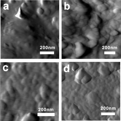 | ||
| Fig. 4 The contact-mode AFM images of the screen printed conductive carbon paste films sintered at 180 °C for 90 min with the following copper contents: 0 (a), 0.1 (b), 0.2 (c) and 0.4 g (d). | ||
To discuss the effect of the density improvement, the film resistivity was measured as a function of the copper content of the conductive pigments, as shown in Fig. 2b. The film conductivity for all samples increased with increasing CT until 260 °C (33.3 mΩ cm with copper content of 0.2 g). After annealing at 180 °C, the film composition with a copper content of 0.1 g exhibited the lowest electrical resistivity (249 mΩ cm) compared to the 0 g copper content (403 mΩ cm), 0.2 g copper content (273 mΩ cm), 0.3 g copper content (373 mΩ cm) and 0.4 g copper content (431 mΩ cm). It was expected that the film composition with a copper content of 0.4 g would exhibit a higher conductivity than the other films because of its higher copper content. On the contrary, the film with the copper content of 0.1 g copper, which was a relatively low concentration, produced the best conductive track at 180 °C. This result may be due to the higher content of insulating PVP in the higher copper content film. We believe that the amount of PVP is the predominant factor in determining the conductivity because the incorporation of increasing amounts of copper does not further improve the packing density of the film. This belief is supported by the atomic force micrograph studies of Fig. 4b–4d.
4. Conclusions
The reported carbon–copper mixed water-based conductive paste seems to offer an economically attractive route to develop an environmentally friendly paste with good conductivity at low sintering temperatures. It could form continuous smooth conductive tracks on a glass substrate using the screen printing process, and its resistivity reached 33.3 mΩ cm when annealed at 260 °C. Based on the AFM micromorphology images, five types of packing models of the conducting fillers were monitored. The copper particles further improve the particle packing density by filling the interstices among the micron-grade graphite layers and arranging themselves densely with the smaller acetylene black particles, which improves the conductivity at lower sintering temperatures. The relationship between micromorphology and conductivity of screen-printed line patterns could aid in preparing higher-performance low-cost carbon–metal screen-printable conductive pastes.Acknowledgements
This work was partially supported by the National Natural Science Foundation of China (40861018, 20965004 and 21165011), the “Chunhui Program” of the Ministry of Education (Z2007-1-01039) and the Natural Science Foundation of the Inner Mongolia Autonomous Region (200607010210, 20080404MS0611 and 2011BS0202).References
- T. S. Mann and S. R. Mikkelsen, Anal. Chem., 2008, 80, 843 CrossRef CAS.
- W. Dungchai, O. Chailapakul and C. S. Henry, Anal. Chem., 2009, 81, 5821 CrossRef CAS.
- G. Aragay, A. Puig-Font, M. Cadevall and A. Merkoçi, J. Phys. Chem. C, 2010, 114, 9049 CAS.
- Z. J. Zou, Y. Liu, H. Y. Li, Y. C. Liao and C. S. Xie, J. Comb. Chem., 2010, 12, 363 CrossRef CAS.
- B. K. Park, D. Kim, S. Jeong, J. Moon and J. S. Kim, Thin Solid Films, 2007, 515, 7706 CrossRef CAS.
- K. Woo, D. Kim, J. S. Kim, S. Lim and J. Moon, Langmuir, 2009, 25, 429 CrossRef CAS.
- J. F. Liu, B. Su, G. Lagger, P. Tacchini and H. H. Girault, Anal. Chem., 2006, 78, 6879 CrossRef CAS.
- L. X. Cheng, S. Y. Deng, J. P. Lei and H. X. Ju, Analyst, 2012, 137, 140 RSC.
- X. Llopis, N. Ibáñez-García, S. Alegret and J. Alonso, Anal. Chem., 2007, 79, 3662 CrossRef CAS.
- D. Hernández-Santos, M. Díaz-González, M. B. González-García and A. Costa-García, Anal. Chem., 2004, 76, 6887 CrossRef.
- C. A. Marquette, M. F. Lawrence and L. J. Blum, Anal. Chem., 2006, 78, 959 CrossRef CAS.
- J. P. Metters, R. O. Kadara and C. E. Banks, Analyst, 2011, 136, 1067 RSC.
- A. Meteš, D. Kovačević, D. Vujević and S. Papić, Water Res., 2004, 38, 3373 CrossRef.
- F. J. Rawson, W. M. Purcell, J. Xu, R. M. Pemberton, P. R. Fielden, N. Biddle and J. P. Hart, Talanta, 2009, 77, 1149 CrossRef CAS.
- X. J. Ma and H. L. Xia, J. Hazard. Mater., 2009, 162, 386 CrossRef CAS.
- C. Cougnon, Electrochim. Acta, 2006, 51, 4142 CrossRef CAS.
- W. Yin, D. H. Lee, J. Choi, C. Park and S. M. Cho, Korean J. Chem. Eng., 2008, 25, 1358 CrossRef CAS.
- S. Susmel, G. G. Guilbault and C. K. O'Sullivan, Biosens. Bioelectron., 2003, 18, 881 CrossRef CAS.
- E. S. Fakunle, Z. P. Aguilar, J. L. Shultz, A. D. Toland and I. Fritsch, Langmuir, 2006, 22, 10844 CrossRef CAS.
- A. Müller, T. Brinz and U. Simon, J. Comb. Chem., 2009, 11, 138 CrossRef.
- X. Y. Hao, G. S. Gai, Y. F. Yang, Y. H. Zhang and C. W. Nan, Mater. Chem. Phys., 2008, 109, 15 CrossRef CAS.
- C. W. Sele, T. von Werne, R. H. Friend and H. Sirringhaus, Adv. Mater., 2005, 17, 997 CrossRef CAS.
- M. Dequaire and A. Heller, Anal. Chem., 2002, 74, 4370 CrossRef CAS.
- J. P. Hart, A. Crew, E. Crouch, K. C. Honeychurch and R. M. Pemberton, Anal. Lett., 2004, 37, 789 CrossRef CAS.
- G. Fouad, S. Ledru, N. Ruille, F. Lantier and M. Boujtita, Anal. Chim. Acta, 2006, 570, 158 CrossRef.
- F. Lucarelli, G. Marrazza and M. Mascini, Langmuir, 2006, 22, 4305 CrossRef CAS.
Footnote |
| † Electronic Supplementary Information (ESI) available. See DOI: 10.1039/c2ra20102j/ |
| This journal is © The Royal Society of Chemistry 2012 |