Controlled synthesis of CdE (E = S, Se and Te) nanowires†
Lifei
Xi
a,
Kheng
Hwee Chua
a,
Yanyuan
Zhao
c,
Jun
Zhang
c,
Qihua
Xiong
cd and
Yeng
Ming Lam
*ab
aSchool of Materials Science and Engineering, Nanyang Technological University, 50 Nanyang Avenue, Singapore 639798
bInstitut für Werkstoffe der Elektrotechnik II, RWTH Aachen, Sommerfeldstraße 24, D-52074, Aachen, Germany. E-mail: ymlam@ntu.edu.sg (Y.M. Lam); Fax: +65 6790 9081
cDivision of Physics and Applied Physics, School of Physical and Mathematical Sciences, Nanyang Technological University, 21 Nanyang Link, Singapore 637371
dDivision of Microelectronics, School of Electrical and Electronic Engineering, Nanyang Technological University, Singapore 639798
First published on 27th March 2012
Abstract
This work focused on a catalyst-free solution-based method to synthesize single-crystal CdE (E = S, Se and Te) nanowires. Using the hot coordinating solvents method, we have successfully synthesized high aspect ratio CdE nanowires. In this paper, we present our very recent results on the synthesis of CdTe nanowires and summarize our understanding of the effect of reaction parameters on the growth of CdE nanowires. The reaction parameters include ligands for Cd-complexes and E-complexes, ligand-to-Cd mole ratio, Cd-to-E mole ratio, precursor concentration, reaction temperature and the injection process. We propose the optimum conditions for the growth of CdE nanocrystals with a large aspect ratio. Possible growth mechanisms were also investigated using time-dependent studies. Furthermore, a Raman study shows a higher concentration of tellurium on the surface of CdTe nanowires. This is understandable because the free energy of Te is smaller than that of CdTe and thus Te crystals can easily form during the synthesis. Our high aspect-ratio nanowires have good dispersibility and exhibit huge potential applications in areas such as solution processed photovoltaic cells and transistors.
Introduction
In recent years, semiconductor nanowires have attracted considerable attention due to their potential applications in biosensors,1 logic circuits,2 nonvolatile memories,3 field-effect transistors (FETs) 4 and photovoltaics.5,6 These applications require semiconductor nanowires with well-controlled chemical composition and uniformity in dimensions and morphology.7,8 Various techniques, including chemical vapor deposition (CVD),9 vapor-liquid-solid (VLS),10 solution-liquid-solid (SLS),11,12 template directed electrodeposition,13 self-assembly via an oriented attachment,14,15 surfactant-assisted aqueous phase synthesis methods16 have been reported to be successful in synthesizing nanowires. Among all these methods, VLS and SLS are the most commonly used techniques to synthesize nanowires with high crystallinity and high aspect ratios. However, these methods require a catalyst activation step at the beginning of growth, which may change the chemical uniformity of the nanowires and thus affect their potential applications.17 Self-assembly via an oriented attachment is another promising method to synthesize nanowires in solution. It is carried out using dot-shaped nanocrystal self-assembly via an oriented attachment process. The driving force for this process is either the presence of a dipole moment in the nanocrystals or the reduction of surface tension through the elimination of surfaces via attachments.14,18 The advantages of this method are it is catalyst-free and requires lower temperatures than the SLS method. Several materials, including ZnO19 and ZnSe20 nanorods, CdSe14,18 CdTe14 and PbSe21 nanowires, have been obtained through this process. However, this method requires two necessary steps: synthesis of small uniform nanocrystals and following that a long reaction time (7 days) for pearl-necklace aggregation and subsequent fusion of the fragments into nanowires.18 Another technique, the surfactant-assisted aqueous phase synthesis method, has other advantages, such as a comparatively low reaction temperature and it is a simple process. But the size distribution and crystallinity of the nanocrystals are not that good due to decreased control during the nucleation and growth stages. Bao et al. recently reported their synthesis of thiol-capped CdTe nanowires in aqueous phase.16 Although the CdTe nanowires have large aspect ratio, they have poor crystallinity.Alternatively, the hot coordinating or non-coordinating solvents method is also a catalyst-free and solution-based synthesis method.22,23 This method is more desirable due to several advantages, including the process being simple, a relatively low reaction temperature (< 330 °C), and the nanocrystals synthesized have well-controllable shape and size uniformity.24 It has been successfully used to synthesize high-quality CdE (E = S, Se and Te) nanodots, nanorods and tetrapods.22-24 However, CdE nanowires with a high aspect ratio are still rarely reported to be synthesized using this method.25 In our previous studies,26,27 we have reported the successful synthesis of CdS and CdSe nanowires. Monodisperse CdS nanowires were around 600 nm in length and 3.5 nm in diameter. We studied the effects of the reactant ratio, the precursor ratio, the precursor concentration, the precursor injection process and the type of ligand on the surface and morphology of the nanowires. A good balance between nucleation and growth favors formation of high aspect ratio nanocrystals. Later, after a systematic investigation of several reaction parameters, including ligands for Cd complexes and precursor concentration, CdSe nanowires with a length of around 220 nm and a diameter of 8 nm were successfully synthesized.27 In that study, we manipulated the cleavage rate of P = Se and Cd complexes via a change in the type of ligands used to form the complexes and doubled the precursor concentration to achieve a good balance between nucleation and growth. Very recently, based on our understanding of the growth mechanism, we successfully synthesized CdTe nanowires with a length of around 210 nm and a diameter of 7.5 nm after a systematic investigation of the reaction parameters. We found that single continuous injection is very important for the formation of high aspect ratio nanocrystals, although this method was found to be not so important for the growth of CdSe nanowires. This difference is due to the faster cleavage rate of trioctylphosphine = Te (TOP = Te) than TOP = Se. With multiple injections, fast cleavage of TOP = Te results in more nuclei and hence more rapid depletion of the monomers. Thus, the precursor concentration available for the rods to grow into nanowires is reduced substantially. However, a single continuous injection will maintain a relatively high monomer concentration in the solution which is thought to be a prerequisite for anisotropic growth.23,28
CdE (bulk: Eg = 2.4 eV for CdS, Eg = 1.73 eV for CdSe and Eg = 1.45 eV for CdTe at 300 K), has a high optical absorption coefficient and represents one of the most important group II–VI semiconductors.29,30 These materials have been widely used in electronic and optical devices. Currently, CdE nanorods or wires have become important potential building blocks for new electronic and optical nanodevices such as lasers,31 transistors,32 light-emitting diodes33,34 and photovoltaic35,36 devices. As the electronic and optical properties of nanocrystals are dependent on the dimensions of these crystals, the issue of how to control the growth of CdE nanowires is one of the most challenging issues in chemistry and materials science. In this paper, we will report on the controlled synthesis of high-quality CdE nanowires using the hot coordinating solvents method. On top of reporting our recent results on the synthesis of CdTe nanowires, we will summarize our understanding of the effects of reaction parameters on the growth of CdE nanowires.
Experimental
Materials
TOPO (trioctylphosphine oxide, 99%) and tellurium powder (Te, 99.8%) were purchased from Sigma-Aldrich. TOP (trioctylphosphine, 90%), TBP (tributylphosphine, 90%) and cadmium oxide (CdO, 99.95%) were purchased from Fluka. TPP (Triphenylphosphine, 95%) was purchased from Tokyo Kasei Kogyo Co. Ltd. HPA (hexylphosphonic acid, 100%), DDPA (dodecylphosphonic acid, 100%), TDPA (tetradecylphosphonic acid, 100%) and ODPA (octadecylphosphonic acid, 100%) were purchased from Polycarbon Inc.Synthesis of CdS and CdSe nanocrystals
The details of the synthesis of CdS and CdSe nanocrystals can be found in ref. 26 and 27Synthesis of CdTe nanocrystals
The synthesis procedure was similar to that of CdS and CdSe nanocrystals. In a typical synthesis, 0.128 g of CdO, 0.500 g DDPA (0.668 g of ODPA, 0.557 g of TDPA or 0.232 g of HPA) and 2.5 g TOPO were added to a 25 ml three-neck flask equipped with a condenser and a thermocouple adapter. The mixture was degassed at room temperature for 10 min. The flask was then refilled with N2 and the temperature was gradually raised to 300 °C to dissolve the CdO. After the CdO was dissolved and Cd-complexes formed, the solution turns colorless. In another 25 ml three-necked flask, 0.128 g of Te and 3.5 g of TOP was prepared. The Te mixture was heated up to 200 °C under N2 flow to form a clear yellow solution indicating that Te-complexes have been formed. After that, the solution was allowed to cool down to room temperature. When the Cd-complex reaction mixture was stabilized at about 300 °C, the Te-complex reaction mixture was continuously injected with different durations. After the injection, the temperature was maintained at 300 °C for subsequent growth. The reaction was stopped by removing the flask from the heating mantle. The nanowires were then washed twice with toluene/ethanol and redissolved in toluene for further characterization.Characterization
TEM was carried out using a JEOL 2010 microscope fitted with a LaB6 filament and the acceleration voltage used was 200 kV. Ultraviolet-visible (UV-Vis) absorption spectra of the nanocrystals were obtained using a Perkin Elmer Lambda 900 UV/Vis/NIR spectrophotometer. Thin film X-ray diffraction (XRD) studies were carried out on a Shimadzu XRD 6000 using Cu-Kα radiation at 40 kV and 40 mA. Raman scattering spectroscopy was conducted at room temperature using a Micro-Raman spectrometer (Horiba-JY T64000) in a backscattering configuration. A solid state laser (λ = 532 nm) laser was used to excite the sample. The back-scattered signal was collected through a 100× objective and dispersed by a 1800 g mm−1 grating under triple subtractive mode. The spectral resolution was 1 cm−1 and the lowest available frequency was 5 cm−1. The laser spot at the sample surface was around 1 μm and the power could be measured by a power meter through a 10× objective.Results and discussion
Influence of different ligands on the Cd complexes
In our studies, we found that phosphonic acids play many important roles in the reaction. These phosphonic acids are responsible for dissolving CdO powder,37,38 cleavage of the Cd = P double bond during the cleaving stage,39 controlling monomer solubility as well as selective adhesion to particular facets on the nanocrystals during the nucleation/growth stages.40 Thus, phosphonic acids with different alkyl chain lengths give rise to different cleavage rates which will affect the nucleation and growth. In the synthesis of CdS nanowires, we found that the phosphonic acids with longer alkyl chains, such as ODPA and TDPA, were better at controlling the morphology of CdS nanocrystals than those with shorter alkyl chains, such as DDPA and HPA. The latter can only generate nanoneedles with a rough surface or nanocrystals with poor control of morphologies. A mixture of short rods, branches, and nanowires can be found. We proposed that the reason for the poor control over the morphology offered by phosphonic acids with shorter alkyl chains is due to the higher reactivity of the Cd-ligand complexes. The reactivity of Cd-ligand complexes affects the P = S cleavage kinetics and the nucleation/growth rate of anisotropic nanocrystals.39 Furthermore, complexes with lower reactivity allow the monomers to adjust their position on the surface of the nanocrystal before the binding occurs.41 Therefore, Cd-ODPA complexes which provide both a low diffusion rate and low reactivity are good candidates for generating nearly monodisperse and high aspect ratio CdS nanowires. CdS nanowires with a monodisperse diameter of 3.5 nm and a length of about 600 nm were successfully synthesized in that study (see Fig. 1a).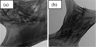 | ||
| Fig. 1 TEM images of (a) CdS and (b) CdSe nanowires synthesized for this study. | ||
During the synthesis of CdSe and CdTe nanowires we found that DDPA and TDPA with medium alkyl chain lengths are better at controlling the morphology of CdSe and CdTe nanocrystals than shorter alkyl chain phosphonic acid (HPA) and longer alkyl chain phosphonic acid (ODPA). CdSe nanowires with a length of 220 nm and a diameter of 8 nm were successfully synthesized using DDPA (see Fig. 1b). We propose that on top of the medium diffusion rate and reactivity provided by DDPA and TDPA, the fast cleavage rate of P = Se and Te bonds compared to P = S bonds affects the balance between nucleation and growth. DDPA or TDPA as ligands for Cd-complexes are well matched with TOP as the ligand for Se or Te complexes. A good balance in the reaction conditions are achieved when these ligands are used and thus anisotropic growth is favored.
TEM images of CdTe nanocrystals synthesized with different ligands on Cd complexes are shown in Fig. 2. It can be seen that HPA produces spherical nanocrystals with a diameter of 30 nm (see Fig. 2a). As the length of the alkyl chain of phosphonic acids is increased (DDPA and TDPA), the length of the nanocrystals increased substantially (see Fig. 2b–c). Using DDPA, single-crystal CdTe nanowires with a length of 210 nm and a diameter of 7.5 nm were produced. The growth of CdTe nanowires is along the preferred [001] direction and can be indexed using hexagonal CdTe (JCPDS card No. 19-0193) (see Fig. S1 and S2 for XRD patterns and HRTEM images†). The length of the nanowires synthesized with TDPA was 130 nm and the diameter was constant. Further increasing the length of the alkyl chain of phosphonic acid (ODPA), we obtained CdTe nanorods with a length of 31 nm and a diameter of 6.7 nm (see Fig. 2d). A possible reason for the high aspect ratio nanowires formed when using DDPA as compared to TDPA and ODPA is due to the optimal balance between nucleation and growth. In the following, we will present studies of the effect of the different E ligands on nanocrystal morphology when ODPA was used for CdS and DDPA was used for CdSe and CdTe.
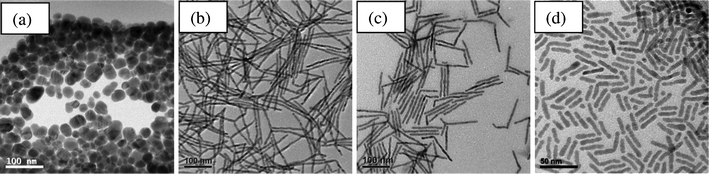 | ||
| Fig. 2 TEM images of CdTe nanocrystals synthesized with different ligands for Cd complexes at 300 °C: (a) HPA, (b) DDPA, (c) TDPA and (d) ODPA. The ligand used for the Te complexes is TOP. | ||
Influence of the different ligands on E complexes
Compared with Cd-complexes, the different ligands for E-complexes were also found to have a strong effect on the morphology. After mixing TOP with E powder, the TOP = E bond was formed. The formation of the TOP = E double bond and the cleavage of it can be observed by FT-IR. FT-IR spectra of pure TOP, TOP-S complexes, CdS nanocrystals after injections at 10, 60 and 95 min in the frequency range 400–2000 cm−1 are shown in Fig. 3. It can be seen that the difference between the spectra from pure TOP and TOP = S complexes is the presence of vibration at around 598 cm−1. The presence of a strong band at 598 cm−1 in the spectrum of TOP = S complexes is due to the presence of R3P = S.42 This confirms that TOP and S formed a double bond after stirring for 30 min at room temperature. The peak shift of the maximum from 598 cm−1 for TOP = S complexes to 575 cm−1 in the CdS nanocrystals may indicate that the cleavage has to occur prior to CdS formation. On top of this, the peak intensity for this region also decreased with time when compared to spectra after injections at 10, 60 and 95 min. These results also suggest that the cleavage of the P = S bond happened. Liu et al. also found this to be the case using NMR to study the precursor evolution in II–VI nanocrystals synthesis.39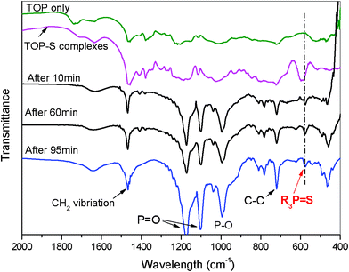 | ||
| Fig. 3 FT-IR spectra of pure TOP, TOP = S complexes, CdS nanocrystals after final injection 10, 60 and 95 min. | ||
It is worth mentioning that the conditions to form colorless TOP = S, TOP = Se and yellow transparent TOP = Te complexes are different. The formation of TOP = S complexes, takes 30 min of stirring at room temperature. At least 1 h of stirring at room temperature was needed to form TOP = Se complexes. However, for the formation of TOP = Te complexes, heating up to 200 °C and stirring for at least 1.5 h was required to form a yellow transparent solution. The difference in the formation of the TOP = E double bond was related to the cleavage rate of P = E in the subsequent reaction.
In the synthesis, a common phenomena is that the time taken for the color of the solution with TBP = E to change is slower compared to that taken by the solution containing TOP = E. For example, the time taken for the color of the solution with TBP = S to change is slower by 20 min compared to that taken by the solution containing TOP = S. The color of the solution containing TBP = S remained colorless for 30 min after all injections, changed to gray after 40 min, then to light yellow after 50 min and deep yellow after 95 min (see Fig. 4a). For the solution containing TOP = S, all these color changes take place within 30 min after all injections. Furthermore, when TBP is used, the maximum aspect ratio is reached after 4 h while it takes 2 h for the nanocrystals synthesized in the TOP complexed solution to reach its maximum aspect ratio. TBP tends to slow down the reaction as compared to TOP. This was a common phenomenon in our studies. For example, we found that the time taken for the color of the solution with TBP = Se to change is slower by several minutes compared to that taken by the solution containing TOP = Se. We think that the difference in the reaction rates cannot be explained by the steric effect because the octyl group offers an even larger steric hindrance to the cleavage of the P = E bond compared to the butyl group. It is very likely that TBP = E has a stronger binding energy than TOP = E because the octyl group is less stabilizing to the P = E bond than the butyl group.
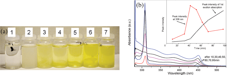 | ||
| Fig. 4 (a) Solution color change vs. time (after the 4th injection of a multiple injection process 10, 30, 40, 50, 60, 70 and 95 min) during the synthesis of CdS nanocrystals. (b) UV-Visible absorption spectra of CdS nanocrystals. An absorption intensity change at 308 nm and the 1st exciton absorption around 440 nm can be seen. Inset shows the change in intensity of the peaks at 308 and 440 nm as a function of time of injection. | ||
When using TPP, we found that the color change for the TPP complexed solution is significantly shorter than that for TOP and TBP complexed solutions. During the cleavage of the P = E, TPP with three benzene rings will prevent alkylphosphonate attacking the (TPP = E)-Cd complex. We propose that this difference is indeed due to the steric effect which results in a lower cleavage rate and hence a lower CdE monomer concentration at the initial stage.27 In addition, these three benzene rings can further prevent the CdE monomer binding onto the nanocrystal surface. Thus, it is proposed that an ideal E complex ligand will be TOP for the synthesis of high aspect ratio CdE nanocrystals. The time-dependent optical properties of CdS nanocrystals are shown in Fig. 4b. It can be seen that there are three obvious peaks in the absorption spectra. The first peak is centered at 308 nm is an indication of the presence of CdE monomers. Similar characteristic peaks were observed in the synthesis of CdSe and CdTe nanocrystals. The peaks for CdSe and CdTe are centered at 349 and 376 nm, respectively. The second obvious peak is located at around 440 nm, which is related to the diameter of the nanorods or wires. As the reaction progresses, the 440 nm peak intensity gradually increases and the peak center is red shifted. The change in these two peak intensities is shown in the inset in Fig. 4b. Between 10 min and 40 min after all injections the peak intensity reaches its maximum. This shows that the nucleation rate is quite fast. The increase in intensity and the decrease in width of both the 1st and 2nd exciton absorption peaks is an indication of the increase in monodispersity of the diameter of the nanocrystals as the growth progresses.37,43,44
Influence of the ligand-to-Cd mole ratio
As discussed, ligands are involved in the formation of complexes, cleavage, nucleation and growth.37–40 Thus, the ligand-to-Cd mole ratio is an important factor for the synthesis of high-quality CdE nanowires. It was reported that 2 mol of phosphonic acid is required to dissolve 1 mole of brown CdO powder so that all the cadmium ions formed complexes with the phosphonic acids.37–39 When the phosphonic acid-to-Cd mole ratio is less than 2, CdO cannot be completely decomposed to form a colorless Cd complex solution at the reaction temperature. This is consistent with our results using HPA, DDPA, TDPA and ODPA. We found that although the phosphonic acid-to-Cd mole ratio is slightly lower than 2, the XRD pattern of the final CdE products did not show any CdO peaks. A possible reason is that as the reaction progressed, previously formed anhydrides of phosphonic acid may undergo subsequent hydrolysis and regenerate phosphonic acids.39 These regenerated phosphonic acids can further dissolve unreacted CdO in the solution. A lower monomer concentration at the initial stage decreases the growth rate of the CdE nanocrystals and the presence of undissolved CdO particles can also disturb the nucleation/growth. Thus the morphology of nanocrystals with a lower phosphonic acid-to-Cd mole ratio is a mixture of dots and rods in the synthesis of CdS nanocrystals. Previously, Liu et al. studied the precursor evolution in group II–VI nanocrystal synthesis and proposed possible reaction pathways.39 Here, modified reaction pathways and chemicals used for this reaction are proposed as shown in Fig. 5. According to the reaction proposal, the whole reaction process can be explained with these stages: with the injection of the TOP = E complexes, (TOP = E)-Cd-phosphonic acid complexes form at the reaction temperature. Subsequently, a nucleophilic attack of alkylphosphonate on the (TOP = E)-Cd-phosphonic acid complexes results in the cleavage of the phosphorus chalcogenide double bond (TOP = E).39 This process generates initial CdE monomers, TOPO and phosphonic acid anhydrides. CdE monomers form magic sized nanoclusters (called a nucleation step) after achieving a supersaturation of monomers and grow larger by incorporating additional monomers still present in the solution with the binding effect of phosphonic acid. Thus ligands for Cd complexes and E complexes are important in the conversion of precursor molecules to CdE nanocrystals because they first act as reagents. In the later stage, regenerated ligand from Cd complexes becomes a binding agent, which affects anisotropic growth.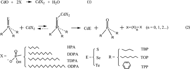 | ||
| Fig. 5 Reaction pathways to dissolve brown CdO powder (1) and produce CdE monomers (2) in the reaction. | ||
When the phosphonic acid-to-Cd mole ratio was equal to 2, high aspect ratio CdE nanowires can be obtained (see Fig. 1a–b and 2b). Further increasing the mole ratio to larger than 2, we found that the reaction speed is reduced. We propose that this is due to cadmium being more coordinated with phosphonic acids and hence reducing the accessibility of phosphine for the Cd.26 This leads to a reduction in the cleavage rate of the P = E double bond, resulting in a relatively lower concentration of monomer. Based on this understanding, a high DDPA-to-Cd mole ratio was used to slow down the cleavage rate of P = Se and Te double bonds in the synthesis of CdSe and CdTe nanocrystals. It can be seen that CdSe nanorods with a length of 33 nm and a diameter of 17 nm were obtained when the mole ratio was increased to 3 (see Fig. 6a). The length of the nanorods was decreased and the diameter increased substantially. Previously, CdSe nanowires with a length of 220 nm and a diameter of 8 nm were successfully synthesized when the DDPA-to-Cd mole ratio was equal to 2 (see Fig. 1b). Further increasing the mole ratio results in a decrease in the length and an increase of diameter (see Fig. 6b–c). Hexagonal sheets with a diameter of 38 nm and a height of 20 nm were produced when the mole ratio was increased to 5. These results show that excess DDPA in the solution possibly binds to the c-axis and prevents anisotropic growth. Phosphonic acids instead of TOPO were found to be the main binding agent on the nanocrystals surface.45,46 Thus, this is not an effective way to get high aspect ratio nanocrystals via increasing the mole ratio to slow down the P = E cleavage rate. However, it provides a possibility to synthesize irregular nanocrystals, such as hexagonal bipyramidal and dihexagonal pyramidal. Similarly, with an increase in the mole ratio, shorter and thicker CdTe nanowires are produced (see Fig. S3†). It is worth mentioning that the ligand-to-metal mole ratio is also important for the synthesis of other nanowires, such as Cu2E (E = S, Se and Te). This observation was consistent with previous studies in the synthesis of one-dimensional nanocrystals.37,38 An appropriate ligand-to-metal mole ratio can promote the formation of nanowires.
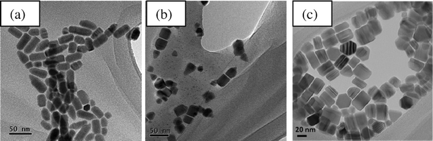 | ||
Fig. 6 TEM images of CdSe nanocrystals synthesized with DDPA-to-Cd mole ratios of (a) 3![[thin space (1/6-em)]](https://www.rsc.org/images/entities/char_2009.gif) :1, (b) 4:1 and (c) 5:1. :1, (b) 4:1 and (c) 5:1. | ||
Influence of the Cd-to-E mole ratio
The Cd-to-E mole ratio was another important factor that influenced the morphology of the resulting nanocrystals. It was found that decreasing the Cd-to-E mole ratio can lead to a decrease in the highest aspect ratio of the CdE nanocrystals. A possible explanation is that the more E precursor present in the initial stage (lower Cd-to-E mole ratio), the faster the nucleation process occurs and more nuclei are formed during nucleation. This trend is true for CdE nanocrystals. On the other hand, increasing the mole ratio has different effects on CdS, CdSe and CdTe. During the synthesis of CdS nanocrystals we increased the initial Cd-to-S mole ratio to 1:0.5 and obtained a mixture of tiny particles and nanowires with different lengths. Some of the nanowires were longer than 1 μm. There were some tiny particles observed which had no chance to grow due to an earlier depletion of the monomer. Thus, growth is limited by the amount of S. In the synthesis of CdSe and CdTe nanocrystals, different results were obtained. When the mole ratio is equal to 1:0.5, CdTe nanorods with a length of 25 nm and also branched nanocrystals were produced. With a further increase in the mole ratio to 1:0.25, mainly spherical shape CdTe nanocrystals with a diameter of 7 nm were found. The color change from colorless to dark brown after the initial injection takes around 8 min for the Cd-to-Te mole ratio of 1:0.25, 3.5 min for 1:0.5 and 2 min for 1:1. This is due to insufficient Te monomers being left after fast nucleation. In addition, although using a higher Cd-to-E mole ratio can help to get high aspect ratio CdS nanocrystals, the final CdS nanocrystals are usually mixed with many unreacted complexes and tiny particles. These will affect the ligand exchange and charge transport in photovoltaic applications.46 Thus, it was proposed for the synthesis of pure and high aspect ratio CdE nanocrystals that the Cd-to-E mole ratio would be 1:1.
Influence of the precursor concentration
The monomer concentration in the solution is thought to play a key role for the determination and evolution of the morphology of the final nanocrystals.28 In previous studies, as the precursor concentration was increased, the morphology of the nanocrystals changed from dots to rice grains, short rods, long rods and finally branched structures.28,41 In these studies, a different trend was observed. We found that in order for CdE nanowires to grow longer, a high precursor concentration is required. During the synthesis of CdS nanowires, reducing the precursor concentration by half results in the formation of shorter nanowires. The length of the nanowires ranged from 50 to 150 nm and the diameter was 3.4 nm. When the precursor concentration is doubled, the reaction yields shorter nanowires mixed with short rods and dots. We propose that the reason is due to the higher number of nuclei at the initial stage of the reaction. During the synthesis of CdSe nanowires, we found that when the precursor concentration was doubled, the reaction yielded nanowires with nearly monodisperse diameters of 8 nm and lengths of 220 nm. However, a further increase in the precursor concentration showed an adverse effect on the distribution of the length, diameter and aspect ratio of the nanocrystals. The length of the nanocrystals ranged from 20 to 300 nm and the diameter ranged from 5 to 12 nm. A higher precursor concentration may result in either longer nanowires or branches.28,41 This is the case for CdSe, but not for CdTe. We found that doubling the precursor concentration yielded CdTe nanorods and branches with a length of less than 50 nm and a diameter of 3.4 nm (see Fig. 7). Increasing the precursor concentration of the highly reactive component will result in more nucleation at the start of the reaction consuming the precursors necessary for growth. Therefore, increasing the precursor concentration is not an effective way to produce high aspect ratio CdTe nanocrystals. Other parameters, such as the injection process, may affect the nucleation and growth more substantially and will be presented in the next section.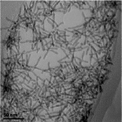 | ||
| Fig. 7 TEM images of CdTe nanocrystals synthesized with a double precursor concentration. | ||
Influence of the injection process
Constant supply and replenishment of the monomer is thought to be an important synthesis strategy.47 As discussed above, the monomer concentration in the reaction is an important factor. The injection process was found to be able to control the monomer concentration, thus affecting the nanocrystal growth model. In these studies, the effect of the precursor injection process on the morphology of the nanocrystals was investigated while keeping other parameters constant. It was found that a different final nanocrystal morphology was obtained when using different injection process, including single fast injection, single continuous injection and multiple injections. For example, in the synthesis of CdS nanowires, we found that a single fast injection generates short nanowires. Their length ranged from a few tens of nanometers to 200 nm, and their diameter was 3.7 nm. This is because the single injection introduced all the sulphur monomer at once, resulting in a nucleation burst. A rapid and intense nucleation burst will consume the monomer very quickly and result in a larger number of nuclei than for multiple injections. These nuclei consumed most of the monomer in a short time. The remaining low monomer concentration cannot sustain the anisotropic growth regime for a long time, resulting in a lower aspect ratio, as we discussed earlier. When multiple injections at 2 min intervals are carried out, the nanocrystals formed are nearly monodisperse nanowires with very high aspect ratios (see Fig. 1a). This is because multiple injections regularly replenish the monomer concentration and hence this condition provides a relatively stable growth environment with a high monomer concentration.23,37,41 In the synthesis of CdSe nanowires, a similar trend was observed when using a single fast injection and multiple injections (4 times × 2 min interval × 2 min injection duration). When the injection interval was increased from 2 min to 4 min or even longer, the length of the nanocrystals was decreased while the diameter remained constant. CdSe nanowires were obtained with a length of around 170 nm and a poor size distribution. The long interval between the multiple injections was not able to maintain a high monomer concentration in the solution which is thought to be a prerequisite for anisotropic growth with a high aspect ratio.23,28In the synthesis of CdTe nanowires, there is a big difference in morphology between a single continuous injection and multiple injections (4 times × 2 min interval × 2 min injection duration). Using multiple injections, CdTe nanorods with a length of less than 50 nm and a diameter of 6.1 nm were produced (see Fig. 8a). Although a multiple injection process can periodically replenish the monomer, the faster cleavage rate of P = Te compared to P = Se or P = S leads to a high number of nuclei in the reaction. These nuclei grow to larger crystals by consuming the monomers between intervals. Thus there is a relatively low monomer concentration and a variable growth environment, which cannot sustain the anisotropic growth regime for a long time, resulting in a lower aspect ratio. However, when a single continuous injection is carried out, CdTe nanowires with a high aspect ratio can be produced (see Fig. 8b–d). It was found that changing the duration of the injection can change the aspect ratio of the nanocrystals substantially. When the duration of the injection is 12 min, CdTe nanorods were obtained with a length of around 83 nm and a diameter of 7.1 nm (see Fig. 8b). Increasing the injection duration to 18 min produces CdTe nanowires with a length of 119 nm and the diameter remaining constant (see Fig. 8c). When the injection duration is increased to 28 min, CdTe nanowires with the highest aspect ratios were obtained (see Fig. 2b). On further increasing the injection duration to 36 min, the average length of the CdTe nanowires decreased slightly from 210 nm to 180 nm while the diameter increased slightly from 7.5 nm to 9.8 nm. Some nanowires have lengths of more than 450 nm. We believed that with a moderately long duration a high monomer concentration was maintained in the reaction by continuously refreshing the monomer. In addition, it can be seen that the number of branches increases with increasing injection duration (see Fig. 2b and Fig. 8c–d). This is possible due to the relatively low monomer concentration during long duration injection (36 min) compared to shorter injection times (18 or 28 min). The monomer concentration over course of the reaction is now limited by the amount of Te. Thus, if the overall rate of cleavage, nucleation and growth is slow, multiple injections that can separate nucleation and growth will be the most effective way to control anisotropic growth. If the rate is fast, a single continuous injection which can help maintain a good balance in supply of monomers is effective. This implies that the injection process has to depend on the reactivity of the element in the synthesis of nanowires in solution.
 | ||
| Fig. 8 TEM images of CdTe nanocrystals synthesized using (a) multiple injections (4 times with 2 min duration at 2 min intervals) and a single continuous injection with different durations: (b) 12 min, (c) 18 min and (d) 36 min. | ||
Influence of the reaction temperature
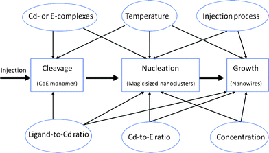
Using an appropriate reaction temperature is one of the key parameters in obtaining control over nanocrystal growth.47 The reaction temperature was found to be another factor affecting the cleavage rate. This is because regardless of growth mechanism, the cleavage of the P = E bond is a thermodynamic process. On top of this, stability and diffusion rate of the Cd and E complexes, as well as the binding strength of the ligands to the growing nanocrystals surface, are all strongly temperature dependent.47 Thus, the temperature dependence of the aspect ratio can be seen to be similar to the concentration dependence.41 In the synthesis of CdS and CdSe nanowires, we found that the optimal reaction temperature is 310 °C. A lower reaction temperature results in a lower cleavage rate and a lower monomer concentration in the solution. As a result, the lower monomer concentration does not favor growth along the c-axis of a wurtzite structure. When the reaction temperature was increased to above 320 °C, CdS nanowires with a higher aspect ratio and branched structures are obtained. This result was consistent with previous studies.25 In that study, Kang et al. also found that the growth rate along the c-axis of the wurtzite structure is temperature-dependent. In the synthesis of CdSe and CdTe nanocrystals, a similar trend was observed at a moderately low temperature (see Fig. S4† for different temperature effects on CdTe nanocrystals). We observed that as the reaction temperature increased from 250 to 300 °C, the aspect ratio of the CdTe nanocrystals also increased. However, further increasing the reaction temperature to 322 °C resulted in a lower aspect ratio. This was different for CdS nanocrystals. CdTe nanowires with a length of 73 nm and a diameter of 6.7 nm were produced. It was proposed that cleavage is a thermodynamic process and can be accelerated by a increased reaction temperature. This is because increasing the temperature can decrease the stability of the (TOP = E)-Cd-phosphonic acid complexes.47 As a result there is a fast cleavage rate and a higher number of nuclei in the reaction which is not good for anisotropic growth. Furthermore, too high a temperature can also decrease the binding effect of the surfactants on the CdTe nanocrystal surface. Therefore, we proposed that optimal reaction temperature for CdTe nanowires is 300 °C.A summary of the effects of the reaction parameters on the growth of nanocrystals is presented in Fig. 9. (1) The Cd-complexes and E-complexes affect both the cleavage and nucleation processes. It was found that the Cd-complexes and E-complexes mainly affect the cleavage of the P = E double bond.39 The cleavage is supposed to be the process which leads to the formation of CdE monomers, while the rate of this cleavage mainly affects nucleation. (2) The ligand-to-Cd mole ratio mainly affects the reactivity of Cd complexes. With a higher phosphonic acid-to-Cd mole ratio, the accessibility of the phosphine for the Cd is reduced and thus results in a slow cleavage rate of the P = E double bond. This will further affect nucleation and growth. (3) The Cd-to-E mole ratio mainly affects the amount of E precursor present in the solution. This will affect the number of nuclei and nucleation rate. The Cd-to-E mole ratio also affects the dispersity of the final products. (4) The precursor concentration can influence the growth mode of nanocrystals by affecting both nucleation and growth.28,37 Based on the effective monomer model, nanocrystal growth goes through three stages: 1D growth stage, 3D growth stage and 1D to 2D ripening stage as the effective monomer concentration decreases.28,37 At higher monomer concentrations, nanocrystals may follow the 1D growth mode, while at lower concentrations, the growth follows the 1D/2D growth mode, in between, the growth follows the 3D model. (5) The injection process will also affect the monomer concentration in the solution. A fast injection process produces a large number of nuclei in the reaction, which will consume the monomer in a short time and is not favorable for high aspect ratio growth. (6) The reaction temperature affects three stages: the cleavage, nucleation and growth of the nanocrystals. This is because the cleavage is a thermodynamic process and thus affected by the reaction temperature. The temperature dependence can also be seen as another form of the concentration dependence.41 On the basis of our results, the optimum conditions for the growth of high aspect ratio CdE nanowires are summarized in Table 1.
 | ||
| Fig. 9 Scheme showing the effects of various reaction parameters on nanocrystal growth. | ||
| Ligand for Cd complex | Ligand for E complex | Ligand-to-Cd mole ratio | Cd-to-E mole ratio | Concentration (mol kg−1) | Injection process | Reaction temp. (°C) | TOP = E complexes formation conditions | Reaction time (after final injection) | |
|---|---|---|---|---|---|---|---|---|---|
| Cds | ODPA | TOP | 1:2 |
1:1 |
0.17 | Multiple | 310 | Stirring 30 min at room temp. | 2 h |
| CdSe | DDPA | TOP | 1:2 |
1:1 |
0.35 | Multiple | 310 | Stirring 1 h at room temp. | 30 min |
| CdTe | DDPA | TOP | 1:2 |
1:1 |
0.15 | Single continuous | 300 | Stirring 1.5 h at 200 °C | 15 min |
Growth mechanism
For the synthesis of CdE nanocrystals, a series of time-dependent studies of the growth was carried out. In previous studies,26,27 we presented time-dependent studies of CdS and CdSe nanocrystals. On the basis of these time-dependent studies, the effective monomer model28,37 is used to explain the shape evolution of CdE nanocrystals. This model suggests that the growth of anisotropic nanocrystals mainly depends upon the effective monomer concentration. A time-dependent study of the growth of CdTe nanocrystals is shown in Fig. 10. In this study, a single continuous injection with a duration of 28 min was used. It can be seen that after a 7 min injection of TOP = Te solution, long nanowires mixed with branches are formed. The length of the nanowires ranges from a few tens to 200 nm and the diameter is 4.6 nm (see Fig. 10a). With more precursor subsequently injected and the reaction proceeding, these thin nanowires grew longer and slightly thicker. After a 14 min injection of precursor, the length of the nanowires grew to 210 nm and their diameter increased to 5.2 nm (see Fig. 10b). At 21 min, the length and diameter of nanowires grew to 150–300 nm and 6.8 nm, respectively (see Fig. 10c). It can be seen that there are some tiny dots in the Fig. 10a–c. These tiny dots disappeared after a few minutes of final injection. Fifteen minutes after the injection, the average length of the nanowires was about 210 nm and the diameter was 7.5 nm. The increase in the length and diameter was due to continuous replenishment of the precursors. The reason for the high aspect ratio CdE nanowires is due to a good balance between the kinetic and the thermodynamic growth regimes. This strongly affects the final morphology of the nanocrystals. Anisotropic growth of nanocrystals along their c-axis is favored under a kinetic growth regime if a high precursor concentration is present.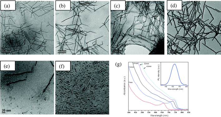 | ||
| Fig. 10 Time-dependent TEM images of CdTe nanocrystals synthesized with a single continuous injection at: (a) 7 min, (b) 14 min, (c) 21 min and (d) 43 min. Evidence of oriented attachment from (e) CdTe and (f) CdS nanocrystals. (g) Time-dependent UV-Vis absorption spectra of CdTe nanocrystals. (inset: PL spectrum after 21 min). | ||
Although the effective monomer model can explain the shape evolution of CdE nanocrystals, we observed that the nanocrystals may follow the oriented attachment mechanism in some cases (see Fig. 10e–f and Fig. S5† for the additional TEM images) as well as previous images.27 In Fig. 10e, there are lots of tiny nanodots accumulated at the ends of the CdTe nanowires. It can be seen that the nanowires were not well grown. The image is taken after 19 min, which is during the initial stage of a single injection. We think that this is strong evidence of oriented attachment. This is because a single continuous injection for CdTe provides a relatively long time for the agglomeration and fusion of these tiny dots. With the new precursor injected, these tiny nanodots grow and attach to the previously formed nanowires (see Fig. 10e). As the reaction progresses, these dots fuse and became part of the nanocrystals.48 A similar phenomenon was also observed in the synthesis of CdS and CdSe nanowires (see Fig. 10f and ref. 27). The most probable reason for the oriented attachment is due to the presence of a dipole moment49 or higher surface reactivity50 of these tiny nanocrystals. UV-Vis absorption spectra of the CdTe nanocrystals at different stages of growth and a typical photoluminescence spectrum are shown in Fig. 10g. It can be seen that the first exciton absorption is located at around 660–750 nm. Its intensity gradually increases and the peak center is red shifted as the reaction proceeds. This shift is consistent with the increase in diameter of the nanowires.37,43,44 The reactivity of the precursor may have an implication on the chemical composition of the wires. Next we will look at Raman studies of these wires.
Raman study
A typical Raman spectrum from 100 cm−1 to 700 cm−1 for CdSe nanowires excited with 532 nm light is shown in Fig. 11, which was collected from as prepared CdSe nanowires dispersed on an ITO-coated glass substrate. The laser power was 1.5 mW. The Raman spectrum can be fitted with multiple Lorentzian peaks as shown in the inset, giving Raman shifts at 171 cm−1, 204 cm−1, 207 cm−1, 387 cm−1, 414 cm−1 and 620 cm−1. A Raman study of CdSe nanostructures has been reported.51–53 Accordingly, we can assign the prominent Raman peaks of 171 cm−1, 207 cm−1, 414 cm−1, 620 cm−1 as transverse optical (TO), longitudinal optical (LO), 2LO and 3LO phonons, respectively. A surface optical (SO) phonon with a frequency between those of TO and LO modes has been reported in CdSe nanospheres and CdSe quantum dots in a glass matrix.54 The SO mode is determined by the dielectric properties of the materials on both sides as well as the morphology of the object, as identified by Xiong et al. in GaP and ZnS nanowires.55,56 A symmetry breaking mechanism associated with the surface roughness is needed to “activate” the SO mode. In our study, the surface of some CdSe nanowires is not so smooth (see Fig. S6†). It's reasonable to assign the 204 cm−1 peak to SO and the 387 cm−1 peak to the combination band TO+LO, which was also observed in the CdSe nanospheres.54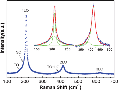 | ||
| Fig. 11 Raman spectrum for CdSe nanowires excited by light of wavelength 532 nm. The inset shows segment display fitting. The blue dots are the experimental data, the red line is the fitted result and the green lines are the fitted Lorentzian peaks. The 3-peak fit gives a better result than the 2-peak fit as shown in the inset. | ||
Fig. 12 shows a Raman spectrum for as prepared CdTe nanowires excited by 532 nm wavelength light. The laser power was kept at 1.5 mW. The spectrum (red circles) was fitted with six Lorentzian peaks (green) located at 93 cm−1, 122 cm−1, 140 cm−1, 163 cm−1, 220 cm−1 and 265 cm−1. The result is shown as the blue line. Amirtharaj et al.57 have identified that the peaks located at 93 cm−1, 122 cm−1 and 140 cm−1 are from trigonal Te. The 122 cm−1 peak is due to a phonon with A1 symmetry and the 93 cm−1 and 140 cm−1 peaks originate from phonons with an E symmetry.58 However, the 140 cm−1 peak could also be assigned to the TO phonon in CdTe because it is very close to one as reported.57,59 According to Raman studies of CdTe,57,60,61 the peak located at 163 cm−1 can be assigned to the LO phonon of CdTe, in spite of a difference from 171 cm−1 and 167 cm−1 reported by Islam et al.61 and Amirtharaj et al.57 respectively. To the best of our knowledge, there have been no reports of the assignment for the broad bands located at 220 cm−1 and 265 cm−1, which probably originate from combination bands and we tentatively assign them to the overtones of E and A1 modes in Te. A high concentration of tellurium exists in the as-prepared CdTe nanowires, as shown by the Raman study. Similar phenomena were reported in CdTe film synthesized through the liquid-phase epitaxy method61 as well as the surface of single crystal CdTe in bulk form.57 It could be argued that the appearance of Te may result from laser heating. However, a similar spectrum was obtained even when the power of the laser spot was decreased to 0.02 mW. One possible explanation could be that the free energy of Te is smaller than that of CdTe and thus Te crystals can easily form during the synthesis of CdTe. However, further study is still needed to confirm this. One implication for this is that the surface property of the nanowires may not be as expected. Isolated elemental domains (Te) are formed or precipitated on the surface of nanowires, it may affect their applications in optoelectronic devices since its elemental properties are different from its compound properties.
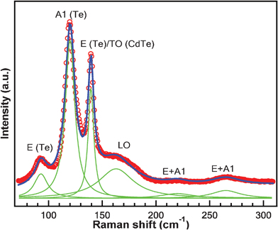 | ||
| Fig. 12 Raman spectrum and multi-Lorentzian fitting result for as-prepared CdTe nanowires under 532 nm excitation. The fitted peaks are assigned to phonons from Te and CdTe as denoted. | ||
Conclusions
In summary, CdE (E = S, Se and Te) nanowires were successfully synthesized using a catalyst-free solution-based method. We demonstrate good control over the synthesis of CdE nanowires using the hot coordinating solvents method. In this paper, we present our very recent results on the synthesis of CdTe nanowires and summarize our understanding of the effects of reaction parameters on the growth of CdE nanowires. We systematically studied and discussed several reaction parameters, including ligands for Cd-complexes and E-complexes, ligand-to-Cd mole ratio, Cd-to-E mole ratio, precursor concentration, the injection process and the reaction temperature. We further summarized the effects of these parameters on the growth of high aspect ratio nanocrystals. Optimum conditions for the growth of CdE nanowires were also proposed. Finally, the growth mechanism was also proposed and discussed. On top of the effective monomer model, which can mostly explain the shape evolution of CdE nanocrystals, the oriented attachment mechanism was also proposed. Furthermore, a Raman study shows the presence of SO in CdSe surfaces due to the rough surface and a higher concentration of tellurium on the surface of the CdTe nanowires. We hope that this paper can serve as a guide for the synthesis of group II–VI nanowires in the future.References
- G. Zheng, X. P. A. Gao and C. M. Lieber, Nano Lett., 2010, 10, 3179 CrossRef CAS.
- Y. Huang, X. Duan, Y. Cui, L. J. Lauhon, K.-H. Kim and C. M. Lieber, Science, 2001, 294, 1313 CrossRef CAS.
- G. Yu, A. Cao and C. M. Lieber, Nat. Nanotechnol., 2007, 2, 372 CrossRef CAS.
- J. P. Colinge, C.W. Lee, A. Afzalian, N. D. Akhavan, R. Yan, I. Ferain, P. Razavi, B. O'Neill, A. Blake, M. White, A. M. Kelleher, B. McCarthy and R. Murphy, Nat. Nanotechnol., 2010, 5, 225 CrossRef CAS.
- M. Law, L. E. Greene, J. C. Johnson, R. Saykally and P. Yang, Nat. Mater., 2005, 4, 455 CrossRef CAS.
- B. Tian, X. Zheng, T. J. Kempa, Y. Fang, N. Yu, G. Yu, J. Huang and C. M. Lieber, Nature, 2007, 449, 885 CrossRef CAS.
- C. M. Lieber, MRS Bull., 2003, 28, 486 CrossRef CAS.
- P. Yang, R. Yan and R. Fardy, Nano Lett., 2010, 10, 1529 CrossRef CAS.
- Y. Ye, L. Dai, T. Sun, L. P. You, R. Zhu, J. Y. Gao, R. M. Peng, D. P. Yu and G. G. Qin, J. Appl. Phys., 2010, 108, 044301 CrossRef.
- D. J. Milliron, S. M. Hughes, Y. Cui, L. Manna, J. Li, L. W. Wang and A. P. Alivisatos, Nature, 2004, 430, 190 CrossRef CAS.
- D. D. Fanfair and B. A. Korgel, Chem. Mater., 2007, 19, 4943 CrossRef CAS.
- J. Puthussery, A. Lan, T. H. Kosel and M. Kuno, ACS Nano, 2008, 2, 357 CrossRef CAS.
- M. C. Kum, Y. Y. Bong, W. R. Young, K. N. Bozhilov, W. Chen, A. Mulchandani and N. V. Myung, Nanotechnology, 2008, 19, 325711 CrossRef.
- Z. Tang, N. A. Kotov and M. Giersig, Science, 2002, 297, 237 CrossRef CAS.
- Y. Wang, Z. Tang, S. Tan and N. A. Kotov, Nano Lett., 2005, 5, 243 CrossRef CAS.
- H. Bao, E. Wang and S. Dong, Small, 2006, 2, 476 CrossRef CAS.
- N. Wang, Y. Cai and R. Q. Zhang, Mater. Sci. Eng., R, 2008, 60, 1 CrossRef.
- N. Pradhan, H. Xu and X. Peng, Nano Lett., 2006, 6, 720 CrossRef CAS.
- C. Pacholski, A. Kornowski and H. Weller, Angew. Chem., Int. Ed., 2002, 41, 1188 CrossRef CAS.
- A. B. Panda, S. Acharya and S. Efrima, Adv. Mater., 2005, 17, 2471 CrossRef CAS.
- K. S. Cho, D. V. Talapin, W. Gaschler and C. B. Murray, J. Am. Chem. Soc., 2005, 127, 7140 CrossRef CAS.
- C. B. Murray, D. J. Noms and M. G. Bawendi, J. Am. Chem. Soc., 1993, 115, 8706 CrossRef CAS.
- X. Peng, L. Manna, W. D. Yang, J. Wickham, E. Scher, A. Kadavanich and A. P. Alivisatos, Nature, 2000, 404, 59 CrossRef CAS.
- F. Wang, A. Dong, J. Sun, R. Tang, H. Yu and W. E. Buhro, Inorg. Chem., 2006, 45, 7511 CrossRef CAS.
- C. C. Kang, C. W. Lai, H. C. Peng, J. J. Shyue and P. T. Chou, Small, 2007, 3, 1882 CrossRef CAS.
- L. F. Xi, W. X. W. Tan, C. Boothroyd and Y. M. Lam, Chem. Mater., 2008, 20, 5444 CrossRef CAS.
- L. F. Xi and Y. M. Lam, Chem. Mater., 2009, 21, 3710 CrossRef CAS.
- X. Peng, Adv. Mater., 2003, 15, 459 CrossRef CAS.
- M. Afzaal and P. O'Brien, J. Mater. Chem., 2006, 16, 1597 RSC.
- P. Peng, D. J. Milliron, S. M. Hughes, J. C. Johnson, A. P. Alivisatos and R. J. Saykally, Nano Lett., 2005, 5, 1809 CrossRef CAS.
- M. Kazes, D. Y. Lewis, Y. Ebenstein, T. Mokari and U. Banin, Adv. Mater., 2002, 14, 317 CrossRef CAS.
- M. S. Gudiksen, K. N. Maher, O. Lian and H. Park, Nano Lett., 2005, 5, 2557 CrossRef.
- N. P. Gaponik, D. V. Talapin, A. L. Rogach and A. Eychmuller, J. Mater. Chem., 2000, 10, 2163 RSC.
- M. Gao, C. Lesser, S. Kirstein, H. Mohwald, A. L. Rogach and H. Weller, J. Appl. Phys., 2000, 87, 2297 CrossRef CAS.
- R. S. Singh, V. K. Rangari, S. Sanagapalli, V. Jayaraman, S. Mahendra and V. P. Singh, Sol. Energy Mater. Sol. Cells, 2004, 82, 315 CrossRef CAS.
- D. Verma, A. R. Rao and V. Dutta, Sol. Energy Mater. Sol. Cells, 2009, 93, 1482 CrossRef CAS.
- Z. A. Peng and X. G. Peng, J. Am. Chem. Soc., 2001, 123, 1389 CrossRef CAS.
- L. Manna, D. J. Milliron, A. Meisel, E. C. Scher and A. P. Alivisatos, Nat. Mater., 2003, 2, 382 CrossRef CAS.
- H. Liu, J. S. Owen and A. P. Alivisatos, J. Am. Chem. Soc., 2007, 129, 305 CrossRef CAS.
- P. D. Cozzoli, L. Manna, L. M. Curri, S. Kudera, C. Giannini, M. Striccoli and A. Agostiano, Chem. Mater., 2005, 17, 1296 CrossRef CAS.
- Z. A. Peng and X. G. Peng, J. Am. Chem. Soc., 2002, 124, 3343 CrossRef CAS.
- http://www.science-and-fun.de/tools/ .
- F. Shieh, A. E. Saunders and B. A. Korgel, J. Phys. Chem. B, 2005, 109, 8538 CrossRef CAS.
- A. L. Washington II and G. F. Strouse, J. Am. Chem. Soc., 2008, 130, 8916 CrossRef.
- L. F. Xi, W. X. W. Tan, K. S. Chua, C. Boothroyd and Y. M. Lam, Thin Solid Films, 2009, 517, 6430 CrossRef CAS.
- J. Y. Lek, L. F. Xi, B. E. Kardynal, L.H. Wong and Y. M. Lam, ACS Appl. Mater. Interfaces, 2011, 3, 287 CAS.
- Y. Yin and A. P. Alivisatos, Nature, 2005, 437, 664 CrossRef CAS.
- H. Cao, G. Wang, S. Zhang, X. Zhang and D. Rabinovich, Inorg. Chem., 2006, 45, 5103 CrossRef CAS.
- A. Shanbhag and N. A. Kotov, J. Phys. Chem. B, 2006, 110, 12211 CrossRef.
- F. S. Riehle, R. Bienert, R. Thomann, G. A. Urban and M. Kruger, Nano Lett., 2009, 9, 514 CrossRef CAS.
- R. Venugopal, P. I. Lin, C. C. Liu and Y. T. Chen, J. Am. Chem. Soc., 2005, 127, 11262 CrossRef CAS.
- R. Beserman, Solid State Commun., 1977, 23, 323 CrossRef CAS.
- A. K. Arora and A. K. Ramdas, Phys. Rev. B, 1987, 35, 4345 CrossRef CAS.
- M. C. Klein, F. Hache, D. Ricard and C. Flytzanis, Phys. Rev. B: Condens. Matter, 1990, 42, 11123 CrossRef CAS.
- R. Gupta, Q. Xiong, G. D. Mahan and P. C. Eklund, Nano Lett., 2003, 3, 1745 CrossRef CAS.
- Q. Xiong, J. Wang, O. Reese, L. C. L. Y. Voon and P. Eklund, Nano Lett., 2004, 4, 1991 CrossRef CAS.
- P. M. Amirtharaj and F. H. Pollak, Appl. Phys. Lett., 1984, 45, 789 CrossRef CAS.
- A. S. Pine and G. Dresselhaus, Phys. Rev. B: Solid State, 1971, 4, 356 CrossRef.
- S. Perkowitz and R. H. Thorland, Phys. Rev. B: Solid State, 1974, 9, 545 CrossRef CAS.
- A. Mooradian and G. B. Wright in Proceedings of the Ninth International Conference on the Physics of semiconductors, Nauka Publishing House,Leningrad, Moscow, 1968 Search PubMed.
- S. S. Islam, S. Rath, K. P. Jain, S. C. Abbi, C. Julien and M. Balkanski, Phys. Rev. B: Condens. Matter, 1992, 46, 4982 CrossRef CAS.
Footnote |
| † Electronic supplementary information (ESI) available: XRD and HRTEM image of CdTe nanowires (Fig. S1 and S2). TEM images of CdTe nanocrystals synthesized with a DDPA-to-Cd mole ratios equal to 2.5:1 (Fig. S3) and at different temperatures (Fig. S4). Additional TEM images show evidence of oriented attachment (Fig. S4 and S5). TEM image of CdSe nanowires with rough surface (Fig. S6). See DOI: 10.1039/c2ra20060k |
| This journal is © The Royal Society of Chemistry 2012 |