Morphology of SiC nanowires grown on the surface of carbon fibers
Elena
Kudrenko
*ab,
Vladimir
Roddatis
b,
Andrey
Zhokhov
a,
Irina
Zverkova
a,
Igor
Khodos
c and
Gennady
Emelchenko
a
aInstitute of Solid State Physics RAS, 142432 Chernogolovka, Russia. E-mail: lenak@issp.ac.ru; Fax: +7-496-522-81-60; Tel: +7-496-522-82-74
bNational Research Centre Kurchatov Institute, 123182 Moscow, Russia
cInstitute of Microelectronics Technology and High Purity Materials RAS, 142432 Chernogolovka, Russia
First published on 27th April 2012
Abstract
SiC nanowires (NWs) with diameters of 20–200 nm and lengths from tens to hundreds of micrometers have been synthesized by the carbothermal reduction of colloidal silica. The morphology and microstructure of NWs have been studied in detail by electron microscopy techniques. SiC NWs have been found to be hexagonal prisms, “bamboo-like” nanorods and nanobelts. The NWs with a [111] growth axis are hexagonal prism nanorods, while the nanobelts have growth directions varying from [110] to [113]. It has been found that NW growth proceeds in two stages. Initially, SiC crystallites grow on the carbon fiber surface. These crystallites serve as seeds, on which the SiC NWs nucleate and grow. The crystallites containing microtwins and stacking faults (SFs) with a preferential [111] growth direction give rise to the growth of nanorods, while the nanobelts start growing on the (111) facets of relatively perfect crystallites. Wires with core (SiC)–shell (SiO2) structure have been obtained under special temperature treatment in air. The core–shell structure has been confirmed by transmission electron microscopy (TEM) and energy-dispersive X-ray spectroscopy (EDX) mapping techniques.
1. Introduction
Silicon carbide nanowires (NWs) have received much attention due to their prominent characteristics, such as high mechanical strength, high thermal conductivity and excellent chemical inertness.1 Enhanced photocatalytic properties have been found in semiconductor nanowires of silicon carbide coated with an oxide layer.2 SiC NWs can be used to best advantage as elements of nanoelectronic devices under high temperature environments. Various methods have been applied to produce SiC NWs such as chemical vapor deposition (CVD),3 arc discharge,4 carbothermal reactions using carbon nanotubes,5 “bamboo-like” nanorods6 and activated carbon,7 laser sputtering,8etc.9–15 Carbothermal reduction of silica is the most useful method of SiC NW synthesis owing to its efficiency and simplicity. It is well known that the carbon source significantly affects the reaction rate as well as the morphology and size of synthesized SiC wires.16 Both silica (SiO2) powder and silicon monoxide (SiO) are used as silicon sources in carbothermal reactions.2The morphology of SiC nanocrystals is determined by the synthesis methods. The successful formation of periodically twinned NWs,17 helical NWs,18 wires with periodical bulbs of SiO2 coatings,19 nanotubes,20 three-dimensional nanonets,21 S- and Y-shaped bicrystals22–25 and bicrystalline nanobelts25 has been reported. It should be noted that the [111] growth direction is typical of most NWs including NWs obtained by the carbothermal reduction of silica.2,5–7,17,23,24,26–28 In the case of bicrystalline NWs growth has been observed along [110], [112] or [113] crystallographic axes.22–25
Despite the numerous studies on the synthesis methods, the structure and properties of SiC NWs, little attention is paid in the literature to the mechanisms of NW growth and the structural transformation during the growth process.
We report the results of the investigation of silicon carbide NWs obtained by the carbothermal reduction of SiO2. A combination of analytical electron microscopy techniques such as field-emission electron microscopy (FESEM), high-resolution transmission electron microscopy (HRTEM), energy-dispersive X-ray spectroscopy (EDX) and X-ray powder diffraction (XRD) have been used to study the morphology types and growth stages of SiC NWs in detail.
2. Experimental
The SiO2 spherical particles were produced by the hydrolysis of tetraethylorthosilicate (TEOS) in ethanol solution in the presence of ammonium hydroxide.29,30 The use of an acidic medium results in the formation of small size (∼10 nm) particles. The SiO2-particles suspension was mixed with a water solution of colloid graphite to obtain excess carbon content with a ratio of C![[thin space (1/6-em)]](https://www.rsc.org/images/entities/char_2009.gif) :SiO2 > 1. After ultrasonic treatment and intensive mixing with a magnetic stirrer, the suspension was dried and placed into a graphite crucible which was covered with carbon felt with a central through hole for outflow of the synthesized products and localization of the temperature gradient. The synthesis was carried out in an induction furnace in an argon atmosphere (0.5 atm) at 1450 °C for 1 h. The reaction product was a light blue fluffy layer deposited on the outer side of the felt around its central hole. The phase composition of the synthesized product was characterized by XRD using a Siemens D-500 diffractometer with CoKα radiation. The sample morphology has been examined with a Zeiss Supra 50VP FESEM equipped with an EDX spectrometer. The microstructure of the sample has been studied by transmission electron microscopy (TEM), the selected area electron diffraction pattern (SAED) using a Jeol JEM-100CX and HRTEM using Titan 80-300 and Jeol JEM-2100.
:SiO2 > 1. After ultrasonic treatment and intensive mixing with a magnetic stirrer, the suspension was dried and placed into a graphite crucible which was covered with carbon felt with a central through hole for outflow of the synthesized products and localization of the temperature gradient. The synthesis was carried out in an induction furnace in an argon atmosphere (0.5 atm) at 1450 °C for 1 h. The reaction product was a light blue fluffy layer deposited on the outer side of the felt around its central hole. The phase composition of the synthesized product was characterized by XRD using a Siemens D-500 diffractometer with CoKα radiation. The sample morphology has been examined with a Zeiss Supra 50VP FESEM equipped with an EDX spectrometer. The microstructure of the sample has been studied by transmission electron microscopy (TEM), the selected area electron diffraction pattern (SAED) using a Jeol JEM-100CX and HRTEM using Titan 80-300 and Jeol JEM-2100.
3. Results and discussion
3.1. General characteristics of synthesized wires
The XRD pattern of the synthesized product is shown in Fig. 1. All the strong diffraction peaks can be indexed in the 3C-SiC structure. Hence, the 3C-polytype is used for further description of the SiC NWs structure. The low intensity peaks marked by X are due to stacking faults (SFs) and twins in the sample. The broad peaks with low-intensity satellites labeled C come from the carbon felt material.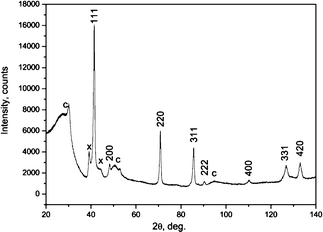 | ||
| Fig. 1 The XRD spectrum of the SiC NWs on the carbon felt substrate: indexed peaks, SiC-3C phase, X-peaks due to high density SFs, C, carbon with low crystalline graphite content. | ||
Fig. 2a shows the FESEM image of the general view of the synthesis product. It is seen that the product consists of wires from 20 to 200 nm in diameter and up to several tens of microns in length. FESEM images in Fig. 2b–e show that the NWs have different types of morphology. From the TEM images in Fig. 2f–i it follows that the wires have a pronounced striped structure which points to the presence of SFs and twins. By and large, three types of NW morphology can be distinguished: nanorods with hexagonal prismatic morphology (Fig. 2b and g); “bamboo-like” nanorods (Fig. 2c and f) and nanobelts (Fig. 2d, e and h) with a rectangle-like cross-section (Fig. 2d and e) and typical aspect ratio 10 (Fig. 2e). In rare cases, Y-shaped bicrystalline wires31 are observed as shown in Fig. 2i. The bicrystal “trunk” is composed of two wires connected along the (111)-3C twinning plane which then branch at 70° corresponding to the angle between the (111)-type planes in the cubic system. A more detailed description of the NW-type structures is given below.
 | ||
| Fig. 2 The general view FESEM image of the NWs (a); (b) and (c) FESEM images of single hexagonal prism-shaped and “bamboo-like” nanorods, respectively; (d) and (e) FESEM images of nanobelts; (f)–(i) TEM bright-field images of the NW types. | ||
3.2. Nucleation and growth of SiC NWs
The FESEM image of a single carbon fiber after SiC NW synthesis is shown in Fig. 3a. The fiber surface shows light areas and outgrowing wires. More detailed pictures of such light areas (Fig. 3d–f) reveal that they are composed of SiC crystallites with different morphology and SiC NWs. The crystals and wires show a striped microstructure (Fig. 3e and f) which reflects the presence of SFs and microtwins which is typical for polytypic structures. EDX mapping of the elements on the surface of a single fiber (Fig. 3a) is represented in Fig. 3b and c. It is seen that silicon is present mainly in the light regions of the image (Fig. 3a). Therefore, the observed crystallites and wires are silicon carbide. | ||
| Fig. 3 Nucleation of SiC NWs on a carbon fiber surface: (a) FESEM view of single carbon fiber; (b) and (c) EDX mapping of the carbon fiber according to the emission line; (d), (e) and (f) FESEM images of SiC NWs on the carbon fiber surface. | ||
Fig. 3e and f present FESEM images of the NWs grown from SiC crystallites. From Fig. 3e it is seen that the crystallites show a high density of SFs and become gradually narrower in the direction perpendicular to the SFs and, hence, the close-packed {111} layers. Further growth proceeds as a thin nanorod along the [111]-3C crystallographic direction. It is seen that the original crystallites have a preferred growth direction perpendicular to the {111} layers. It can be assumed that the growth of nanorods starts when the size of a (111) plane reaches some minimum value. Another example (Fig. 3f) shows nanobelt growth. In this case, the nanobelt starts to grow on one of the {111} facets of relatively perfect 3C-SiC crystallites without any preferred orientation. Compared to the previous example, the close-packed planes are inclined at an angle to the direction of growth and, as a result, the axis of belt-like wire growth differs from the [111]-3C crystallographic direction.
The carbon felt substrate used for the deposition of silicon carbide nanowires consists of large carbon fibers 5–8 microns in diameter (Fig. 4a). Fig. 4b shows a magnified FESEM image of the initial carbon fiber before the synthesis of SiC NWs. It is seen that the fiber surface is not smooth, rather it is covered with sphere-shaped hillocks ∼20–50 nm in size. The hillocks are randomly distributed over the surface of the carbon fiber. It can be assumed that the hillocks can serve as templates for nucleation of future SiC NWs.
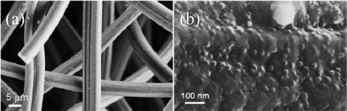 | ||
| Fig. 4 Carbon fibers: (a) FESEM image of the carbon fiber before synthesis; (b) magnified view of the carbon fiber surface. | ||
Such nucleation and growth behavior of SiC NWs is explained by their growth mechanism. For instance, the first stage of the carbothermal reduction of silicon dioxide generates gaseous silicon monoxide by reaction (1):
| SiO2(solid) + C(solid) → SiO(vapor) + CO(vapor) | (1) |
Silicon monoxide vapors are carried to the crucible cover (felt) and react with the carbon on the carbon fiber surface to form SiC crystallites by reaction (2):
| SiO(vapor) + 2C(hillock) → SiC(nanoparticles) + CO(vapor) | (2) |
In accordance with ref. 32, it can be assumed that it is the hillocks (Fig. 3b) on the carbon fibers that act as reducing agents and templates in the formation of SiC nanoparticles by reaction (2). However, reaction (2) does not ensure the growth of SiC nanowires. SiC crystallites formed by reaction (2) serve as nuclei and control the diameter of SiC NWs. Nanowires grow by reaction (3) under the conditions of CO vapor saturation:
| SiO(vapor) + 3CO(vapor) → SiC(solid) + 2CO2(vapor) | (3) |
The condition of oversaturation of CO vapors in reaction (3) is critical since under equilibrium thermodynamic conditions this reaction cannot occur at 1400 °C.6
The gaseous CO2 phase formed by reaction (3) changes to a gaseous CO phase by reaction (4):
| CO2(vapor) + C(solid) → 2CO(vapor) | (4) |
It has been shown32 that reactions (3) and (4) are related by positive feedback which finally leads to local oversaturation of the CO vapors. As it is known,33,34 in the oversaturation conditions growth occurs in the kinetic mode to form crystals and dendrites. In those conditions the (111) SiC face has the lowest surface energy. In the course of reaction (3) the silicon and carbon atoms are deposited on the SiC crystallite surface and most of them move to the face with the lowest (111) surface energy.6 In our case the existing mechanisms of formation and growth of nanowires from one-dimensional carbon nanotubes35 or metal catalysts36 with the use of templates turned out to be ineffective.
Yet, the mechanism of growth of nanowires along the [111] direction by the SiO and CO vapor reaction in the oversaturation conditions allows the explaination of most of their morphological and structural features, such as NW curvature, the presence of stacking faults and the phenomenon of NW branching.32
3.3. “Bamboo-like” nanorods
Fig. 5 shows TEM images of the “bamboo-like” nanorod. In the general case the rods consist of 3C twins. Fig. 5a shows an electron diffraction pattern of such a nanocrystalline wire along the [−110] zone axis. The marked reflections come from one of the domain systems of the 3C twins, the additional reflection system corresponds to the other domain system of the 3C twins. Rotation around the [111]-axis by 180° makes the two reflection systems overlap. The dark-field TEM image in Fig. 5b obtained from the (002) diffracted beam displays the first domain system of the 3C twins, while the dark-field TEM image from the (11−1)twin diffracted beam highlights the second domain system (Fig. 5c). More detailed analysis of the “bamboo-like” nanorods with twin domain structure is presented in Fig. 6. Fig. 6a shows the TEM bright-field image of the “bamboo-like” nanorod.![TEM images of a “bamboo-like” nanorod: (a) [−110] axis zone SAED pattern; (b) dark field TEM image in the (002) beam; (c) dark field TEM image in the (11−1) twin beam.](/image/article/2012/RA/c2ra01129h/c2ra01129h-f5.gif) | ||
| Fig. 5 TEM images of a “bamboo-like” nanorod: (a) [−110] axis zone SAED pattern; (b) dark field TEM image in the (002) beam; (c) dark field TEM image in the (11−1) twin beam. | ||
 | ||
| Fig. 6 The “bamboo-like” nanorod microstructure: (a) TEM image of the twin domain part of the “bamboo-like” rod; (b) HRTEM image of the twin domain of the wire circled in (a) with the corresponding FFT pattern inserted in the right bottom corner; (c) HRTEM image of both defect-free (1) and defect-containing (2) regions of the SiC nanorod with the corresponding FFT patterns. | ||
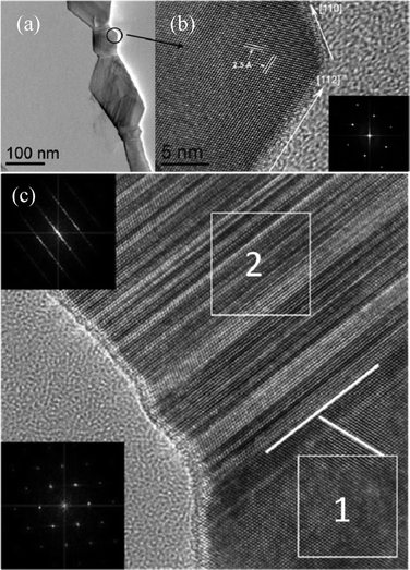
The HRTEM image of the twin domain part shows that they have a perfect 3C-structure (Fig. 6 b).
The inset presents the FFT (fast Fourier transform) pattern containing only diffraction spots for the [−110]-zone axis which confirms the absence of defects in this rod section. The crystallographic directions of the side boundaries correspond to the [112] and [110] directions, but due to the twinned structure of the “bamboo-like” nanorods, the average growth axis coincides with the [111] direction. Along with the perfect 3C domains there are segments with a high density of SFs in the “bamboo-like” nanorods. Below Fig. 6c shows the HRTEM image of the region with both defect-free (1) and defect-containing (2) segments, the white lines indicate the {111} planes. The inset in the lower left corner shows the FFT pattern of segment (1) which is identical to that presented in Fig. 6b and reflects the absence of defects in the 3C-structure of the segment. The FFT pattern of the defect-containing segment (2) is shown in the upper left corner. It contains both diffraction spots and streaks which correspond to high density of SFs. The streaks in the FFT pattern are perpendicular to the {111} atomic planes of part (2) and, hence, the growth direction of the narrow defect segments coincides with the [111]-direction.
Thus, the wide segments of the “bamboo-like” nanorods are the twin domains of the 3C-structure connected by narrow segments with a high density of SFs. The average growth axis of the “bamboo-like” nanorod coincides with the crystallographic direction of the [111]-3C-structure.
3.4. Hexagonal SiC nanoprisms and nanobelts
Fig. 7a shows the bright-field TEM image of the nanorod with hexagonal prism morphology and the corresponding HRTEM image is shown in Fig. 7b (the white line marks the close-packed {111} planes, the arrow indicates the normal direction to the {111} planes). From the HRTEM image it can be seen that the {111} planes are perpendicular to the rod growth axis and, hence, the nanorod growth direction corresponds to the [111] direction. The FFT pattern contains diffraction spots corresponding to 3C-structure as well as streaks perpendicular to the close-packed layers. As was mentioned above, the presence of such streaks points to high SF density, i.e. the absence of long-range order in the close-packed layer. Fig. 7d shows a magnified image of the framed region shown in Fig. 7b. Analysis of the sequence of the close-packed planes reveals a 3C sequence with a high density of SFs. For comparison, Fig. 7c presents an example of a perfect ABC sequence for the 3C-polytype.![The hexagonal prism SiC nanorod: (a) low magnification HRTEM image of a “smooth” SiC rod with a [111] growth direction; (b) HRTEM image of a wire showing high density or SFs; (d) magnification of the framed area shown in (b); (c) an example of a perfect 3C sequence.](/image/article/2012/RA/c2ra01129h/c2ra01129h-f7.gif) | ||
| Fig. 7 The hexagonal prism SiC nanorod: (a) low magnification HRTEM image of a “smooth” SiC rod with a [111] growth direction; (b) HRTEM image of a wire showing high density or SFs; (d) magnification of the framed area shown in (b); (c) an example of a perfect 3C sequence. | ||
Fig. 8 presents a HRTEM image of the nanobelts (white lines denote {111} planes) containing a defect-free region. The corresponding FFT pattern contains the diffraction pattern typical of the 3C twins, [−110] zone axis. Considering the above “bamboo-like” wires, it has been shown (see Fig. 6b) that the side boundaries of the defect-free 3C twin domains are directed along [110] and [112], respectively. Analysis of the HRTEM image shows that the side boundary of the bottom twin domain has a [110] direction and that of the upper domain a [112] direction, respectively, but the average growth axis of the nanobelt coincides with the [112] direction which indicates that domains with the [112] side boundary direction are dominant. Thus, the SiC nanobelts exhibit a relatively low density of SFs due to the presence of the defect-free 3C twin domains that determine the orientation of the close-packed planes and, as a result, the average belt axis coincides with the [110] or [112] directions of the 3C-structure.
 | ||
| Fig. 8 Nanobelts with a low density of SFs: HRTEM image of a defect-free nanobelt segment and the corresponding FFT pattern is inserted in the top left corner. | ||
Fig. 9 shows TEM images of another type of SiC nanobelt. Fig. 9a and b present the dark-field TEM image of the nanobelt from the (002) diffraction beam and the corresponding SAED pattern. From the SAED pattern it is seen that the growth direction of the nanobelt coincides with the [331] crystallographic direction for the 3C-structure. The presence of streaks along the [111] direction in the electron diffraction pattern points to a high density of SFs which is also confirmed by the pronounced striped structure of the nanobelt (Fig. 9a). Fig. 9c and d present the TEM image of the nanobelt and the corresponding SAED pattern indicating the [113] growth direction for this nanobelt and the presence of a high density of SFs. Common to these two cases are the extra diffraction spots (indicated by the arrows) in the SAED patterns (Fig. 9b and d) related to the hexagonal polytypes. The extra reflection intensity exceeds the intensity of the 3C-reflections, which suggests a prevalent hexagonal polytype content in these nanobelts.
![Nanobelts with a high density of SFs: (a) dark-field image of a NW with a [331] growth axis obtained in a (002) beam and the corresponding SAED pattern with a [−110] zone axis (b); (c) a dark field image of a NW with a [113] growth axis obtained in (002) beam and the corresponding SAED pattern with a [−110] zone axis (d) (arrows in the electron diffraction pattern denote the reflections of the hexagonal polytypes); (e) HRTEM image of a SiC nanobelt segment with the corresponding FFT pattern inserted in the top left corner; (f) a magnified HRTEM image of the framed area shown in (e) (the inset marked by the dashed line is a model of 2H-structure).](/image/article/2012/RA/c2ra01129h/c2ra01129h-f9.gif) | ||
| Fig. 9 Nanobelts with a high density of SFs: (a) dark-field image of a NW with a [331] growth axis obtained in a (002) beam and the corresponding SAED pattern with a [−110] zone axis (b); (c) a dark field image of a NW with a [113] growth axis obtained in (002) beam and the corresponding SAED pattern with a [−110] zone axis (d) (arrows in the electron diffraction pattern denote the reflections of the hexagonal polytypes); (e) HRTEM image of a SiC nanobelt segment with the corresponding FFT pattern inserted in the top left corner; (f) a magnified HRTEM image of the framed area shown in (e) (the inset marked by the dashed line is a model of 2H-structure). | ||
Fig. 9e shows the HRTEM image of the nanobelt with the [331] growth direction axis. In the upper left corner the corresponding FFT pattern contains diffraction spots related to the hexagonal structure. Fig. 9f presents the magnified HRTEM image of the region framed in Fig. 9e. Analysis of the sequence of the close-packed layers revealed that the sequence can be attributed to the 2H-structure with SFs. For comparison, the model of the 2H-structure is shown in the frame marked by the dashed line. It is seen that the experimental and model patterns are in full agreement with one another.
Therefore, nanobelts with a high density of SFs grow along the [113] and [331] crystallographic directions of the cubic system. It should be noted that these nanobelts contain 3C as well as 2H polytypes with a dominant content of the latter. Fig. 10a–c show the bright- and dark-field TEM images and the SAED pattern for the NW exhibiting the change in growth direction from [111] to [331]. The NW segment with the [111] growth direction has hexagonal prism morphology, an example of the cross-section of such a NW type is shown in Fig. 2b. The extensionality of the segment is indicated by the thickness contour covering the middle of the wire and is seen as a dark line on the bright-field image (Fig. 10a). The segment with the [331] growth direction has nanobelt morphology. It has been shown that the nanobelt is a rectangle with a side ratio of about 10 (Fig. 2e). The small thickness of the nanobelts can be explained by the fact that the formation of high-index side facets leads to a significant increase of plane surface energy which, as it is known,37 is minimal for {111}-type facets. The increase of specific surface energy is compensated by the reduction of the side facets surface area. It can be assumed that upon transformation from the hexagonal prism to the thin plate the cross-section area of the nanowire does not change much.
![SiC wire with a change of growth direction: (a) and (b) bright and dark field images of the NW with a changed growth axis and the corresponding SAED pattern with [−110] zone axis (c).](/image/article/2012/RA/c2ra01129h/c2ra01129h-f10.gif) | ||
| Fig. 10 SiC wire with a change of growth direction: (a) and (b) bright and dark field images of the NW with a changed growth axis and the corresponding SAED pattern with [−110] zone axis (c). | ||
3.5. Formation mechanism of various types of nanowires
The structure of all the observed SiC NWs is distinguished by the presence of SFs and twins. Frequent observations of SFs in SiC NWs can be attributed to two factors: the low energy of SF formation (34 erg cm−238) and the lower energy of the SF SiC 3C-polytype lattice as compared to that of the SF-free lattice.39,40 The presence of twins in the NWs can be accounted for by the polarity of the SiC structure.17 The energy of the Si (111) facet differs from that of the C (111) facet. Although the energy difference is assumed to be small, it will produce stress and bending in the nanorods resulting from the surface tension. Introduction of twins compensates for the difference in the surface energy caused by {111} surface polarity.
The most common morphological type of SiC NW is a hexagonal prism with the [111] growth axis. The density of SFs and twins throughout the NW length depends on the kinetic growth conditions. As was mentioned above, the hexagonal prisms nucleate and grow on the SiC crystallites with the [111] preferential growth direction and a high density of SFs and microtwins. The cross section of the crystallites gradually reduces and at some critical size the SiC nanowire starts to grow further. Generally such a kind of growth behavior of the nanowires is described by a screw dislocation growth mechanism.41
The hexagonal prism can be occasionally observed to transform to a rectangular nanobelt with a changed in the growth direction. In the case where SiC nanobelts exhibit a relatively low SF density, which is due to the presence of a certain type of defect-free 3C-structure twin domain, the mean direction of the wire axis coincides with either the [110] or [112] direction of the 3C-structure. Nanobelts with a high SF density grow in directions coinciding with the [113] and [331] directions of the cubic system. Such nanobelts contain both 3C and 2H polytypes, the latter predominating. The transformation of the wire morphology is related to the change of the growth kinetics, its reasons, however, are not completely understood. Since the formation of such high index side facets as {112}, {113} and {331} involves a considerable increase in the surface energy of the growth plane, it can be assumed that the change of the NW geometry into a high aspect ratio rectangular belt low-indexed [110] wide facet and narrow high-indexed facets takes place to avoid the increase in the surface energy.
The “bamboo-like” nanorods demonstrate randomly alternating wide and narrow regions. HRTEM analysis of this structure revealed that wide regions have a defect-free 3C-SiC lattice. The narrow regions are filled with SFs. The irregularity of the region alternation points to the intermittent nature of the growth conditions. This holds for supersaturation as the temperature throughout the whole process remained constant. As the NWs grow in the supersaturated conditions in reaction (3), it would be logical to assume that the growth of the wide regions resulted from moderate supersaturation while the growth of the narrow regions occurred upon high supersaturation. The latter brought about a considerable structure imperfection.
3.6. SiC NWs with core (SiC)–shell (SiO2) structure
Many papers report SiC NWs with a core (SiC)–shell (SiO2) structure.6 The electron-physical properties of such NWs are substantially different from “bare” analogs.2 Here we report on the production of NWs with a core–shell structure by the annealing of as-prepared “bare” SiC NWs in air at 850 °C for 4 h. Fig. 11a shows the bright-field TEM image of the obtained NW exhibiting a weak contrast shell which is assumed to belong to the amorphous SiO2 layer. The inner part has a striped structure corresponding to the SiC 3C-structure with a high density of SFs. Fig. 11b and c demonstrate the EDX mapping of the distribution of silicon (green) and oxygen (red) (carbon was not analyzed due to the parasitic emission from the carbon substrate) in the annealed and as-prepared NW samples, respectively. From Fig. 11b it is seen that the outer layer of the annealed wire contains more oxygen than its middle part while the inner layer is mainly composed of silicon. This is further proof of the formation of an outer amorphous SiO2 layer (shell) around the SiC wire surface. For comparison, Fig. 11c presents the result of EDX mapping of the as-prepared “bare” SiC NW which shows that the NW contains mostly silicon with minor fractions of oxygen.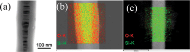 | ||
| Fig. 11 (a) Bright-field TEM image of the annealed wire with core (SiC)–shell (SiO2) structure; (b) EDX mapping of the annealed SiC wire according to the emission line and (c) EDX mapping of the initial “bare” SiC wire according to the emission line. | ||
Conclusions
The growth process of SiC NWs can be presented in the following way: the hillocks (Fig. 4b) on the carbon fibers act as reducing agents and templates in the formation of SiC nanoparticles, at the next stage SiC crystallites grow, which give rise to the growth of SiC nanorods and nanobelts. It has been noted that the growth of crystallites with a high density of SFs results in nanorod growth. The nanobelts start growing on the (111) facets of relatively perfect crystallites. Some of the nanorods have a nonuniform structure, namely, hexagonal prisms with a high density of SFs alternating with defect-free 3C twin domains, thus forming “bamboo-like” nanorods. The nanobelts can be classified into two groups: I-[112], [110] and II-[113], [331]-grown nanobelts. The type-I nanobelts have a relatively low density of SFs and contain defect-free 3C nanodomains. The orientation of the domain boundaries determines the orientation of the average belt axis. The type-II nanobelts have a high density of SFs and contain alternating sequences of small fractions of 3C and hexagonal structures. As a result, an average growth axis along the [113] or [331] directions of the 3C structure is formed.The annealing of NWs at 850 °C for 4 h in air leads to the formation of a core (SiC)–shell (SiO2) structure. The diversity of SiC NW morphology opens up a lot of opportunities for the investigation of the influence of the nanowire structure on the electrophysical, catalytic and sensory properties of nanowires.
Acknowledgements
The work was financially supported by the Program of the Russian Academy of Sciences “Physics of New Materials and Structures.”References
- C. E. Weitzel, J. W. Palmour, C. H. Carter, K. Jr. Moore, K. J. Nordquist, S. Allen, C. Thero and M. Bhatnagar, IEEE Trans. Electron Devices, 1996, 43, 1732–1741 CrossRef CAS.
- W. Zhou, L. Yan, Y. Wang and Y. Zhang, Appl. Phys. Lett., 2006, 89, 013105 CrossRef.
- K. Rogdakis, S. Y. Lee, M. Bescond, S. K. Lee, E. Bano and K. Zekentes, IEEE Trans. Electron Devices, 2008, 55, 1970–1976 CrossRef CAS.
- T. Seeger, P. K. Redlich and M. Rühle, Adv. Mater., 2000, 12, 279–282 CrossRef CAS.
- H. J. Dai, E. W. Wong, Y. Z. Lu, S. S. Fan and C. M. Lieber, Nature, 1995, 375, 769–772 CrossRef CAS.
- X. Luo, W. Ma, Y. Zhou, D. Liu, B. Yang and Y. Dai, Nanoscale Res. Lett., 2010, 5, 252–256 CrossRef CAS.
- S. Dhage, H. C. Lee, M. S. Hassan, M. S. Akhtar, C. Y. Kim, J. M. Sohn, K. J. Kim, H. S. Shin and O. B. Yang, Mater. Lett., 2009, 63, 174–176 CrossRef CAS.
- W. S. Shi, Y. F. Zheng, H. Y. Peng, N. Wang, C. S. Lee and S. T. Lee, J. Am. Ceram. Soc., 2000, 83, 3228–3230 CrossRef CAS.
- Y. W. Ryu and K. J. Yong, J. Vac. Sci. Technol., B, 2005, 23, 2069–2072 CAS.
- C. C. Tang, Y. Bando, T. Sato and K. Kurashima, Appl. Phys. Lett., 2002, 80, 4641 CrossRef CAS.
- Z. S. Wu, S. Z. Deng, N. S. Xu, J. Chen, J. Zhou and J. Chen, Appl. Phys. Lett., 2002, 80, 3829 CrossRef CAS.
- K. Zekentes and K. Rogdakis, J. Phys. D: Appl. Phys., 2011, 44, 133001 CrossRef.
- P. G. Neudeck, J. Electron. Mater., 1995, 24, 283–288 CrossRef CAS.
- H. K. Seong, H. J. Choi, S. K. Lee, J. Lee and D. Choi, Appl. Phys. Lett., 2004, 85, 1256 CrossRef CAS.
- T. D. Corrigan, D. M. Gruen, A. R. Krauss, P. Zapol and R. P. Chang, Diamond Relat. Mater., 2002, 11, 43–48 CrossRef CAS.
- A. W. Weimer, K. J. Nilsen, G. A. Cochran and R. P. Roach, AIChE J., 1993, 39, 493–503 CrossRef CAS.
- D. H. Wang, D. Xu, Q. Wang, Y. J. Hao, G. Q. Jin, X. Y. Guo and K. N. Tu, Nanotechnology, 2008, 19, 215602 CrossRef.
- D. Zhang, A. Alkhateeb, H. Han, H. Mahmood and D. N. McIlroy, Nano Lett., 2003, 3, 983–987 CrossRef CAS.
- Z. Li, W. Gao, A. Meng, Z. Geng and L. Gao, J. Phys. Chem. C, 2009, 113, 91–96 CAS.
- Z. Xie, D. Tao and J. Wang, J. Nanosci. Nanotechnol., 2007, 7, 647–652 CrossRef CAS.
- H. J. Li, Z. J. Li, A. L. Meng, K. Z. Li, X. N. Zhang and Y. P. Xu, J. Alloys Compd., 2003, 352, 279–282 CrossRef CAS.
- W. M. Zhou, B. Yang, Z. X. Yang, F. Zhu, L. J. Yan and Y. F. Zhang, Appl. Surf. Sci., 2006, 252, 5143–5148 CrossRef CAS.
- C. C. Tang, Y. Bando, T. Sato, K. Kurashima, X. X. Ding, Z. W. Gan and S. R. Qi, Appl. Phys. Lett., 2002, 80, 4641 CrossRef CAS.
- Z. L. Wang, Z. R. Dai, R. P. Gao, Z. G. Bai and J. L. Gole, Appl. Phys. Lett., 2000, 77, 3349 CrossRef CAS.
- R. B. Wu, L. L. Wu, G. Y. Yang, Y. Pan, J. J. Chen, R. Zhai and J. Lin, J. Phys. D: Appl. Phys., 2007, 40, 3697–3701 CrossRef CAS.
- Weimin Zhou, Xuan Liu and Yafei Zhang, Appl. Phys. Lett., 2006, 89, 223124 CrossRef.
- S. Dhage, H. C. Lee, M. S. Hassan, M. S. Akhtar, C. Y. Kim, J. M. Sohn and K. Ju, Mater. Lett., 2009, 63, 174–176 CrossRef CAS.
- G. W. Meng, L.D. Zhang, C. M. Mo, S. Y. Zhang, Y. Qin, S. P. Feng and H. J. Li, J. Mater. Res., 1998, 13, 2533–2538 CrossRef CAS.
- W. Stober, A. Fink and E. Bohn, J. Colloid Interface Sci., 1968, 26, 62–69 CrossRef.
- I. I. Bardyshe, A. D. Mokrushin, A. A. Pribylov, E. N. Samarov, V. M. Masalov, I. A. Karpov and G. A. Emel'chenko, Colloid J., 2006, 68, 20–25 CrossRef.
- C. Wu, X. Liao and J. Chen, Nanotechnology, 2010, 21, 405303 CrossRef.
- Y. H. Gao, Y. Bando, K. Kurashima and T. Sato, J. Mater. Sci., 2002, 37, 2023–2029 CrossRef CAS.
- A. A. Chernov, Modern crystallography III. Crystal Growth, Springer Ser. Solid-State Sci., Springer, Berlin, Heidelberg, 1984, vol. 36 Search PubMed.
- B. R. Pamplin, Crystal Growth, Pergamon Press, 2nd edn, 1980 Search PubMed.
- W. Han, Sh. Fan, Q. Li, W. Liang, B. Gu and D. Yu, Chem. Phys. Lett., 1997, 265, 374–378 CrossRef CAS.
- R. S. Wagner and W. G. Ellis, Appl. Phys. Lett., 1964, 4, 89–90 CrossRef CAS.
- H. W. Shim, J. Zhang and H. Huang, J. Appl. Phys., 2008, 104, 063511 CrossRef.
- X. G. Ning and H. Q. Ye, J. Phys.: Condens. Matter, 1990, 2, 10223 CrossRef CAS.
- L. Wang, H. Wada and L. F. Allard, J. Mater. Res., 1992, 7, 148–62 CrossRef CAS.
- C. Cheng, R. J. Needs and V. Heine, J. Phys. C: Solid State Phys., 1988, 21, 1049 CrossRef CAS.
- Jianjun Chen, Yi Pan and Renbing Wu, Phys. E., 2010, 42, 2335–2340 CrossRef CAS.
| This journal is © The Royal Society of Chemistry 2012 |