Fabrication of highly ordered multi-segment line pattern over a large-area†
Jisun
Lee
,
Su Kyoung
Lee
,
Jin-Mi
Jung
,
Youn Kyoung
Baek
and
Hee-Tae
Jung
*
Department of Chemical and Biomolecular Engineering (BK21), Korea Advanced Institute of Technology, Daejeon, Korea. E-mail: Heetae@Kaist.ac.kr; Fax: +82 42 350 3910; Tel: +82 42 350 3971
First published on 12th January 2012
Abstract
We report on the fabrication of well-aligned multi-segment line patterns over large areas featuring dimensional and compositional exquisite tunability using a combination of photolithography and soft-lithography techniques. We show that thus this new top-down approach has great advantages and that it is beneficial by increasing the control of the multi-segment line width and pattern feature dimensions ranging from microns to a few hundred nanometres. Various combinations of multi-segment materials with full control over the periodic alignment, which include Au–Ni, Au–Cu and Au–Ag, were prepared by simply changing the metals evaporated before the lift-off process. Au–Ni multi-segment metal line patterns showed a linear current–voltage response, identical with that of a line pattern from a single material. Thus, one can take advantage of the simple electrical properties of the 1-dimensional nanostructure. Our approach provides great potential in practical fabrication of well-integrated multi-metal component devices for electrical and optical detection.
1. Introduction
The development of one dimensional (1D) structures has attracted considerable attention in various applications including nanoscale electronics and electronic sensing devices due to their directivity, large surface area and intrinsic quantum confinement effects.1–3 Among 1D nanostructures, a multi-segment nanowire, consisting of two or more kinds of material arranged alternately in the longitudinal direction, can be fabricated for specific end-use applications depending on the design constraints. By the simultaneous use of unique chemical, optical and electrical properties of each nanowire component, one can obtain a versatile circuit element for devices such as sensors,4–6 wave-guides7,8 and micro-electromechanical system (MEMS).9,10 The fabrication of multi-segment nanostructures has been generally accomplished by directed crystal growth from anisotropically shaped nanoparticle11,12 or the electrochemical deposition with an AAO (anodic aluminium oxide) template.13,14 The crystal growth method produces a robust interface between two materials but is limited by material availability and the control of growth conditions. Template-assisted electrochemical deposition is the most popular method to fabricate the multi-segment nanowires and can incorporate a wide range of component couplings such as metal–metal,15 metal–semiconductor16 and metal–organic.17,18 The templates provide good directivity and productivity due to high pore density; however, it is difficult to control the feature size and segment length. The transfer of the multi-segment nanowires to a desired substrate with a structural arrangement is also problematic. Therefore, a facile fabrication method to control both the segment component and arrangement of nanowires on a substrate is essential to realizing multi-segment nanowire properties, as well as the fabrication of elements approaching wafer-scale integrated devices.Here we report a new method to fabricate various multiple segment line patterns through soft lithography19–25 combined with a conventional photolithography technique. Our approach confers effectiveness to control the direction and location of multi-segment nanowires over a large area (5 mm × 5 mm) with high flexibility to generate different dimensions of line patterns and composition of materials. The high reproducibility of fine features by our method is expected to contribute to a development of novel devices integrated with multi-segment nanowires in the electrical, biological and optical sensing areas.4–6
2. Experimental section
A schematic process for fabricating the multi-segment line patterns by the combined lithographic process is shown in Fig. 1. Our patterning strategy starts by taking advantage of photolithography, which is the most efficient method to generate microscale patterns. First, gold (Au) was deposited on a substrate (Si wafer or glass) using an e-beam evaporator with a chrome (Cr) adhesion layer (∼3 nm). Next, the AZ® 5214 PR (Clariant Co. Ltd.) layer was spin-coated on the Au surface. The approximately 1 μm layer thickness was exposed to a 365 nm UV lamp using a 5 μm linewidth mask; The photoresist (PR) pattern was then treated with AZ® developer solution (Clariant Co. Ltd.). With the PR line pattern, a similar arrangement of Au lines was produced by Ar+ ion milling (20 sccm, 7.0 × 10⁻⁴ Torr, 500 mV). A second metal (Ni) was subsequently deposited on the patterned area so as to fill the spaces between the Au lines.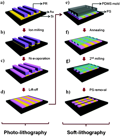 | ||
| Fig. 1 Schematic diagram of the fabrication process for a multi-segment line pattern. Photoresist (PR) patterns were formed by photolithography (a). The exposed surface of metal I is etched by an ion-milling process (b). After metal II is evaporated (c), the PR is removed by a lift-off process (d) resulting in the metal ribbon pattern shown. PS solution is spin-coated and then the line patterned PDMS mold is placed on the metal ribbon surface with the desired direction (e). After annealing, the PS etch mask is fabricated (f) and further etched by ion-milling (g). Finally residual PS was removed by reactive ion etching (RIE) (h). | ||
After the lift-off process to remove all PR residue by sonication with an organic solvent, a metal layer with aligned Au and Ni metal ribbons was obtained. The line width of the metal ribbons can be varied by using different photomasks and in this example, the linewidth and spacing was 5 μm.
In the second part of the procedure, soft lithography was implemented to generate the multi-segment line pattern and to precisely control its line width. We have previously demonstrated that the fabrication of a variety of nano-sized features can be achieved from a single master by controlling the polymer replica shape formed by a polydimethylsiloxane (PDMS) soft mold.20,23,24,26–28 First, polystyrene (PS, molecular weight ∼20 kg mol−1) was spin-coated to form a thin polymeric layer on the metal ribbon surface; a PDMS mold with the desired topographical line features was placed on the top surface oriented in a perpendicular direction relative to the alignment of the metal ribbons. By annealing the PS above its glass transition temperature (∼135 °C) for 90 min, capillary forces cause the polymer fluid to form lines along the channels of the PDMS mold on the prepared substrate. Next, reactive ion etching (RIE) with a gas mixture of O2 (40 sccm) and CF4 (60 sccm) plasma is used to remove residual polymer, thus preserving line features. The resultant PS pattern acts like an etch-mask for the metal substrate in order to generate the final line pattern of Au–Ni during a second ion-milling process. Lastly, the etching mask of the PS layer on the top surface was removed by RIE (100 sccm O2; 80 W; 0.3 Torr) and washing with methylene chloride several times.
3. Results and discussion
As shown in Fig. 2, Au–Ni multi-segment metal line patterns were successfully fabricated from a 5 μm line patterned mask (with 5 μm spacing) for the photolithography, and a 500 nm line patterned mold for the soft lithography. The two metals can be recognized by the contrast in the SEM image; note that the brighter part of the line pattern indicates gold, which is more conductive than Ni. The images also confirm that each component has a conformal edge, thus producing a clear boundary between the two metals without a gap. Even though there is line edge roughness induced by the lift-off and ion-milling process, it brings negligible roughness to the overall features, merely an effect on the contact between each segment and also the quality of the entire line pattern. | ||
| Fig. 2 Scanning electron microscopy (SEM) images of (a) Au–Ni multi-segment line pattern and (b) the Au–Ni junction. (c) Energy dispersive spectroscopy (EDS) peaks of Au, Ni and Si wafer. SEM (Sirion FE-SEM, FEI) images and EDS peaks were obtained by collecting the secondary electrons produced by irradiating the sample with an incident electron beam of energy 10 kV. | ||
Other multi-segment patterns were produced by varying the metals evaporated before the lift-off process, using Au as the bottom metal (Fig. 1a). Ni, Cu or Ag was deposited on the PR patterned substrate via e-beam evaporation after the first milling process (Fig. 1c). Platinum (Pt) is a passivation layer evaporated onto Cu to prevent Cu oxidation during RIE. In addition to the Au–Ni line patterns shown in Fig. 2, other types of multi-segment line patterns were produced including Au–Cu (Fig. 3a) and Au–Ag (Fig. 3b). Each of these compositions was confirmed by elemental analysis using EDS. The corresponding peak intensities were relatively weaker than Si because the metal layer thickness was very thin (∼50 nm) with respect to the substrate. However, the signal to noise ratio further verifies the existence of each metal. In the second metal evaporation step, we needed to control the metal thickness very carefully due to the selective removal of material. In other words, if two metals having different etch rates are deposited with the same thickness, the faster etchable metal segment disappears easily while the other metal is maintained during the ion-milling process.
 | ||
| Fig. 3 Multi-segment line patterns with different compositions. (a) SEM image of an Au–Cu line pattern on a quartz substrate; (b) EDS peaks corresponding to each material; (c) SEM image of an Au–Ag line pattern on a Si substrate; (d) corresponding EDS data. | ||
Therefore, the thickness of the secondary metal should be controlled with respect to the etch rate of the first metal evaporated. For example, to make the Au–Ni line pattern, the ion-milling etch rate ratio between Au and Ni is 3![[thin space (1/6-em)]](https://www.rsc.org/images/entities/char_2009.gif) :1(18 nm min−1:6 nm min−1). Therefore Ni should be evaporated with one third the thickness of Au.
:1(18 nm min−1:6 nm min−1). Therefore Ni should be evaporated with one third the thickness of Au.
We further demonstrate that the width of the final multi-segment line pattern can be controlled. In soft lithography, various factors are related to the final dimension of the line pattern.27–32 Here we chose to vary the feature size of the line pattern and the thickness of the polymer film.
Two different molds, with 500 nm and 1000 nm lines and spacing, were used; the PS thickness was varied between 50 nm and 120 nm. Fig. 4a and 4b show that when the polymer film is thick enough, the dimensions of the metal stripes are matched with that of the PDMS mold. In contrast, Fig. 4c shows 200 nm width lines from the same mold used to produce the pattern shown in Fig. 4b because the PS film was thinner than the previous case and the PS fluid separated into two meniscuses due to capillary forces.33
 | ||
| Fig. 4 SEM images of the Au–Cu line pattern with different feature sizes. Line width and spacing: (a) 500 nm, (b) 1 μm, (c) 200 nm patterns. (b) and (c) were generated from the same PDMS mold, however the dimensions of the line width and spacing varied depending on the PS layer thickness. | ||
To investigate the feasibility of practical electrical device fabrication, we examined the electrical properties of the multi-segment line pattern. A pair of gold electrodes (Cr/Au = 10/100 nm) was made at both ends of the line pattern with a 3 mm separation. The SEM images shown in Fig. 5 indicate three types of line patterns: (a) Au, (b) Ni and (c) Au–Ni. The multi-segment line patterns were prepared with 500 nm width lines.
 | ||
| Fig. 5 SEM images of (a) Au, (b) Ni and (c) Au–Ni line patterns with 500 nm line width. (d) I–V curve of line patterns (a), (b) and (c). Electrical measurements were accomplished by a parametric analyzer (4200-SCS, Keithley). | ||
Linear current–voltage (I–V) plots corresponding to all three patterns were measured (Fig. 5d) under the voltage sweep conditions from −1 to 1 V. The segmented line pattern (c) shows similar I–V behavior as that produced from the Au line pattern and Ni lines, indicating a good ohmic contact. The slope of the I–V curve is simply a measure of the inverse resistance or conductance as stated by Ohm's law. The data presented in Fig. 5d clearly shows that the conductance of the multi-segment line pattern falls between that of the single metal patterns. The obvious implication is that pattern (c) has tunable resistance by adjustment of the ratio of the constituent metals.
4. Conclusions
In summary, we have demonstrated how to produce a highly reproducible multi-segment line array on a substrate through the combination of photolithography and soft lithography. During the photolithography process, we efficiently produced a substrate consisting of two different metal lines stacked alternatively. Then, using soft lithography in the perpendicular direction to the substrate line, we produced the desired multi-segment line pattern. Our method is capable of fabricating various combinations of metals into a multi-segment line pattern. Here we showed multi-segment patterns consisting of Au–Ni, Au–Ag or Au–Cu, and other combinations of multi-segment materials can be prepared, provided the materials are removable through dry etching. Also, we controlled the line width of the pattern by varying the soft lithography conditions such as the PDMS mold and PS film thickness to produce a range of line widths from 1 μm to 200 nm. By varying the ratio of metals, we can systematically adjust the conductance of the multi-segment line pattern. We expect that multi-segment line patterns will find useful applications for various micro/nano electronic devices including resistors, capacitors and electrical/optical biosensors.Acknowledgements
This work was supported by the National Research Laboratory Program (R0A-2007-000-20037-0, KOSEF) and the World Class University Program (R32-2008-000-10142-0, KOSEF) and National Research Foundation of Korea (NRF) funded by the Ministry of Education, Science and Technology (No. 2009-008338). SEM experiments were carried out at NNFC.References
- Y. Xia, P. Yang, Y. Sun, Y. Wu, B. Mayers, B. Gates, Y. Yin, F. Kim and H. Yan, Adv. Mater., 2003, 15, 353 CrossRef CAS.
- L. A. Bauer, N. S. Birenbaum and G. J. Meyer, J. Mater. Chem., 2004, 14, 517 RSC.
- A. A. Argun and J. R. Reynolds, J. Mater. Chem., 2005, 15, 1793 RSC.
- R. M. Hernández, L. Richter, S. Semancik, S. Stranick and T. E. Mallouk, Chem. Mater., 2004, 16, 3431 CrossRef.
- H.-J. Chung, H. H Jung, Y.-S. Cho, S. Lee, J.-H. Ha, J. H. Choi and Y. Kuk, Appl. Phys. Lett., 2005, 86, 213113 CrossRef.
- U. S. Ramelow, J. H. Ma and R. Darbeau, Mater. Res. Innovations, 2001, 5, 40 CrossRef CAS.
- S. A. Maier, P. G. Kik, H. A. Atwater, S. Meltzer, E. Harel, B. E. Koel and A. A. G. Requicha, Nat. Mater., 2003, 2, 229 CrossRef CAS.
- J. J. Mock, S. J. Oldenburg, D. R. Smith, D. A. Schultz and S. Schultz, Nano Lett., 2002, 2, 465 CrossRef CAS.
- N. I. Kovtyukhova, B. K. Kelly and T. E. Mallouk, J. Am. Chem. Soc., 2004, 126, 12738 CrossRef CAS.
- S. Liu, J. B.-H. Tok and Z. Bao, Nano Lett., 2005, 5, 1071 CrossRef CAS.
- D. Seo, C. I. Yoo, J. Jung and H. Song, J. Am. Chem. Soc., 2008, 130, 2940 CrossRef CAS.
- L. Li, T. Zhai, H. Zeng, X. Fang, Y. Bando and D. Golberg, J. Mater. Chem., 2011, 21, 40 RSC.
- S. J. Hurst, E. K. Payne, L. Qin and C. A. Mirkin, Angew. Chem., Int. Ed., 2006, 45, 2672 CrossRef CAS.
- X. Wang and C. S. Ozkan, Nano Lett., 2008, 8, 398 CrossRef CAS.
- J. J. Mock, S. J. Oldenburg, D. R. Smith, D. A. Schultz and S. Schultz, Nano Lett., 2002, 2, 465 CrossRef CAS.
- N. I. Kovtyukhova, B. K. Kelley and T. E. Mallouk, J. Am. Chem. Soc., 2004, 126, 12738 CrossRef CAS.
- S. Park, J.-H. Lim, S.-W. Chung and C. A. Mirkin, Science, 2004, 303, 348 CrossRef CAS.
- M. E. Ibele, R. Liu, K. Beiswenger and A. Sen, J. Mater. Chem., 2011, 21, 14410–14413 RSC.
- G. Whiteside, Angew. Chem., Int. Ed., 1998, 37, 550 CrossRef.
- K. Y. Suh, Adv. Mater., 2001, 13, 1386 CrossRef CAS.
- H.-H. Park, D.-G. Choi, X. Zhang, S. Jeon, S.-J. Park, S.-W. Lee, S. Kim, K.-D. Kim, J.-H. Choi, J. Lee, D. K. Yun, K. J. Lee, H.-H. Park, R. H. Hill and J.-H. Jeong, J. Mater. Chem., 2010, 20, 1921 RSC.
- S.-J. Jeong and S. O. Kim, J. Mater. Chem., 2011, 21, 5856 RSC.
- H.-J. Jeon, Y.-K. Baek, S. B. Yang, S.-K. Lee, J.-M. Jung and H.-T. Jung, J. Mater. Chem., 2011, 21, 14285–14290 RSC.
- T. Gang, O. Yildirim, S. Kinge, X. Duan, D. N. Reinhoudt, D. H. A. Blank, G. Rijnders, W. G. van der Wiel and J. Huskens, J. Mater. Chem., 2011, 21, 14800–14806 RSC.
- J. J. Richardson, D. Estrada, S. P. DenBaars, C. J. Hawker and L. M. Campos, J. Mater. Chem., 2011, 21, 14417–14419 RSC.
- J.-M. Jung, F. Stellacci and H.-T. Jung, Adv. Mater., 2007, 19, 4392 CrossRef CAS.
- S.-K. Lee, J.-M. Jung, J. Lee and H.-T. Jung, Langmuir, 2010, 26, 14359 CrossRef CAS.
- H. Schmid and B. Michel, Macromolecules, 2000, 33, 3042 CrossRef CAS.
- S. Kim, J. Appl. Phys., 2006, 99, 08G310 CrossRef.
- S. Kim, Langmuir, 2006, 22, 7109 CrossRef CAS.
- H.-L. Zhang, Nano Lett., 2004, 4, 1513 CrossRef CAS.
- C. M. Bruinink, Adv. Funct. Mater., 2006, 16, 1555 CrossRef CAS.
- K. Y. Suh, P. J. Yoo and H. H. Lee, Macromolecules, 2002, 35, 4414 CrossRef CAS.
Footnote |
| † Electronic supplementary information (ESI) available. See DOI: 10.1039/c2ra01120d |
| This journal is © The Royal Society of Chemistry 2012 |