Controlled synthesis and photoelectrochemical properties of highly ordered TiO2 nanorods
Sadia
Ameen†
a,
M. Shaheer
Akhtar†
b,
Young Soon
Kim
a and
Hyung Shik
Shin
*a
aEnergy Materials & Surface Science Laboratory, Solar Energy Research Center, School of Chemical Engineering, Chonbuk National University, Jeonju, 561-756, Republic of Korea. E-mail: hsshin@jbnu.ac.kr (H.S. Shin); Fax: +82-63-270-2306
bNew & Renewable Energy Material Development Center (NewREC), Chonbuk National University, Jeonbuk, 561-756, Republic of Korea
First published on 18th April 2012
Abstract
Highly ordered TiO2 nanorods (NRs) were grown directly on fluorine doped tin oxide (FTO) substrate by a single step hydrothermal synthesis at 150 °C. The morphology of TiO2 was significantly altered by changing the solvents of ethanol/deionized (DI) water as the precursor solutions. With ethanol/DI water (80![[thin space (1/6-em)]](https://www.rsc.org/images/entities/char_2009.gif) :20 v/v) as solvent, the highly ordered tetragonal TiO2 NRs were achieved on FTO substrates with the average lengths of ∼2–4 μm and diameters ∼50–70 nm respectively. While, the round headed and distorted hexagonal TiO2 NRs were formed with ethanol/DI water ratios of 50:50 v/v and 0:100 v/v as the precursor solutions respectively. The grown TiO2 NRs possessed the anatase phase with typical tetragonal crystal structures. XPS studies evidenced that the grown TiO2 NRs exhibited the O:Ti stoichiometric ratio of 2:1 with lower impurities of the carbon species. The grown TiO2 NRs thin film substrates were applied as photoanodes for efficient dye-sensitized solar cells (DSSCs). A solar-to-electricity conversion efficiency of ∼3.2% was achieved by DSSC, fabricated with highly ordered tetragonal TiO2 NRs photoanode, whereas DSSC with the distorted hexagonal TiO2 NRs photoanode showed inferior overall conversion efficiency (∼1.08%). The improved photovoltaic performance was credited to the highly ordered morphology of the TiO2 NRs, which executed the high charge collection and the transfer of electrons at the interfaces of the TiO2 NRs photoanode and the electrolyte layer.
:20 v/v) as solvent, the highly ordered tetragonal TiO2 NRs were achieved on FTO substrates with the average lengths of ∼2–4 μm and diameters ∼50–70 nm respectively. While, the round headed and distorted hexagonal TiO2 NRs were formed with ethanol/DI water ratios of 50:50 v/v and 0:100 v/v as the precursor solutions respectively. The grown TiO2 NRs possessed the anatase phase with typical tetragonal crystal structures. XPS studies evidenced that the grown TiO2 NRs exhibited the O:Ti stoichiometric ratio of 2:1 with lower impurities of the carbon species. The grown TiO2 NRs thin film substrates were applied as photoanodes for efficient dye-sensitized solar cells (DSSCs). A solar-to-electricity conversion efficiency of ∼3.2% was achieved by DSSC, fabricated with highly ordered tetragonal TiO2 NRs photoanode, whereas DSSC with the distorted hexagonal TiO2 NRs photoanode showed inferior overall conversion efficiency (∼1.08%). The improved photovoltaic performance was credited to the highly ordered morphology of the TiO2 NRs, which executed the high charge collection and the transfer of electrons at the interfaces of the TiO2 NRs photoanode and the electrolyte layer.
Introduction
Due to versatile and the exotic properties, titania (TiO2) nanomaterials are so far used in many technological applications as a photocatalyst, photovoltaic material, gas sensor, optical coating, structural ceramic, electrical circuit varistor, biocompatible material for bone implants, and spacer material for magnetic spin valve systems etc.1–9 The dimensionality of TiO2 at the nanoscale level is the crucial characteristic for determining the physiological and electrical properties. In recent years, one dimensional (1D) TiO2 nanomaterials like nanorods (NRs), nanowires (NWs) and nanotubes (NTs) display significantly larger surface areas as compared to bulk materials, which deliver unique chemical and the physical properties10 and 11 contribute towards the electrical and photoelectrochemical applications.12,13 The 1D TiO2 such as NRs and NTs have shown the reduced recombination rate for the excited electron-hole pair and display unique optical and the electric properties.14,15 Particularly, the vertically grown TiO2 NRs allow shorter and the uninterrupted electrical pathways for the photogenerated carriers and improves the charge separation and charge transport properties in many photoelectrochemical devices like dye sensitized solar cells (DSSCs).16 As compared to TiO2 nanoparticles,17,18 it is expected that the highly oriented TiO2 NRs could be the potential electrode and photocatalyst material for several photoelectrochemical applications.So far, several techniques are available for synthesizing the oriented or disoriented 1D TiO2 nanostructures on nontransparent or nonconductive substrates.19–21 The hydrothermal method is an effective, easily controllable and low cost technique for the growth of highly oriented TiO2 NRs on various substrates.22 Until now, little work has been reported for the growth of crystalline TiO2 NRs on the transparent conducting oxide (TCO) by the hydrothermal method.23 The randomly assembled and the connected dense TiO2 NR arrays were grown on the TCO substrates by the hydrothermal method.24 Recently, the direct growth of rutile TiO2 NR arrays on FTO substrates was investigated by Liu et al.,25 which demonstrated the photovoltaic properties of DSSCs. In this paper, the highly ordered TiO2 NRs are directly grown on the FTO substrate by a single step hydrothermal synthesis with ethanol/deionized (DI) water and DI water in the precursor solutions at 150 °C. The highly ordered tetragonal TiO2 NRs were obtained on FTO substrates with ethanol/DI water (80:20 v/v) as solvent, however, the round headed and distorted hexagonal TiO2 NRs were formed with ethanol/DI water ratios of 50:50 v/v and 0:100 v/v respectively. An improved solar-to-electric conversion efficiency of ∼3.2% is achieved by the highly ordered tetragonal TiO2 NRs under 100 mW cm−2 (1.5 AM).
Materials and methods
a) Synthesis of TiO2 NRs on FTO substrate
For highly ordered tetragonal TiO2 NRs, the precursor solution was obtained by dissolving 50 ml of concentrated hydrochloric acid (HCl, Daejung Chemicals, 35%) in 50 ml of a mixed solution of absolute ethanol/DI water (80:20 v/v), and the mixture was stirred at ambient conditions for 30 min. Here, the HCl was added to optimize the control of oxide precipitation and the solution stability. Thereafter, 1.5 ml titanium butoxide (Ti(OB)4, Aldrich-sigma, 98% assay) was added drop by drop into the precursor solution under constant stirring for 1 h. The pH of the reaction mixture was in the range of ∼1.5–2. The FTO (FTO glass, Hartford Glass Co., 8Ω sq−1, 80% transmittance in visible spectrum) glass substrates were degreased and cleaned sequentially by sonicating in acetone, ethanol and DI for about 30 min and were finally dried in an air. The whole reaction mixture solution was transferred into a Teflon beaker and the pieces of cleaned FTO substrates were placed in the Teflon beaker with the conducting side facing downward. The Teflon beaker was sealed into a stainless steel autoclave and maintained at 150 °C for 10 h. After completion of the reaction, the autoclave was cooled under flowing water for about 15 min. The substrates were taken out and rinsed with DI water and methanol several times and allowed to dry in ambient air. On the other hand, the round headed and distorted hexagonal TiO2 NRs were synthesized in a similar way, using 50 ml of a solution of ethanol/DI water (50:50, v/v) and (0:100, v/v) with 50 ml concentrated HCl and 1.5 ml Ti(OB)4 respectively.
b) Fabrication of aligned TiO2 NR based DSSCs
The fabrication of DSSC was performed accordingly as reported elsewhere.26 In brief, the prepared TiO2 NR thin film FTO substrates were immersed in an ethanolic solution of ruthenium(II) 535 bis-TBA dye (0.3 mM, N-719, Solaronix) for 20 h at room temperature under dark conditions. The dye adsorbed TiO2 NR thin film electrodes were rinsed with absolute ethanol and dried under a nitrogen stream at 40 °C. The platinum (Pt) deposited FTO substrates were used as a counter electrode and was placed over the dye immobilized TiO2 NR thin film electrode. The edges of the cell were sealed with a 60 μm thick Surlyn sheet (SX 1170-60, Solaronix) by hot-pressing the two electrodes at 80 °C. An electrolyte of specified composition (0.5 M LiI, 0.05 mM I2, and 0.2 M tert-butyl pyridine in acetonitrile) was introduced through the holes of the counter electrode on the dye immobilized TiO2 NR thin film photoanode and the holes were sealed with a piece of small microscopic glass and a Surlyn sheet.c) Characterization
The TiO2 NRs thin films were characterized by the field emission scanning electron microscopy (FESEM, Hitachi S-4700) and transmission electron microscopy (TEM, JEM-2010-JEOL, Japan). Crystalline structures of the TiO2 NRs thin film were studied by X-ray powder diffraction (XRD, Rigaku, Cu-Kα, λ = 1.54178 A°) in the Bragg angle ranging between 20°. The Raman spectrum (Raman microscope, Renishaw) and the UV-visible absorbance (2550 Shimadzu, Japan) were used to characterize the optical properties and the absorption spectra. X-rays Photoelectron Spectroscopy (XPS) was performed by using AXIS-NOVA CJ109, Kratos Inc., ranges 0–800 eV to investigate the bonding of TiO2. A current density (J)-voltage (V) curve was measured using a computerized digital multimeter (model 2000, Keithley) with a variable load. A 1000 W metal halide lamp was used as a light source and its light intensity was adjusted to simulate 1.5 AM at 100 mW cm−2 with a Si photo detector fitted with a Ka-5 filter as a reference, calibrated at NREL, USA. A black tape mask was placed on top of the cell during the J-V measurements. The operating temperature in the range of 20–30 °C was maintained by the small cooling fan. The incident photon-to-current conversion efficiency (IPCE) was carried out by a specially designed IPCE system for DSSC by PV measurements, Inc., USA. Before performing the IPCE measurement, the system was calibrated with a silicon photodiode, which was calibrated using the NIST-calibrated photodiode G425 as a standard. IPCE results of DSSCs were collected as a function of wavelength from 400 to 800 nm using a 75 W Xe lamp as a light source for generating monochromatic beam at a low chopping frequency.Results and discussion
Fig. 1 shows the typical surface FESEM images of the TiO2 NR thin films deposited on FTO substrates by the hydrothermal process with variations of the ethanol/DI water precursor solution. The distorted hexagonal TiO2 NRs (Fig. 1(a, b)) of average diameter ∼100–200 nm and length of ∼3.0 μm are obtained with an ethanol/DI water ratio of 0:100 v/v as the precursor solution whereas, Fig. 1(c, d) exhibits the round headed TiO2 NRs with ethanol/DI water (50:50 v/v) as the precursor solution. Sequentially, the highly ordered tetragonal TiO2 NRs have grown on the FTO substrate with the precursor solution of ethanol/DI water (80:20 v/v). The grown TiO2 NRs possess the average lengths of ∼2–4 μm and diameters of ∼50–70 nm respectively, as shown in Fig. 1(e, f). The high amount of ethanol in the precursor solution is crucial to achieve the highly ordered nanorods. Thus, it could be seen that the morphology of the TiO2 NRs changes with the solvents such as ethanol/DI water and DI water as the precursor solutions.
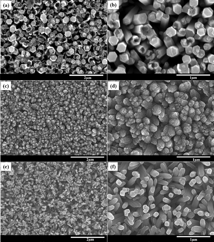 | ||
| Fig. 1 Low and high resolution FESEM images of the TiO2 NR thin films obtained with the precursor solutions of ethanol/DI water with ratios of (a, b) 0:100 v/v, (c, d) 50:50 v/v and (e, f) 80:20 v/v. | ||
Fig. 2 shows the transmission electron microscopy (TEM), high resolution (HR) TEM and the selected area electron patterns (SAED) of the grown TiO2 NR coated FTO substrate. Similar to theFESEM results, the highly ordered tetrgonal TiO2 NRs from the precursor solution of ethanol/DI water (80:20 v/v) solvent comprises the average length of ∼2–4 μm and the diameter of ∼50–70 nm, as shown in Fig. 2 (a). Each NR is made of a bundle of the densely packed nanofibers (NFs) with an average fibril's diameter of ∼5 nm. The corresponding SAED pattern (Fig. 2(b)) displays the clear phases, suggesting the high crystal quality with the single crystalline fibrils derived from TiO2 NRs along the [001] direction. However, the HRTEM image (Fig. 2(c)) shows the well-resolved lattice fringes of the grown TiO2 NRs and estimates an average interplanar distance of ∼0.35 nm between the two fringes, which reveals the typical interplanar distance of anatase TiO2.27 On the other side, the width and length of distorted hexagonal TiO2 NRs are respectively observed as ∼200 nm and ∼3.2 μm, as seen in Fig. 2 (d).
 | ||
| Fig. 2 TEM image of (a) highly ordered tetragonal TiO2 NRs, (b) SAED patterns, (c) HRTEM image and (d) TEM image of grown hexagonal distorted TiO2 NRs. | ||
Fig. 3 displays the XRD patterns of highly ordered tetragonal and distorted hexagonal TiO2 NRs grown on the FTO substrate. The grown TiO2 NRs from both precursor solutions exhibit the anatase phase with the peaks at 25.1°, 37.9°, 48.1°, 53.8° and 55.1°, which correspond to typical anatase TiO2 materials and indexes at JCPDS no. 89-4203. However, the diffraction peaks of the FTO substrate are also observed at 33.8°, 35.7° and 52.8° (JCPDS no. 88-0287). On comparison with the distorted hexagonal TiO2 NRs, the intensities of XRD diffraction peaks have minutely changed, which might indicate the high crystalline nature of the highly ordered tetragonal TiO2 NRs.
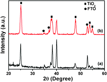 | ||
| Fig. 3 XRD patterns of (a) the distorted hexagonal TiO2 NRs and (b) the highly ordered tetragonal TiO2 NR thin film. | ||
To understand the absorption and optical properties, UV-Vis spectroscopy of the TiO2 NR thin film substrates are examined. As shown in Fig. 4, both the grown TiO2 NRs exhibit a broad absorption in the ultraviolet region (<400 nm), corresponding to the typical anatase TiO2 absorption edge in the UV region.28 Furthermore, the band gap energies are calculated as ∼3.26 eV and ∼3.21 eV for the highly ordered tetragonal and distorted hexagonal TiO2 NRs respectively, which are very close to the anatase TiO2 in bulk. The low band gap energy and the absorption intensity of the distorted hexagonal TiO2 might display the low optical properties of TiO2 materials.
 | ||
| Fig. 4 UV-Vis spectroscopy of (a) the distorted hexagonal TiO2 NRs and (b) the highly ordered tetragonal TiO2 NR thin film. | ||
Fig. 5 shows the Raman scattering spectra of the grown highly ordered tetragonal and distorted hexagonal TiO2 NRs. The grown TiO2 NRs display the Raman band in the range of 200–800 cm−1, representing the characteristic peaks of O–Ti–O in TiO2 nanomaterials.29 In both grown TiO2 NRs, the three Raman bands are observed at ∼396, ∼514.4 and ∼638.1 cm−1 in the spectrum, which corresponds to the phonon modes of the anatase phase.30,31 The Raman band at ∼ 638.1 cm−1 has been assigned to the symmetric Ti–O vibration from the Ag symmetric modes of the TiO6 octahedra,32 whereas those at ∼396 and ∼514.4 cm−1 refer to the splitting of the degenerate mode of the TiO6 octahedra in the TiO2 nanostructures.33 Importantly, the appearance of the strong and broad band peak at ∼396 cm−1 is the main peak, which indicates the formation of the TiO2 nanostructures.34 Compared to the distorted hexagonal TiO2 NRs, the high intensity Raman bands of highly ordered tetragonal TiO2 NRs might ascribe to its better optical and crystalline properties.
 | ||
| Fig. 5 Raman scattering spectroscopy of (a) the distorted hexagonal TiO2 NRs and (b) the highly ordered tetragonal TiO2 NR thin film. | ||
X-Ray photoelectron spectroscopy (XPS) has been carried out to investigate the chemical state of the elements in the grown TiO2 NRs (Fig. 6). As shown in Fig. 6(a), Ti 2p spectrum is the doublet binding energy peaks at ∼459.2 eV and ∼464.9 eV, corresponding to Ti 2p3/2 and Ti 2p1/2 respectively.35,36 The observed binding energy of Ti 2p accomplishes the +4 oxidation state of Ti, i.e., the Ti+4 state. The peak separation of ∼5.7 eV is noticed between the Ti 2p1/2 and Ti 2p 3/2 binding energies, which is in excellent agreement with the reported pure TiO2 values.37 The deconvoluted O 1s XPS spectra (Fig. 6(b)) displays four fitted peaks at ∼530.4, ∼531.3, ∼532.1, and ∼532.6 eV. The main central binding at ∼530.4 eV represents the oxygen attached to the Ti atom in the manner of Ti–O–Ti (lattice O), however, the other three O 1s peaks appear at ∼531.3 eV, 532.1 eV and 532.6 eV, ascribed to C![[double bond, length as m-dash]](https://www.rsc.org/images/entities/char_e001.gif) O, the hydroxyl group attached with Ti, and C–OH (and C–O–C) species respectively.38,39 Similarly, the C 1s XPS (Fig. 6(c)) shows the two binding energies at ∼285.4 eV and 289.1 eV, assigning the C–C and C–O species, which usually occur by the presence of impurities from the metal alkoxide precursor during the hydrothermal process.40,41 Thus, from Ti 2p and O 1s results, the grown TiO2 NRs might form in the nearly stoichiometric ratios of TiO (2:1) and contain much less impurities of the C species.
O, the hydroxyl group attached with Ti, and C–OH (and C–O–C) species respectively.38,39 Similarly, the C 1s XPS (Fig. 6(c)) shows the two binding energies at ∼285.4 eV and 289.1 eV, assigning the C–C and C–O species, which usually occur by the presence of impurities from the metal alkoxide precursor during the hydrothermal process.40,41 Thus, from Ti 2p and O 1s results, the grown TiO2 NRs might form in the nearly stoichiometric ratios of TiO (2:1) and contain much less impurities of the C species.
 | ||
| Fig. 6 Ti 2p (a), O 1s (b) and C 1s (c) XPS spectra of the grown highly ordered tetragonal TiO2 NRs. | ||
The current density–voltage (J–V) characteristics (Fig. 7(a)) have been performed to elucidate the performance of the DSSCs fabricated with the photoanodes of grown TiO2 NRs and were measured under a light intensity of 100 mW cm−2 (1.5 AM). DSSCs fabricated with the photoanode of distorted hexagonal TiO2 NRs executes a relatively low solar efficiency of ∼1.08%, with a low short circuit current (JSC) of ∼4.48 mA cm−2, open circuit voltage (VOC) ∼0.571 V and fill factor (FF) of ∼0.42. However, DSSCs fabricated with the photoanode of highly ordered tetragonal TiO2 NRs shows an appreciably improved overall conversion efficiency of ∼3.2% with a high JSC of ∼8.7 mA cm−2, VOC of ∼0.67 V, and FF of ∼0.54. Noticeably, the photovoltaic performance is significantly enhanced by about three times as compared to the photoanode of distorted hexagonal TiO2 NRs based DSSC. Moreover, the DSSC with the photoanode of highly ordered tetragonal TiO2 NRs shows increased JSC, VOC and FF by ∼48%, ∼15% and ∼22% respectively as compared with the photoanode of distorted hexagonal TiO2 NRs. It is seen that the size of the NRs also plays an important role for achieving the high photocurrent density and performance of the device. It is known that the high photovoltaic performance and photocurrent density are related to high light harvesting through the highly uniform and high surface to volume ratio of the photoanode materials.42 Moreover, in general, the TiO2 thin film electrodes with larger particles have the smaller surface area and produce moderate contact points between nanoparticles at the interface of the sintered nanoparticles and the conducting substrate, leading to the lower availability of the active surface for dye adsorption, which perhaps decreases the amount of light absorbed and generates the large number of electrons and holes.43 Whereas, the TiO2 thin film with smaller particles acquires the larger surface area and higher number of contact points of the sintered colloidal particles present at the interface of the nanoparticles and the conducting substrate, which gives rise to larger dye adsorption and higher light harvesting efficiency.43 In this case, the distorted hexagonal TiO2 NRs consist of larger diameters and lengths as compared to the highly ordered TiO2 NRs, as shown in the FESEM images. It is believed that the smaller diameters of the NRs might generate the high light harvesting efficiency, which might lead to the high photocurrent density and the conversion efficiency. It is found that the photoanode of highly ordered tetragonal TiO2 NRs attains the higher dye loading than the photoanode of the distorted hexagonal TiO2 NRs, as shown in the UV-Vis spectra (Fig. 7(b)) of the dye desorption from dye absorbed TiO2 NRs photoanodes in NaOH solution. Herein, the enhanced photovoltaic performance and JSC are related to the highly ordered NRs morphology, high dye loading and improved light harvesting efficiency through the high surface area of the film. Besides these, the unique ordered morphology of the NRs might retard the recombination rate and contribute to longer electron lifetimes,44 resulting in the increased VOC and FF of device. While, the low efficiency of DSSC with distorted hexagonal TiO2 NRs might due to a nonuniform surface and the existence of large voids between the two NRs, which might increase the recombination rate between the electrolyte layer and the FTO substrate.
 | ||
| Fig. 7 (A) J-V curve of the DSSC fabricated with (a) distorted hexagonal TiO2 NRs and (b) highly ordered tetragonal TiO2 NRs. (B) UV-Vis spectroscopy of desorbed dye from (a) distorted hexagonal TiO2 NRs and (b) highly ordered tetragonal TiO2 NRs. | ||
Fig. 8 illustrates the IPCE of DSSCs fabricated with the photoanodes of highly ordered tetragonal TiO2 NRs and distorted hexagonal TiO2 NRs. The broad IPCE curves are obtained by both DSSCs in the absorption edge of visible spectrum from 400–800 nm. The photoanode of highly ordered tetragonal TiO2 NRs based DSSC exhibits the maximum IPCE of ∼31.5% at the highest absorption edge of 528 nm, whereas ∼17.9% IPCE at 528 nm is achieved by the photoanode of distorted hexagonal TiO2 NRs based DSSC. It is noticed that DSSC with photoanode of highly ordered tetragonal TiO2 NRs has considerably improved IPCE by approximately two times as compared to DSSC with the photoanode of distorted hexagonal TiO2 NRs. In general, the high dye loading of the working electrode results in the high light harvesting efficiency which leads to the electron injection from dye to CB of TiO2. Thus, the enhanced dye loading, light harvesting and IPCE results in increased JSC, VOC and the photovoltaic performance for DSSC with the photoanode of highly ordered tetragonal TiO2 NRs.
 | ||
| Fig. 8 IPCE curve of the DSSC fabricated with (a) the distorted hexagonal TiO2 NR photoanode and (b) the highly ordered tetragonal TiO2 NR photoanode. | ||
Conclusions
TiO2 NRs are grown directly on FTO substrates by a single step hydrothermal synthesis at 150 °C with a ethanol/DI water mixture as the precursor solution. The highly ordered tetragonal TiO2 NRs have been obtained on FTO substrates with ethanol/DI water (80:20 v/v) as solvent. Whereas, the round headed and distorted hexagonal TiO2 NRs are synthesized with ethanol/DI water ratios of 50:50 v/v and 0:100 v/v as the precursor solutions respectively. The highly ordered tetragonal TiO2 NRs possess the anatase phase and tetragonal crystal structure with improved optical properties. XPS studies provide evidence that the grown TiO2 NRs exhibit OTi stoichiometric ratios of 2:1 with much less impurities of the carbon species. A DSSC fabricated with the highly ordered tetragonal TiO2 NR photoanode achieves a solar-to-electricity conversion efficiency of ∼3.2%, whereas the inferior overall conversion efficiency (∼1.08%) is observed for the DSSC fabricated with the distorted hexagonal TiO2 NR photoanode. The improved photovoltaic performances are credited to the highly ordered morphology, which executes the high charge collection and the transfer of electrons at the interface of the ordered tetragonal TiO2 NR photoanode and the electrolyte layer.
Acknowledgements
Dr. Sadia Ameen gratefully acknowledges the post doctoral fellowship granted by National Research Foundation (NRF 2011) for foreign researchers. This work is fully supported by NRF Project # 2011-0029527. This work was also supported by Research Funds of Chonbuk National University in 2009. We would like to thank Mr. Kang Jong-Gyun, Center for University-Wide Research Facilities, Chonbuk National University for his cooperation in TEM images. We also acknowledge the Korea Basic Science Institute, Jeonju branch, for utilizing their FESEM facility.References
- J. A. Wang, R. L. Ballesteros, O. Novaro and X. Bokhimi, J. Phys. Chem. B, 2001, 105, 9692 CrossRef CAS.
- K. S. Kim, M. A. Barteau and W. E. Farneth, Langmuir, 1988, 4, 533 CrossRef CAS.
- J. Peral and D. F. Ollis, J. Mol. Catal. A: Chem., 1997, 115, 347 CrossRef CAS.
- R. T. Zhengrong, A. V. James, L. Jun, B. Mckenzie and X. Huifang, J. Am. Chem. Soc., 2003, 125, 12384 CrossRef.
- (a) M. Adachi, Y. Murata and S. Yoshikawa, Chem. Lett., 2000, 29, 942 CrossRef; (b) M. Aghakhani, M. R. Ghaderi, L. Rajabi and A. A. Derakhshan, J. Nanoeng. Nanomanuf., 2011, 1, 203 Search PubMed.
- M. Adachi, I. Okada, S. Ngamsinlapasathian, Y. Murata and S. Yoshikawa, Electrochemistry, 2002, 70, 449 CAS.
- T. Kawai, H. Takahashi, Y. Matsushima, T. Ogata and H. Unuma, Sci. Adv. Mater., 2010, 2, 74 CrossRef CAS.
- (a) J. Thomas, K. P. Kumar and S. Mathew, Sci. Adv. Mater., 2011, 3, 59 CrossRef; (b) W. Huang, F. Wang and W. Wang, J. Nanoeng. Nanomanuf., 2011, 1, 265 Search PubMed.
- P. Lianos, Adv. Sci. Lett., 2008, 1, 128 CrossRef CAS.
- S. M. Lee, S. N. Cho and S. Cheon, Adv. Mater., 2003, 15, 441 CrossRef CAS.
- S. J. Limmer, T. P Chou and G. Z. Cao, J. Mater. Sci., 2004, 39, 895 CrossRef CAS.
- M. Z. Tang and J. M. Wu, Sci. Adv. Mater., 2009, 1, 144 CrossRef CAS.
- R. S. Hyam, R. K. Bhosale, W. Lee, S. H. Han, B. Hannoyer and S. B. Ogale, J. Nanosci. Nanotechnol., 2010, 10, 5894 CrossRef CAS.
- G. Du, B. Wan, Z. Guo, J. Shen, Y. Li and H. Liu, Adv. Sci. Lett., 2011, 4, 469 CrossRef CAS.
- Y. Xia, P. Yang, Y. Sun, Y. Wu, B. Mayers, B. Gates, Y. Yin, F. Kim and H. Yan, Adv. Mater., 2003, 15, 353 CrossRef CAS.
- G. K. Mor, K. Shankar, M. Paulose, P. K. Varghese and C A Grimes, Nano Lett., 2006, 6, 215 CrossRef CAS.
- T. M. Paronyan, Sci. Adv. Mater., 2009, 1, 44 CrossRef CAS.
- K. Shin, Y. Jun, G. Y. Han and J. H. Park, J. Nanosci. Nanotechnol., 2009, 9, 7436 CAS.
- T. S. Kang, A. P. Smith, B. E. Taylor and M. F. Durstock, Nano Lett., 2009, 9, 601 CrossRef CAS.
- Z. F. Liu, T. Yamazaki, Y. B. Shen, D. Meng, T. Kikuta and N. Nakatani, J. Phys. Chem. C, 2008, 112, 4545 CAS.
- S. S. Amin, A. W. Nicholls and T. T. Xu, Nanotechnology, 2007, 18, 445609 CrossRef.
- Y. Zhang, Y. Gao, X. Xia, Q. R Deng, M. L. Guo, L. Wan and G. Shao, Mater. Lett., 2010, 64, 1614 CrossRef CAS.
- Y. Han, G. Wu, M. Wang and H. Z. Chen, Nanotechnology, 2009, 20, 235605 CrossRef.
- X. Feng, K. Shankar, O. K. Varghese, M. Paulose, T. J. Latempa and C. A. Grimes, Nano Lett., 2008, 8, 3781 CrossRef CAS.
- B. Liu and E. S. Aydil, J. Am. Chem. Soc., 2009, 131, 3985 CrossRef CAS.
- .S. Ameen, M. S. Akhtar, Y. S. Kim, O. B. Yang and H. S. Shin, Electrochim. Acta, 2011, 56, 1111 CrossRef.
- K. Shin, S. I. Seok, S. H. Im and J. H. Park, Chem. Commun., 2010, 46, 2385 RSC.
- A. L. Linsebigler, G. Q. Lu and J. T. Yates, Chem. Rev., 1995, 95, 735 CrossRef CAS.
- D. Bersani, G. Antonioli, P. P. Lottici and T. Lopez, J. Non-Cryst. Solids, 1998, 232, 175 CrossRef.
- J. Zhao, X. Wang, R. Chen and L. Li, Solid State Commun., 2005, 134, 705 CrossRef CAS.
- J. Wang and Z. Q. Lin, Chem. Mater., 2008, 20, 1257 CrossRef CAS.
- T. Gao, H. Fjellvag and P. Norby, J. Phys. Chem. B, 2008, 112, 9400 CrossRef CAS.
- A. J. A. Toledo, M. A. C. Jacome, S. L. O. Cerros, E. M. Palacios, R. S. Parrab, C. A. Chavez, J. Navarete and E. L. Salinas, Appl. Catal., B, 2010, 100, 47 CrossRef.
- D. L. Morgan, H. W. Liu, R. L. Frost and E. R. Waclawik, J. Phys. Chem. C, 2010, 114, 101 CAS.
- W. J. Ren, Z. H. Ai, F. L. Jia, L. Z. Zhang, X. X. Fan and Z. G. Zou, Appl. Catal., B, 2007, 69, 138 CrossRef CAS.
- Z. Song, J. Hrbek and R. Osgood, Nano Lett., 2005, 5, 1327 CrossRef CAS.
- E. Mccafferty and J. P. Wightman, Surf. Interface Anal., 1998, 26, 549 CrossRef CAS.
- G. An, W. Ma, Z. Sun, Z. Liu, B. Han, S. Miao, Z. Miao and K. Ding, Carbon, 2007, 45, 1795 CrossRef CAS.
- N. P. Zschoerper, V. Katzenmaier, U. Vohrer, M. Haupt, C. Oehr and T. Hirth, Carbon, 2009, 47, 2174 CrossRef CAS.
- G. Colon, M. C. Hidalgo, G. Munuera, I. Ferino, M. G. Cutrufello and J. A. Navio, Appl. Catal., B, 2005, 63, 45 CrossRef.
- J. Zhu, J. Yang, Z. F. Bian, J. Ren, Y. M. Liu, Y. Cao, H. X. Li, H. Y. He and K. N. Fan, Appl. Catal., B, 2007, 76, 82 CrossRef CAS.
- P. A. Du, H. H. Chen and Y. C. Lu, Appl. Phys. Lett., 2006, 89, 253513 CrossRef.
- B. A. Gregg, Coord. Chem. Rev., 2004, 248, 1215 CrossRef CAS.
- S. Lee, I. S. Cho, J. H. Lee, H. D. Kim, D. W. Kim, J. Y. Kim, H. Shin, J. K. Lee, H. S. Jung, N. G. Park, K. Kim, M. J. Ko and K. S. Hong, Chem. Mater., 2010, 22, 1958 CrossRef CAS.
Footnote |
| † Authors contributed equally to this work |
| This journal is © The Royal Society of Chemistry 2012 |