Interplay of VLS and VS growth mechanism for GaN nanowires by a self-catalytic approach
V.
Purushothaman
a,
V.
Ramakrishnan
b and
K.
Jeganathan
*a
aCentre for Nanoscience and Nanotechnology, School of Physics, Bharathidasan University, Tiruchirappalli, India. E-mail: kjeganathan@yahoo.com; jagan@physics.bdu.ac.in
bDepartment of Laser Studies, School of Physics, Madurai Kamaraj University, Madurai, India
First published on 18th April 2012
Abstract
The variation of reactor pressure on the self-catalytic assisted growth of gallium nitride (GaN) nanowires (NWs) by chemical vapour deposition demonstrates the transition of a one-dimensional structure from entangled to quasi-aligned vertical NWs. Entangled NWs grown at atmospheric pressure display liquid Ga droplets on the apex, which is absent on the vertical NWs grown at reduced pressure. The correlation between the evolution of a distinct morphology reveals that the reactor pressure perturbs the growth modes and suggests that the entangled NWs follow the vapor–liquid–solid mechanism and the growth of vertical NWs is likely to be vapour–solid driven. μ-Raman and photoluminescence studies exhibit the high optical quality of both the entangled and vertical NWs.
Introduction
Wide band gap semiconductor nanowires (NWs) have attracted great interest for the past decade as they are very promising for a variety of applications such as optoelectronics, high power high temperature and high frequency electronic devices.1,2 GaN, a wide and direct band gap semiconductor, is an ideal material for full color display3 and high electron mobility devices.4 Nevertheless, sophisticated NW device structures have already been demonstrated using group III nitrides,5 many fundamental questions regarding the growth mechanism and nucleation kinetics remain open. The vapor–liquid–solid (VLS) mechanism is widely used to realize the precise control of morphology including diameter and in situ doping while providing high quality single crystal NWs.6,7 However, the catalyst of foreign metals such as gold can incorporate and introduce deep level defects which are highly detrimental to the performance of minority carrier electronic devices and reduce the life time of optoelectronic devices.8 Ideally one would like to avoid the growth by such an external catalyst based NWs and would prefer a self-catalytic approach,9 in which an excess of one of the growth materials can be used as a liquid forming catalyst that can act as the preferred nucleation site for the subsequent growth of NWs. Although self-catalytic entangled GaN NWs using chemical vapour deposition (CVD) has already been reported,10,11 the transition of growth mechanism on the variation of pressure and the fabrication of high quality vertical standing NWs are not yet demonstrated.Here, we report the transition of GaN NWs from entangled to vertical standing by varying the reactor pressure from atmospheric (atm) to 200 Torr while growth parameters such as temperature, flow rate and source to substrate distance remain unvaried. The possible growth mechanism for the growth of NWs based on the availability of catalytic droplets on the apex and growth rate of the NWs is discussed.
Experimental
GaN NWs with entangled and quasi-aligned vertical morphologies were grown by CVD under a self-catalytic approach on Si(111) substrate by varying the reactor pressure. Metal Ga (Alfa Aesar 99.999%) in a quartz crucible is placed in the upstream of the Si(111) substrate at a distance of 10 mm. Si substrates (1 × 1 cm2) were cleaned by standard procedures prior to loading into the CVD quartz reactor. The reactor is pumped to 10−3 mbar and flushed with nitrogen gas in order to overcome the residual oxygen. The growth duration is fixed for one hour at 950 °C with a constant N2 and NH3 flow of 500 and 100 sccm (standard cubic centimeters) respectively, and then the reactor is turned off to cool down to room temperature naturally. The reactor pressure has been varied between 1 atm and 200 Torr through a throttle valve and capacitance monometer while the other growth parameters remain constant.The morphology and compositional variation of GaN NWs were studied using field emission scanning electron microscopy (FESEM) (Carl Zeiss) equipped with energy dispersive X-ray analysis (EDX) (Oxford instruments). TEM samples were prepared by scratching GaN NWs from the substrate, dispersing them in ethanol, and casting a drop of the suspension on a Cu-grid coated with porous carbon thin film. Optical characteristics of the ensemble of NWs were recorded using μ-Raman (Horiba Jobin Yvon) with an excited wavelength of 488 nm using an Ar-ion laser with a spot size of ∼1.0 μm and low temperature PL spectra for NWs were collected using a monochromator (Horiba Jobin Yvon −0.55 M) with 325 nm He–Cd laser focused through an objective lens. The sample was placed in a closed cycle He cryostat with the temperature variable from 10 to 300 K. The luminescence signal from the sample was collected through a charge coupled device (CCD).
Results and discussion
Fig. 1(a) and 1(b) show the FESEM images of entangled GaN NWs grown under atmospheric conditions. Fig. 1(c) shows the Ga metal droplet on the tip of the NWs. The average diameter of the NWs is 80 nm and the length varies up to several micrometres. The enhancement of the growth rate and containing the diameter of NWs by the presence of liquid alloy droplet on the tip is associated with the VLS mechanism.12 In the case of self-catalytic GaN NWs, the Ga metal droplet is normally not observed on the apex as the growth proceeds at a higher temperature and results in consumption or desorption of Ga.13 In contrast to the earlier reports, we have noticed Ga metal droplets on the apex as well as on the surface of the NWs in which the former is responsible for the enhancement of axial growth and the later activates branched growth. The observation of a high growth rate and the presence of Ga nanoparticles is the signature of VLS growth. Here, the reason for such metal particles on the NWs can intimately be related to the initial growth that takes place under Ga rich conditions and the subsequent growth is continued by the supply of sufficient metal Ga under atmospheric pressure. Initially the Ga metal beam was transported to the substrate at 950°C which forms liquid droplets with an average diameter of 80 nm. The supply of NH3 and carrier gas contributes to the Ga rich GaN nucleation. The adatoms diffusion of nitrogen radicals in the Ga liquid droplet is expected to be high under atmospheric pressure,14 favoring crystallization at the substrate–liquid interface and then growth proceeds by a continuous supply of Ga and NH3 that keeps the liquid droplets alive on the tip of the wire. Elemental analysis carried out using EDX shows higher Ga content on the droplet ((Fig. 1(d)) over the body ((Fig. 1(e)) of the NWs from which we can conclude that the droplet contains Ga rich GaN which acts as the sink for arriving adatoms. TEM analysis clearly shows the presence of a droplet on the tip of the NW. HRTEM image (Fig. 1(f)) recorded on the body of the NW reveals the highly crystalline nature of the NWs. The interplanar spacing is about 0.269 nm which shows the NW is grown along the c-direction.15 The lattice parameter of entangled GaN NWs for a 22 nm wire is 0.538 nm. The surface diffusion and direct impingement of radicals are responsible for the enhancement of the growth rate and the catalyst accumulated on the surface of the wire also promotes branched growth under the VLS approach. It is well understood that the control of metal Ga vapor pressure is a difficult process as the vapor pressure of metal Ga steeply increases above 950 °C under atmospheric pressure.16 Hence, careful selection of the initial nucleation and control of III-N ratio is mandatory for the self-catalytic approach with the catalyst displayed on the tip under atmospheric pressure.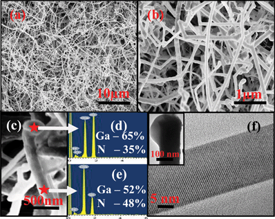 | ||
| Fig. 1 (a and b) FESEM images of entangled GaN NWs grown under atmospheric pressure. (c) Shows a metal droplet on the tip of the nanowire. Elemental analysis (EDX) of GaN nanowire on the (d) droplet of the wire and (e) body of the wire. (f) HRTEM image recorded on the body of a NW shows visible fringes. Inset shows the Ga-droplet on the tip of the NW. | ||
On the other hand, when the similar growth process takes place at the reduced pressure of ∼200 Torr, the structure completely changes from entangled to quasi-aligned vertical NWs with an average diameter of 160 nm and length of 3 μm as shown in Fig. 2(a) and 2(b). Fig. 2(c) shows the top view of a single GaN NW exhibiting the absence of a Ga droplet. The compositional analysis on the tip of the wire confirms the absence of pure Ga or Ga rich GaN (Fig. 2(d)). The EDX spectra recorded on the tip and body of the NW remain identical ((Fig. 2(e)). A HRTEM image of a vertical standing GaN NW is shown in Fig. 2(f) and the inset of the TEM image clearly indicates the NW is straight and smooth with a uniform diameter. The visible lattice fringes on the HRTEM image of the NW illustrate its high crystalline quality without any sheathed amorphous layers. The inter planar spacing is about 0.268 nm (c = 0.536 nm) and confirms the NWs growth along the c-direction.15
 | ||
| Fig. 2 (a and b) FESEM images of vertical aligned GaN NWs grown under reduced (200 Torr) pressure. (c) Focused view of the tip of the nanowire where there is no trace of any metal catalyst. Elemental analysis (EDX) of GaN nanowire on the (d) tip of the vertical wire and (e) body of the wire. f) HRTEM image of a single GaN nanowire grown by the VS route. | ||
When the reactor is kept at the reduced pressure (200 Torr), the Ga metal beam will be carried away partly by the nitrogen gas and maintains thermodynamic equilibrium. Once the NH3 is exposed the entire metal Ga droplet is expected to be converted into GaN nanodots due to the scarcity of Ga which forbids accumulation of Ga liquid droplets on GaN. The GaN nanodot acts as the seed (or) nucleation for the subsequent growth of GaN NWs. The position of the NW is dictated by the Ga metal droplet and the size of the nanodot restricts the diameter of the NW. The continuous supply of Ga through carrier gas and NH3 at constant flow rate facilitates the further growth of the GaN nucleation to form the vertical standing NWs through the vapor–solid (VS) reaction. The growth rate of vertical GaN NWs is greatly reduced as compared to the entangled NWs in the VLS approach due to absence of liquid catalyst on the tip. This slower growth rate is presumably as a result of weaker surface reactivity of vapor–solid interaction over vapor–liquid interaction in VLS growth. The NWs growth under reduced pressure lead to columnar structure with neither liquid nor solid catalyst on the tip. Hence it is very difficult to reiterate the nature of the catalyst involved in the VS mechanism. However, the microscopic and compositional analysis envisages that no catalyst is involved in the growth of NWs under direct VS transformation. The presence or absence of catalyst depends on temperature and precursor pressure which does not hinder the NWs growth but transits the growth structure between entangled and vertical standing wires governed by the VLS and VS mechanism, respectively. It clearly reiterates that regardless of the state of the catalyst NWs continue to grow along the c-axis of GaN but the growth mode strongly transits under reactor pressure.17 Taking a deep insight in the growth mode of GaN NWs, when the reactor is in atmospheric pressure the growth is governed by the VLS mechanism and while the reactor is kept at reduced pressure (200 Torr) the growth is likely driven by VS mechanism.
The schematic representations of the growth mechanism for the entangled and vertical GaN NWs are illustrated in Fig. 3(a) and 3(b) respectively. From the illustration it is apparent that the change in pressure could affect the formation of NWs from the initial nucleation stage where for atmospheric pressure, Ga rich nucleation is formed and the subsequent growth proceeds via the VLS mechanism. For low pressure, GaN nucleation is free from catalysts and the growth is expected to be via the VS route. However, in situ analysis of the growth is required to exactly reiterate the absence of a catalytic adlayer on the NWs during the growth.
 | ||
| Fig. 3 (a) Schematic representation of entangled GaN NW growth under atmospheric pressure governed by the VLS mechanism (b) quasi-aligned vertical standing GaN NWs under reduced pressure which follows VS transformation. | ||
Fig. 4 shows the axial diameter distribution plot for vertical standing NWs which shows the tapering effect of NWs with an average length of ∼2.5 μm that corresponds to the adatom diffusion length of Ga. It is evident that the growth of GaN NWs has the contribution from both the direct impingement and surface diffusion of adatoms upto 2.5 μm and the thinning of the NWs occurs at above 2.5 μm due to diffusion limited growth. Short NWs do not show any tapering and the axial diameter distribution is homogeneous throughout the length (∼2 μm). The initial nucleation associated with the diameter and growth rate of NWs will be presented in the forthcoming article.
 | ||
| Fig. 4 Axial diameter distribution plot for vertical standing NWs indicates two different growth regimes, 1. diffusion induced and 2. direct impingement. | ||
The wurtzite structure (space group C46v) of GaN consists of two formula units per primitive cell. According to the space group analysis, single crystal GaN possesses eight sets of optical phonon modes near the zone center. These modes are classified into Raman active modes (A1 + E1 + 2E2). The phonons of A1 and E1 symmetry are polar, hence the transverse-optical (TO) and longitudinal-optical (LO) phonons of the GaN exhibit different frequencies. Figure 5 shows the μ-Raman spectra of GaN NWs recorded in Z(X,-)![[Z with combining macron]](https://www.rsc.org/images/entities/char_005a_0304.gif) quasi-back scattering geometry. In order to eliminate the dominance of a silicon phonon peak (521.2 cm−1) measurement was broken between 500–530 cm−1. The spectra reveal the symmetry-allowed E2H and A1(LO) modes of GaN.18
quasi-back scattering geometry. In order to eliminate the dominance of a silicon phonon peak (521.2 cm−1) measurement was broken between 500–530 cm−1. The spectra reveal the symmetry-allowed E2H and A1(LO) modes of GaN.18
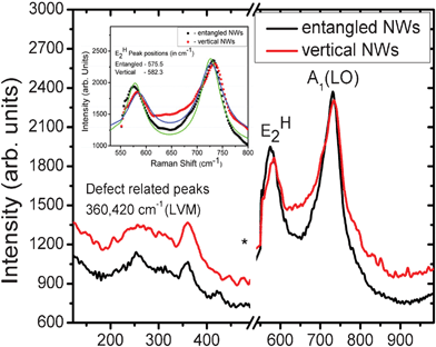 | ||
| Fig. 5 μ-Raman spectra of GaN NWs grown under atmospheric and reduced pressure. Inset shows the Lorentzian fitting for E2H and A1(LO) peaks. | ||
The E2H phonon peaks observed at 575.5 and 582.3 cm−1 for entangled and vertical NWs respectively, are red shifted as compared to strain free GaN (567.6 cm−1). We strongly believe that the E2H phonon mode is from the GaN NWs and not from the interfacial parasitic layer. If the interfacial parasitic layer between the substrate and the NWs contributes to the shift in E2H, it will also induce asymmetric peak broadening and a higher shift in the A1(LO) mode. However, we could not find any considerable peak broadening and shift in the A1(LO) mode. Hence, the red shifts of E2H Raman mode can be attributed to the residual strain in the GaN NWs. This is well corroborated by the interplanar spacing of c-axis oriented GaN NWs revealed by HRTEM analysis. The difference in E2H mode for entangled and vertical GaN NWs (∼7 cm−1) reflects the degree of residual strain present in NWs grown with different growth parameters for the VLS and VS approach. A sharp and intense A1(LO) peak at 728.3 and 730.4 cm−1 for entangled and vertical NWs respectively, was attributed to the uncoupled nature of LO phonon with plasmon due to low free carriers in GaN NWs.19 The difference in peak position of A1(LO) mode (∼2 cm−1) between the entangled and vertical is due to the difference in carrier concentration between the two types of NWs . The peaks at 360 and 430 cm−1 were assigned to local vibration modes due to N or Ga vacancies.20
Temperature dependent photoluminescence for entangled and vertical standing GaN NWs recorded at 10 K and 300 K are shown in Fig. 6(a) and 6(b), respectively. Lorentz deconvoluted spectra show strong ultraviolet near band edge emission (NBE)21 at 3.421 eV and 3.395 eV for entangled and vertical NWs respectively. At 10 K, peaks observed at 3.459 eV and 3.450 eV with the FWHM of 145 meV and 153 meV for entangled and vertical aligned NWs respectively were attributed to donor-bound exciton (DBE) recombination of GaN. In addition to the DBE peak, blue luminescence (BL), green luminescence (GL) and yellow luminescence (YL) were also present in both types of the NWs. The presence of strong BL band can be attributed to the VGa-related complex defects, in particular VGaON and VGaHN.21 Entangled GaN NWs do not show any considerable change in intensity for BL, GL and YL bands for various temperatures (10 K and 300 K).
 | ||
| Fig. 6 Variable temperature photoluminescence spectra of GaN NWs (a) entangled and (b) vertical. | ||
However, the intensity of BL quenches at room temperature for vertical GaN NWs. It has been reported that for undoped GaN the BL band starts to quench at elevated temperature (<200 K). The quenching of the BL band (Fig. 6(b)) is believed to be caused by the escape of holes from the acceptor to the valence band. In vertical standing NWs, the surface impurities at 3.34 eV are assigned to be the surface to bound exciton transition and are expected to increase sharply with the large surface area/aspect ratio of NWs.22,23 However, this band is very weak in entangled NWs due to the random distribution of a wire like mesh. In most of the unintentionally and intentionally doped n-type GaN samples grown by the various techniques, the room-temperature PL spectrum contains a YL band at 2.20–2.25 eV.21 Here, for both the entangled and vertical GaN NWs, the peak at 2.21 eV is observed which is the characteristic nature of GaN and can be attributed to the VGa and related complex defects.21 The decrease in YL intensity of vertically aligned NWs is associated with the absence of coalescence induced defects. For vertical NWs (Fig. 6 (b)), the observed change in the intensity of the YL band corresponds to the BL band owing to the redistribution of holes from the BL-related acceptor to valence band.21 However, a detailed temperature dependent PL measurement is warranted for the further investigation of the nature of BL and GL emission. The self-catalytic assisted growth of entangled and quasi-aligned vertical standing GaN NWs demonstrate good optical and crystalline quality as compared to the catalytic growth of NWs by thermal CVD.24,25
Conclusions
In summary, we have shown the transition of GaN growth structure from entangled NWs to morphologically superior quasi-aligned vertical standing NWs by varying the reactor pressure between atmospheric and 200 Torr. The quasi-aligned vertical standing GaN NWs oriented along the c-axis is governed by the VS mechanism under reduced pressure as opposed to VLS under atmospheric reactor pressure. The results demonstrate that the reactor pressure, which is generally not considered as a key factor, is actually crucial in determining the growth mode and by altering the pressure it is possible to achieve vertical standing self-assembled catalyst free GaN nanowires.Acknowledgements
Authors V.P and K.J thank the Department of Science and Technology (DST), Govt. of India for the financial assistance under project No. SR/FTP/PS-64/2007 and SR/NM/NS-77/2008. The authors acknowledge Dr P.V. Satyam, Institute of Physics, Bhubaneswar, India for TEM measurements. The authors thank Ms. P. Sangeetha, Department of Laser Studies, School of Physics, and Madurai Kamaraj University, Madurai, India for the technical assistance on the μ-Raman measurements.References
- J. C. Johnson, H. J. Choi, K. P. Knutsen, R. D. Schaller, P. Yang and R. J. Saykally, Nat. Mater., 2002, 1, 106 CrossRef CAS.
- P. D. Ye, B. Yang, K. K. Ng, J. Bude, G. D. Wilk, S. Halder and J. C. M. Hwang, Appl. Phys. Lett., 2005, 86, 063501 CrossRef.
- F. Qian, S. Gradecak, Y. Li, C. Y. Wen and C. M. Lieber, Nano Lett., 2005, 5, 2287 CrossRef CAS.
- V. Kumar, D. H. Kim, A. Basu and I. Adesida, IEEE Electron Device Lett., 2008, 29, 18 CrossRef CAS.
- Y. Huang, X. Duan, Y. Cui and C. M. Lieber, Nano Lett., 2002, 2, 101 CrossRef CAS.
- R. S. Wagner and W. C. Ellis, Appl. Phys. Lett., 1964, 4, 89 CrossRef CAS.
- C.Y. Wen, M. C. Reuter, J. Bruley, J. Tersoff, S. Kodambaka, E. A. Stach and F. M. Ross, Science, 2009, 326, 1247 CrossRef CAS.
- J. E. Allen, E. R. Hemesath, D. E. Perea, J. L. L. Falk, Z.Y. Li, F. Yin, M. H. Gass, P. Wang, A. L. Bleloch, R. E. Palmer and L. J. Lauhon, Nat. Nanotechnol., 2008, 3, 168 CrossRef CAS.
- Y. Chen, X. Cui, K. Zhang, D. Pan, S. Zhang, B. Wang and J. G. Hou, Chem. Phys. Lett., 2003, 369, 16 CrossRef CAS.
- M. He, I. Minus, P. Zhou, S. N. Mohammed, J. B. Halpern, R. Jacobs, W. L. Sarney, L. S. Riba and R. D. Vispute, Appl. Phys. Lett., 2000, 77, 3731 CrossRef CAS.
- B. W. Jacobs, M. A. Crimp, K. McElroy and V. M. Ayres, Nano Lett., 2008, 8, 4353 CrossRef CAS.
- E. I. Givargizov, J. Cryst. Growth, 1975, 31, 20 CrossRef CAS.
- H. Li, A. H. Chin and M. K. Sunkara, Adv. Mater., 2006, 18, 216 CrossRef CAS.
- N. Takeuchi, A. Selloni, T. H. Myers and A. Doolittle, Phys. Rev. B: Condens. Matter Mater. Phys., 2005, 72, 115307 CrossRef.
- X. Duan and C. M. Lieber, J. Am. Chem. Soc., 2000, 122, 188 CrossRef CAS.
- L. Yu, N. Liu, X. Wang and Z. Hu, J. Alloys Compd., 2009, 478, L-21 CrossRef CAS.
- S. Kodambaka, J. Tersoff, M. C. Reuter and F. M. Ross, Science, 2007, 316, 729 CrossRef CAS.
- K. Jeganathan, R. K. Debnath, R. Meijers, T. Stoica, R. Calarco, D. Grützmacher and H. Lüth, J. Appl. Phys., 2009, 105, 123707 CrossRef.
- M. Holtz, M. Seon, T. Prokofyeva, H. Temkin, R. Singh, F. P. Dabkowski and T. D. Moustakas, Appl. Phys. Lett., 1999, 75, 1757 CrossRef CAS.
- H. Harima, J. Phys.: Condens. Matter, 2002, 14, 967 CrossRef.
- M. A. Reshchikova and H. Morkoc, J. Appl. Phys., 2005, 97, 061301 CrossRef.
- O. Brandt, C. Pfüller, C. Chèze, L. Geelhaar and H. Riechert, Phys. Rev. B: Condens. Matter Mater. Phys., 2010, 81, 045302 CrossRef.
- J. B. Schlager, K. A. Bertness, P. T. Blanchard, L. H. Robins, A. Roshko and N. A. Sanford, J. Appl. Phys., 2008, 103, 124309 CrossRef.
- J. Yoo, Y. J. Hong, S. J. An, G. C. Yi, B. Chon, T. Joo, J. W. Kim and J. S. Lee, Appl. Phys. Lett., 2006, 89, 043124 CrossRef.
- S. C. Lyu, O. H. Cha, E. K. Suh, H. Ruh, H. J. Lee and C. J. Lee, Chem. Phys. Lett., 2003, 367, 136 CrossRef CAS.
| This journal is © The Royal Society of Chemistry 2012 |