Improvement in CO sensing characteristics by decorating ZnO nanorod arrays with Pd nanoparticles and the related mechanisms
Chia-Ming
Chang
a,
Min-Hsiung
Hon
ab and
Ing-Chi
Leu
*c
aDepartment of Materials Science and Engineering, National Cheng Kung University, 1, Ta-Hsueh Road, Tainan, 701, Taiwan, ROC
bResearch Center for Energy Technology and Strategy, National Cheng Kung University, 1, Ta-Hsueh Road, Tainan, 701, Taiwan, ROC
cDepartment of Materials Science, National University of Tainan, 33, Sec.2, Shu-Lin St., Tainan, 700, Taiwan, ROC. E-mail: icleu@mail.mse.ncku.edu.tw; Fax: 886-6-2380208
First published on 2nd February 2012
Abstract
Pd nanoparticle functionalized ZnO nanorod arrays are produced by the simple and convenient solution routes of aqueous chemical growth and successive photochemical reduction. In this study, we demonstrate the mechanism of the change of surface states and localized electronic properties of Pd/ZnO NRs to account for the enhanced gas sensing performance, as these are often mentioned in association with superior properties, although no firm links have been proved. A significant enhancement in the CO gas sensing properties of ZnO nanorod arrays can be achieved by decorating Pd nanoparticles on the ZnO nanorod surface, and this improvement is ascribed to both the accelerated sensing reaction due to the emergence of a spillover effect, and the amplification of the resistance variation by the enlargement of the Schottky barrier height. These phenomena originate from catalytic Pd acting as a promoter of oxygen adsorption on the ZnO surface, and the transition between metallic Pd and Pd2+/Pd0 redox couple being accompanied by a variation in the work function.
Introduction
The ZnO-based gas sensors are the surface-controlled type, where the dimensions, surface states and quantities of adsorbed oxygen all influence the gas sensing performance significantly.1,2 In addition, the electrical properties of one-dimensional (1D) ZnO nanostructure arrays are exceedingly sensitive to the adsorbed species, because their high surface-to-volume ratio allows the surface atoms to have more opportunities to participate in the surface reactions. Moreover, the gas analyte can diffuse easily throughout the whole sensing component (each nanorod) in this kind of device. Accordingly, ZnO nanorod/nanowire arrays have been extensively used for research in sensing many gas analytes, including O2, H2, C2H5OH, CO, NH3, and so on.1,3–4 In recent years, considerable efforts have been devoted to improve the gas-sensing performance of such devices by facilitating the chemical reaction between the analyte gas and the adsorbed oxygen species (O−,O2− or O−2) on the surface of ZnO nanostructures, which subsequently amplifies the electron transduction signal. The methodologies used to achieve this include constructing hierarchical structures,5 the formation of p–n or n–n heterojunction structures,6,7 and surface functionalization of noble metals.8,9Among these approaches, loading noble metals onto ZnO nanostructures as a sensitizer or promoter has been considered a highly efficient strategy to accelerate the chemical reaction and enhance the gas-sensing performance.
Several methods for the preparation of noble metal-functionalized semiconductors have been reported, such as conventional impregnation,10 wet-chemical reduction,11chemical vapor deposition, sputtering,12,13 and photochemical deposition.14 Although the conventional methods of impregnation and reduction are relatively simple, they show little promise because of the co-deposition of impurities, large distribution of particle size, and difficulty in controlling the particle density. Although the gas-phase approaches offer some ways to overcome these drawbacks, they suffer from other inherent weaknesses, such as high processing cost and complex manipulation conditions. In this article, we report results for the deposition of Pd nanoparticles as catalysts by photochemical reduction on ZnO nanorod arrays to improve the gas sensing performance. The advantages of this approach is its convenience, time-saving and has no need for pre-functionalization of the ZnO support or pre-synthesis of the noble metals. It is noted that the photochemical reduction method presented in this work should be the most suitable and cost-effective approach for attaching noble metal nanoparticles to 1D semiconducting nanostructure arrays, particularly in comparison with impregnation and sputtering. In addition, a sensing test is performed using carbon monoxide as the probe gas to evaluate the sensing properties of the gas sensors. A compact CO gas sensor is required to monitor the carbon monoxide in exhaust gas from the use of gasoline and natural gas due to incomplete combustion. Most importantly, excess CO gas in a sealed environment is a severe threat to personal safety, especially due to its characteristics of being colorless and odourless, and thus more effective sensors are urgently required.
The decoration of palladium on SnO2-based nanostructures is widely employed to detect CO and H2 gases, and the sensing mechanism is usually attributed to the enhancement of the electron depletion layer, which involves a PdO crystallite.15,16 However, the Pd/SnO2 occasionally exhibits p-type sensing behavior with regard to CO gas,17,18 and thus this kind of composite is unfavourable for use in CO sensing applications due to the complexity and instability in signal identification. Recently, Pd/ZnO nanofibers have been used for gas sensing with considerable sensitivity, rapid response, and good selectivity for low concentrations of CO.19 The promoting mechanism is ascribed to the PdO, as reported in the case of SnO2, but as yet there remains no definite evidence to support this speculation. Xing et al. proposed that the Pd/ZnO nanoflowers exhibit good sensing performance as a result of the catalytic activity of Pd nanoparticles and the variation in barrier height at Pd/ZnO interface.9 However, the metallic Pd decorated on the ZnO surface should maintain the Schottky contact barrier at the Pd/ZnO interface due to the difference in work function between them. According to a survey of the literature, the effects of Pd nanoparticles on a ZnO-based gas sensor are still controversial, the actual sensing mechanisms related to Pd/ZnO gas sensors require further study. Our results clearly demonstrate that the Pd/ZnO NRs possess superior CO gas sensitivity, response and recovery time to those of the pristine ZnO NRs. In addition, the promoting mechanism is based on the cooperation of chemical and electronic sensitization, according to the interpretation of the XPS and TEM results obtained in this work.
Experimental procedures
The pristine ZnO nanorod arrays were grown on a sol–gel derived seed layer through an aqueous chemical growth (ACG) method. The sol–gel solution was prepared as the precursor for coating the substrates with a ZnO seed layer by dissolving Zn(CH3COO)2·H2O in ethanolamine and 2-methoxyethanol solutions at room temperature. The molar ratio of ethanolamine to zinc acetate was kept at 1.0, and the concentration of zinc acetate was 2.0 M. The resulting solution was stirred at 60 °C for 2 h to yield a clear and homogeneous solution. A pair of interdigital Au/Cr electrodes was deposited on the silica by electron beam evaporation through photolithography and lift-off processes, with a 50 μm gap between adjacent electrodes. The precursor solution was dropped onto the interdigital electrode and coated by a spinner, and then the substrates were dried at 300 °C for several minutes until the solvent was evaporated. The resulting substrates with sol–gel film were used for growing ZnO nanorod arrays after annealing at 500 °C for 1 h to form ZnO seed layers. The aqueous chemical growth was performed by suspending the substrates with a sol–gel-derived seed layer into the Zn salt (zinc nitrate hexahydrate)/ HMTA (hexamethylenetetramine) solution at 95 °C for 3 h. The ACG solution was composed of 0.025 M Zn(NO3)2·6H2O and C6H12N4. The ZnO nanorod arrays rooted in the substrate were washed with distilled water several times, and dried at 60 °C. The synthesis of Pd/ZnO NRs was performed through immersion of ZnO NRs into the palladium chloride–ethanol solution at room temperature under an ultraviolet lamp (365 nm, around 5.3 mW cm−2) irradiation for 30 min. A palladium precursor solution with a light yellow color was obtained by dissolving 0.75 mM PdCl2 in anhydrous ethanol with vigorous stirring for 30 min. During the photochemical reduction processes, the Pd nanoparticles were deposited and reduced on the surface of ZnO nanorods. After this, the Pd/ZnO NRs were acquired by washing with distilled water, blowing with N2 gas, and drying at 60 °C.The SEM images and EDS spectra of the samples were obtained using a high resolution and field-emission scanning electron microscope (Hitachi S4200 HR-SEM and Philips XL40 FE-SEM). The structures of the samples were identified by a grazing incident angle X-ray diffractometer (GA-XRD) (RIGAKU D/MAX2500) with a scan speed of 4°/min and a scan step of 0.01°. The TEM images and the localized diffraction patterns of the Pd/ZnO nanorods were captured using an ultra-high resolution analytical electron microscope (JEOL-2100F CS STEM). The XPS data were collected in a PHI 5000 ESCA system and the recorded XPS spectra were processed using the Xpspeak41 software. The background of the spectra was subtracted using the Shirley method and decomposed using Gaussian–Lorentzian sum functions. The layout of the ZnO sensing device was depicted in an earlier article, and the details of the gas detection system with a digital multimeter (Agilent 3458A) have also been described previously.2,20 The gas sensing properties were evaluated at specific temperatures by measuring the variation in resistance of the sensors under ambient gas (air) conditions and CO–mixed air conditions. The measurements were carried out at a bias voltage of 5 V.
Results and discussion
Fig. 1 (a) and (b) show SEM images and the corresponding EDS spectra of the blank ZnO nanorod arrays and Pd functionalized ZnO nanorod arrays (Pd/ZnO NRs), respectively, which indicate the existence of palladium species on the ZnO nanorods. The diameters of the ZnO nanorods are tens of nanometres (50∼85 nm), and the nanorods are mostly perpendicular to the sol–gel-derived seed layer. The cross-sectional views of the ZnO and Pd/ZnO nanorod arrays are shown in Fig. 1 (c) and (d), and the corresponding backscattered electron (BSE) images clearly reveal that the palladium nanoparticles are attached to the elongated ZnO nanorods with a size of several hundred nanometres (600∼700 nm). However, the diameters of ZnO nanorods decorated with Pd nanoparticles are a little smaller than those of the pristine ZnO NRs, because there is a slight dissolution reaction prior to the photochemical reduction for palladium ion attachment. When the ZnO nanorods are immersed in the precursor solution, the Cl− ions have an opportunity to adsorb on the ZnO surface and react with zinc to form a complex with a Zn(II) cation.21 Accordingly, the zinc atoms become quite easy to dissociate from the ZnO lattice, which causes the dissolution seen in the present system.22 The remaining surface oxygen atoms attract the palladium ions in bulk solution by electrostatic interaction, and the Pd(II) ions are then adsorbed on the ZnO surface and subsequently reduced to metallic palladium by photochemical reduction. Actually, the photocatalytic activities of ZnO-based materials are well known, and which have also been used to reduce Pd(II) ions acting as active sites for the electroless plating of copper on patterned areas.23 When ZnO is exposed to UV light, the photo-induced electron–hole pairs are generated. In the presence of ethanol the holes are scavenged to produce ethoxy radicals, leaving the electrons to accumulate within the ZnO nanorods. Consequently, the accumulated electrons can reduce Pd(II) ions on the ZnO surface according to the following reaction: | (1) |
| ZnO(e−) + Pd2+ → Pd0 + ZnO |
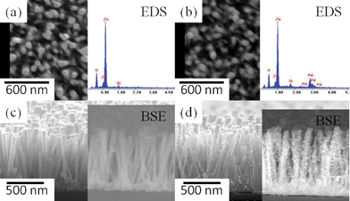 | ||
| Fig. 1 The SEM images of (a),(c) pristine ZnO nanorod arrays and (b),(d) Pd/ZnO NRs fabricated by photochemical reduction in 0.75 mM PdCl2 ethanol solution. The corresponding EDS spectra and BSE images are also shown. | ||
Therefore, the palladium nanoparticles are deposited on ZnO nanorods, which is confirmed by the grazing angle X-ray diffraction pattern shown in Fig. 2. The GA-XRD pattern shows that the as-synthesized ZnO nanorod arrays have a Wurtzite (hexagonal) structure with lattice constants of a = b = 0.32 nm, c = 0.52 nm. All of the diffraction peaks can be well-indexed to the standard pattern of ZnO (JCPDS 36-1451). In addition, the presence of a diffraction peak at 39.31° for the Pd/ZnO nanorod arrays can be indexed to the metallic Pd (111) crystal plane (JCPDS 87-0641).
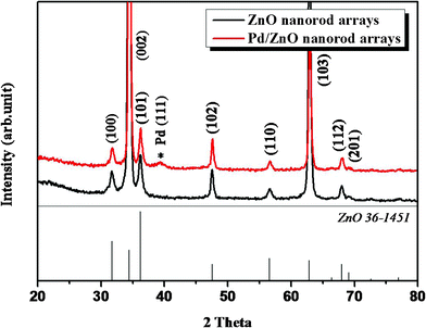
Fig. 3(a) shows a low magnification TEM image of ZnO nanorods with Pd nanoparticles attached on their surfaces. It is noted that the spherical palladium nanoparticles tend to agglomerate on the surface of the ZnO nanorods, and the primary nanoparticles in the clusters have a particle size of around 5 nm. In the localized HR-TEM images shown in Fig. 3 (b) and (c), the measured d-spacing of 0.262 nm between adjacent lattices planes is consistent with the distance between two (002) crystal planes of ZnO. On the other hand, the images also reveal that the palladium nanoparticles have a clear lattice fringe of 0.23 nm spacing, which is similar to the Pd (111) lattice spacing. Moreover, the corresponding electron diffraction pattern of the palladium nanoparticles on the ZnO is inserted at the top right corner of Fig. 3(c), which further confirms the single-crystal nature of Pd nanoparticles, with no evidence of bulk oxidation despite their small size and exposure to air during sample preparation. The numerous Pd nanoparticles gathered as clusters on the ZnO surface maybe due to the high surface energy produced by the surface effect of nanocrystals with a small feature size.1 As reported in the literature, the formation mechanism of Pd clusters on the SnO2 surface is because of the instability of the stacking of palladium layers when the deposits attain about 3.5 and 6.5 monolayers.24 In addition, with regard to the synthesis of Ag and Au nanostructures in ionic liquid, it has been reported that a longer reaction time leads to the dominant cluster morphology in the kinetic control processes.25 The agglomeration of palladium nanoparticles could be modulated by using a capping agent (like poly(vinyl pyrrolidone), PVP) to lower the interfacial energy of individual nanoparticles, or by manipulating the process parameters to optimize the deposition behavior, and these topics are subject to ongoing investigation. Even though many Pd nanoparticles aggregate on the ZnO surface, they are still able to promote the gas sensing performance due to their catalytic activity, as will be discussed later.
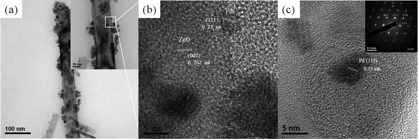 | ||
| Fig. 3 (a) The low-magnification TEM image and (b) (c) high resolution TEM images of the Pd nanoparticles decorated ZnO nanorod. The insert of (c) is the corresponding electron diffraction pattern of a Pd nanoparticle on the ZnO nanorod. | ||
In order to examine the role of palladium nanoparticles when decorated on ZnO NRs used for sensing carbon monoxide, XPS analysis was performed to probe the chemical states of the nanoparticles and NRs and to explore the interaction between Pd and ZnO. In Fig. 4 (a), the O 1s core level spectra of blank ZnO NRs and Pd/ZnO NRs are partitioned into three parts (denoted as O1, O2 and O3) by multiple peaks fitting. The lower energy peaks (O1) at 530.35 ± 0.3 eV can be assigned to O2− ions in the Wurzite structure of the ZnO lattice surrounded by Zn atoms with their full complement of nearest-neighbor O2− ions.26,27 The medium energy component (O2) at 531.31 ± 0.3 eV is attributed to O2− ions in the oxygen-deficient regions with the matrix of ZnO (ZnOx), or the presence of OH bonds, namely ZnO(OH).26,27 The higher energy peak (O3) at 532.25 ± 0.3 eV is usually associated with the specific chemisorbed oxygen on the surface of ZnO, such as –CO3, adsorbed O2, or adsorbed H2O.26,27 The adsorbed O2 can be functionalized as the ionsorbed oxygen (O−, O2−or O−2) by means of capturing the conduction electrons from ZnO, and consequently reduces the conductivity. It is well-known that the adsorbed oxygen species are the most important factor for gas sensing processes, and therefore their quantity is generally regarded as a key criterion for interpreting the difference in sensing performance. In this work, the amount of adsorbed O2 is estimated through the integrated area ratio of O3 in the O 1s peak in the XPS spectra. As shown in Fig. 4 (a), the ratio of adsorbed O2 in blank ZnO NRs is 10%, which is similar to the reported data for the fraction of surface sites involving charge transfer by oxygen adsorption on SnO2 nanowires.28 Moreover, it shows that the amount of adsorbed O2 in Pd/ZnO NRs is three-fold larger than that in the blank ZnO NRs, which should be due to the dissociation of molecular oxygen facilitated by the palladium nanoparticles and the consequent spill over of atomic oxygen onto the oxide surface.12,13 The XPS spectra for the Pd 3d region are shown in Fig. 4 (b), which provides precise information on the chemical state of the Pd NPs on the ZnO nanorod arrays. The gap between the level of Pd 3d5/2 and Pd 3d3/2 is similar to the spin–orbit doublet separation value (5.3 eV) reported in the literature.29Fig. 4 (b) shows that the Pd 3d5/2spectra have three characteristic peaks with binding energies of 334.4, 335.1 and 336.3 eV, which can be individually identified as surface Pd0 atoms, bulk metallic Pd0 and Pd2+ (PdO) respectively.30,31 For the Pd supported on the ZnO surface, the variation in structural characteristics could lead to the binding energy of Pd 3d5/2 with a negative shift against the bulk value.32 This is because of an increase in final state screening coming from the agglomeration of the Pd film to form three-dimensional clusters, where the proportion of under-coordinated step edges increases significantly.32 The surface Pd0 atoms in the present study are thus ascribed to the agglomeration of some palladium nanoparticles with a lower coordination number than the bulk atoms. In addition, the chemisorbed oxygen bonds with Pd form a Pd2+–O2− surface dipole, due to the charge transfer from palladium to oxygen atoms caused by the discrepancy in electron affinity. This extra potential energy difference will limit the electrons flowing out of the Pd, resulting in an increase in work function and binding energy of Pd. This result corresponds to the higher binding energy peak in the Pd 3d5/2 associated with Pd2+ (PdO). In addition, the coexistence of metallic Pd0 and Pd2+ forms a redox couple of Pd2+/Pd0 with a larger work function than metallic Pd.33 Furthermore, the Pd2+ (PdO) component in the XPS spectra reduces significantly when this redox couple is exposed to 100 ppm CO in synthetic air.18 The Pd2+ (PdO) signal is thus inferred as being due to the ionsorbed oxygen coordinating with the Pd surface in the present study, and the results of the XRD and TEM analyses in particular demonstrate the presence of Pd crystals rather than PdO (palladium oxide).
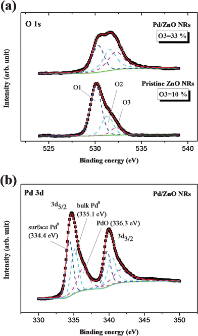 | ||
| Fig. 4 The XPS of (a) the O 1s core levels obtained from pristine ZnO nanorod arrays and Pd/ZnO NRs (b) the Pd 3d core levels acquired from Pd/ZnO nanorod arrays. (The spectra were calibrated using the C 1s core level associated with carbon pollution at 284.6 eV as a reference.) | ||
Fig. 5 (a) shows the variation in sensitivity in both blank ZnO NRs and Pd/ZnO NRs to different concentrations of mixed carbon monoxide (CO) gas (with air) under their respective optimum operating temperatures. The optimal operating temperatures for blank ZnO NRs and Pd/ZnO NRs are 260 °C and 300 °C, respectively, which is determined by a comparison of their sensitivities to 500 ppm CO gas at different operating temperatures (data not shown here). The sensitivity is defined as the ratio of Rair to Rco, where Rair and Rco represent the resistances of a ZnO based sensor in air and in the air–carbon monoxide mixed ambient gas, respectively. The insert in Fig. 5 (a) shows the time dependence of change in resistance in these two gas sensors, as the gas ambient is sequentially switched from air to various concentrations (10 ppm∼600 ppm) of air–carbon monoxide and back to air. When the ZnO is exposed to air at moderate temperature, the oxygen adsorbed on ZnO surface will act as an electron acceptor. The adsorbed oxygen species will capture electrons from ZnO to form ionsorbed oxygen (O− or O2−) through binding at the oxygen deficient areas, which leads to surface depletion in the conductance channel of ZnO. The carrier concentration in the ZnO is decreased and the surface depletion layer is widened, both giving rise to an increase in resistance. When exposed to a reducing gas, the reactions between the reducing gas and ionsorbed oxygen on the surface will result in the desorption of adsorbed oxygen, as well as the release of the trapped electrons, which causes a decrease in the depletion width and the resistance in ZnO. Consequently, the change in resistance is mainly caused by the adsorption and desorption of oxygen species on the surface of sensing materials; moreover, the increased range of variation in resistance with the rise in concentration of the reducing gas is also demonstrated in the insert of Fig. 5 (a). It is seen that the gas sensitivity of Pd/ZnO NRs, with an identical CO concentration, can be promoted four to six times compared with those of the blank ZnO NRs in Fig. 5 (a). In addition, the detection limit (defined as the concentration at which the resistance variation is higher than the noise floor) and optimal operating temperature can be reduced to 10 ppm (near the detection limit of commercial sensors) and 260 °C, respectively, by anchoring Pd NPs on ZnO NRs. Xing et al. reported that the Pd/ZnO nanoflowers exhibit outstanding sensitivity to ethanol gas, but nearly no response to CO gas.9 This difference is because the electron donation effect of ethanol is stronger than that of CO, as indicated by the following equations:5
| CO + O−(ad) → CO2 + e− |
| CH3CH2OH + 6O−(ad) → 2CO2 + 3H2O + 6e− |
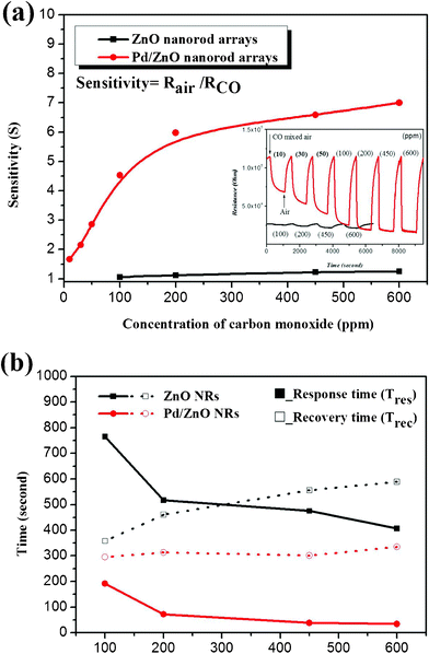 | ||
| Fig. 5 (a) The variation in sensitivity when the pristine ZnO NRs and Pd/ZnO nanorod arrays were exposed to various air–carbon monoxide mixed ambient gases at individual optimal operating temperatures (300 °C and 260 °C). The insert is the transient resistance change of pristine ZnO NRs and Pd/ZnO NRs under different CO concentrations. (b) The response and recovery times to various concentrations of CO in pristine ZnO and Pd/ZnO NRs gas sensors. | ||
The gas sensitivity to ethanol gas is thus often higher than that of CO gas at the equivalent concentration, no matter whether the ZnO nanostructures have been decorated with noble metals or not, as reported in the literature.5,9,34 According to Zhang et al.,34 the ethanol sensitivity of ZnO nanowires can be improved by anchoring Pd nanoparticles to them, which indicates that the sensitization of Pd works. The fact that CO sensitivity of Pd/ZnO nanowires cannot be effectively promoted may be due to the incomplete reaction of adsorbed oxygen with CO. In our study, the Pd/ZnO NRs have a 3-D structure, where the CO can diffuse easily throughout the whole sensing component (each nanorod). Accordingly the CO sensitivity increases significantly. However, the electron donation effect is not the only influential factor with regard to gas sensitivity, and others, such as reactions between the testing gases and sensing material, or humidity, may exist and compete against each other. The former can be regarded as a gas selectivity problem, and the latter is diminished at such a high operating temperature. In a study by Hsueh et al.,35 where the Pd nanoparticles were also attached to the ZnO nanostructure arrays by photochemical reduction, an ethanol sensor was produced. Consequently, this kind of Pd/ZnO NRs may also have an enhanced sensing capability towards CO gas, and this subject deserves to be investigated in more detail.
According to Fig. 4 (a), the Pd functionalized ZnO NRs possess much more ionosorbed oxygen than the blank ZnO NRs due to the catalytic effect of palladium in dissociating oxygen molecules and causing a spill over of the ionosorbed oxygen on the ZnO surface.12,13 Therefore, the amount of charge carrier shuttling between the ionosorbed oxygen and ZnO nanorods increases markedly during the sensing process. When Pd/ZnO is exposed to the air, the oxygen molecules adsorbed on the palladium surface can capture the free electrons, forming a redox couple Pd2+/Pd0 with an electronic potential located at 5.5 eV below the vacuum level.18,33 The larger work function of the Pd2+/Pd0 redox couple forms a localized Schottky barrier in the vicinity of the Pd/ZnO interface, which increases the height of the barrier and width of depletion region. Consequently, the equilibrium resistance in Pd/ZnO NRs increases as the Schottky barrier present in the Pd–ZnO interface results in a narrowing of the electrical conduction channel, as shown in the insert of Fig. 5 (a). When exposed to CO gas, the reaction between adsorbed oxygen ions and CO molecules will release electrons back to palladium and let Pd2+ partially reduce to Pd0, which reduces the work function of Pd species from 5.5 eV to 5.1 eV.18,33,36 Accordingly, the Fermi level of ZnO shifts upward and pins at the work function of metallic Pd (5.1 eV),36 which greatly lowers the initial Schottky barrier height (depletion layer) in the Pd/ZnO interface (beneath ZnO nanorod surface). Therefore, the numerous trapped electrons are drawn back and the conduction channel is significantly broadened when Pd/ZnO NRs are exposed to CO gas, which causes a noticeable improvement in sensitivity. The schematic band diagrams of pristine ZnO and Pd/ZnO nanorod arrays exposed to both air and CO–mixed air ambient gas are shown in Fig. 6. Even though the Pd/ZnO NRs are exposed to a small dose of CO, the variation in resistance is still discernible by significant modification of barrier height. Accordingly, the detection limit for CO in Pd/ZnO NRs can be decreased to 10 ppm. These improvements in sensing performance are ascribed to a combination of electron sensitization (modification of the Schottky barrier) and the catalytic effect of Pd nanoparticles (spill over effect). Chang et al. also decorated ZnO nanowire arrays with Au nanoparticles by photochemical reduction for CO gas sensing.14 The optimal operating temperature of our Pd/ZnO NRs is similar to that in found in this earlier work, which could be due to the common spill over effect of noble metals on ZnO nanostructures. However, the sensitivity of Pd/ZnO NRs to 50 ppm CO in the present study is higher than that of Au/ZnO nanowire arrays as a result of the additional electron sensitization of Pd nanoparticles.
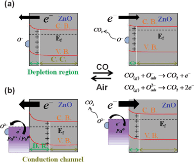 | ||
| Fig. 6 The schematic band diagrams of (a) pristine ZnO NRs and (b) Pd/ZnO nanorod arrays exposed to air and CO gas ambient. (The C.B., V.B. and Ef are the codes of the conduction band, valence band and Fermi level. D.R. and C.C. denote the depletion region and conduction channel.) | ||
The catalytic activity of Pd nanoparticles on a ZnO NRs gas sensor not only contributes significantly to the higher sensitivity and lower detection limit, but also the faster response and recovery time. As shown in Fig. 5 (b), the response and recovery times of ZnO NRs are reduced by 4∼12- and 1∼2-fold, respectively, for different CO concentrations when Pd NPs have been attached. The response time is usually defined as the time needed to reach 90% variation in resistance, as the resistance approached a steady condition upon exposure to the test gas. The recovery time is defined as the time required for resistance to return a 10% variation in resistance in air after stopping the flow of test gas. In terms of response time, the sensing reaction to a reducing gas consists of diffusion of the analyte gas onto the surface of the sensing materials, and its subsequent oxidation by adsorbed oxygens (O− or O2−). Accordingly, the response times in the blank ZnO NRs and Pd/ZnO NRs are both reduced with the increasing CO concentration, because the concentration gradient increases with the amount of analyte gas. In addition, the abundant ionosorbed oxygen coming from the spill over effect of Pd NPs also benefits the oxidation of CO, which results in greatly decreased response times of Pd/ZnO NRs. At the same time, the desorption of oxygen will leave behind vacant states on the ZnO surface, which need to be compensated for by oxygen molecules in the recovery process. The repopulation of ionosorbed oxygen causes the resistance to return the initial value, but this approach has to overcome the activation energy for the adsorption/dissociation of oxygen molecules.37,38 It is thus intuitively considered that a large amount of unoccupied states retard the recovery reactions, and thus the recovery times are increased with the increasing CO concentration in pristine ZnO NRs, as shown in Fig. 5 (b). Although the magnitude of the unoccupied states in Pd/ZnO NRs should be significantly higher than that seen with pristine ones, the recovery times in the former are shorter. This is because the palladium is a far better oxygen dissociation catalyst than the blank ZnO; as a result, the oxygen molecules can be quickly dissociated over the Pd, and the ionsorbed oxygen can more easily diffuse and adsorb on the surface of the ZnO nanorods.9,12 As compared with the results of Wang et al.,39 the improved magnitude in response time of our Pd/ZnO NRs is similar to those of ZnO–CuO composite NWs, which may be because the high surface-to-volume ratio structure is more effectively employed for CO gas sensing. Besides, the recovery time of the present device is about three-fold lower than that of ZnO–CuO composite as a result of the catalytic effect of Pd nanoparticles.
Conclusions
Pd nanoparticles are successfully deposited on the ZnO nanorod arrays by photochemical reduction, and they agglomerate on the ZnO nanorod surface because of the surface effect of nanocrystals. Both the XRD spectrum and TEM diffraction pattern demonstrate that the Pd species on ZnO NRs are the metallic phase, instead of another composition. The Pd2+ (PdO) component in the Pd 3d region of the XPS spectra is thus regarded as the chemisorbed oxygen on the Pd nanoparticles. Owing to the discrepancy in electron affinity, the electron transfer from Pd to O causes the emergence of a Pd2+/Pd0 redox couple with a larger work function than the metallic Pd. The Pd/ZnO NRs exhibit a significant improvement in CO gas sensing performances as compared with the blank ZnO NRs. When the concentration of CO varied from 100 ppm to 600 ppm, the gas sensitivity was raised by 4∼6-fold, and the response and recovery times were reduced by 4∼12- and 1∼2-fold, respectively. These improvements are because of the more ionsorbed oxygen in the Pd/ZnO NRs, as seen in the O 1s spectra, which is due to the enhanced catalytic dissociation of O2 on the surface of the Pd nanoparticles, and the subsequent diffusion of the ionosorbed oxygen to the ZnO nanorod surface. The presence of the Pd2+/Pd0 redox couple results in a significant modification of Schottky barrier height between Pd and ZnO, which effectively enlarges the variation of resistance in Pd/ZnO NRs during the sensing process, even at a lower concentrations of CO. Consequently, the detection limit of Pd/ZnO NRs with regard to CO can be reduced to 10 ppm in comparison with the 100 ppm of blank ZnO NRs.Acknowledgements
The financial support of this study through contracts no. NSC 96-2221-E-006-119-MY3, NSC 98-2221-E-006-075-MY3 and NSC 100-2221-E-006-122-MY3 of the National Science Council, Taiwan ROC is greatly appreciatedReferences
- L. Liao, H. B. Lu, J. C. Li, H. He, D. F. Wang, D. J. Fu, C. Liu and W. F. Zhang, J. Phys. Chem. C, 2007, 117, 1900 Search PubMed.
- C. M. Chang, M. H. Hon and I. C. Leu, Sens. Actuators, B, 2010, 151, 15 CrossRef.
- J. Y. Park, D. E. Song and S. S. Kim, Nanotechnology, 2008, 19, 105503 CrossRef.
- J. X. Wang, X. W. Sun, Y. Yang, H. Huang, Y. C. Lee, O. K. Tan and L. Vayssieres, Nanotechnology, 2006, 17, 4995 CrossRef CAS.
- Y. Zhang, J. Q. Xu, Q. Xiang, H. Li, Q. Y. Pan and P. C. Xu, J. Phys. Chem. C, 2009, 113, 3430 CAS.
- C. W. Na, H. S. Woo, I. D. Kim and J. H. Lee, Chem. Commun., 2011, 47, 5148 RSC.
- J. X. Wang, X. W. Sun, S. S. Xie, Y. Yang, H. Y. Chen, G. Q. Lo and D. L. Kwong, J. Phys. Chem. C, 2007, 111, 7671 CAS.
- X. H. Liu, J. Zhang, X. Z. Guo, S. H. Wu and S. R. Wang, Nanoscale, 2010, 2, 1178 RSC.
- L. L. Xing, C. H. Ma, Z. H. Chen, Y. J. Chen and X. Y. Xue, Nanotechnology, 2011, 22, 215501 CrossRef.
- J. Q. Xu, J. J. Han, Y. Zhang, Y. Sun and B. Xie, Sens. Actuators, B, 2008, 132, 334 CrossRef.
- X. L. Gou, G. X. Wang, J. Yang, J. S. Park and D. Wexler, J. Mater. Chem., 2008, 18, 965 RSC.
- A. Kolmakov, D. O. Klenov, Y. Lilach, S. Stemmer and M. Moskovits, Nano Lett., 2005, 5, 667 CrossRef CAS.
- M. K. Kumar, L. K. Tan, N. N. Gosvami and H. Gao, J. Phys. Chem. C, 2009, 113, 6381 CAS.
- S. J. Chang, T. J. Hsueh, I. C. Chen and B. R. Huang, Nanotechnology, 2008, 19, 175502 CrossRef.
- D. J. Yang, I. Kamienchick, D. Y. Youn, A. Rothschild and I. D. Kim, Adv. Funct. Mater., 2010, 20, 4258 CrossRef CAS.
- S. Banerjee1, A. Bumajdad and P. S. Devi, Nanotechnology, 2011, 22, 275506 CrossRef.
- P. Ménini, F. Parret, M. Guerrero, K. Soulantica, L. Erades, A. Maisonnat and B. Chaudret, Sens. Actuators, B, 2004, 103, 111 CrossRef.
- I. Aruna, F. E. Kruis, S. Kundu, M. Muhler, R. Theissmann and M. Spasova, J. Appl. Phys., 2009, 105, 064312 CrossRef.
- S. H. Wei, Y. Yu and M. H. Zhou, Mater. Lett., 2010, 64, 2284 CrossRef CAS.
- J. F. Chang, H. H. Kuo, I. C. Leu and M. H. Hon, Sens. Actuators, B, 2002, 84, 258 CrossRef.
- J. Domenech and A. Prieto, J. Phys. Chem., 1986, 90, 1123 CrossRef CAS.
- H. Yoshiki, K. Hashimoto and A. Fujishima, J. Electrochem. Soc., 1995, 142, 428 CrossRef CAS.
- H. Yoshiki, H. Kitahara, K. Hashimoto and A. Fujishima, J. Electrochem. Soc., 1995, 142, L235 CrossRef CAS.
- R. Huck, U. Bottger, D. Kohl and G. Heiland, Sens. Actuators, 1989, 17, 355 CrossRef CAS.
- A. I. Bhatt, A. Mechler, L. L. Martin and A. M. Bond, J. Mater. Chem., 2007, 17, 2241 RSC.
- H. H. Wang, S. H. Baek, J. J. Song, J. Y. Lee and S. W. Lim, Nanotechnology, 2008, 19, 075607 CrossRef.
- M. Chen, X. Wang, Y. H. Yu, Z. L. Pei, X. D. Bai, C. Sun, R. F. Huang and L. S. Wen, Appl. Surf. Sci., 2000, 158, 134 CrossRef CAS.
- F. Hernandez-Ramirez, J. D. Prades, A. Tarancon, S. Barth, O. Casals, R. Jimenez-Diaz, E. Pellicer, J. Rodriguez, J. R. Morante, M. A. Juli, S. Mathur and A. Romano-Rodriguez, Adv. Funct. Mater., 2008, 18, 2990 CrossRef CAS.
- G. Polzonetti, M. V. Russo, G. Infante and A. Furlani, J. Electron Spectrosc. Relat. Phenom., 1997, 85, 73 CrossRef CAS.
- R. Massard, D. Uzio, C. Thomazeau, C. Pichon, J. L. Rousset and J. C. Bertolini, J. Catal., 2007, 245, 133 CrossRef CAS.
- J. F. Moulder, Handbook of X-ray photoelectron spectroscopy: a reference book of standard spectra for identification and interpretation of XPS data, Eden Prairie, Minn.: Physical Electronics, 1995 Search PubMed.
- M. P. Hyman, V. M. Lebarbier, Y. Wang, A. K. Datye and J. M. Vohs, J. Phys. Chem. C, 2009, 113, 7251 CAS.
- S. Matsushima, Y. Teraoka, N. Miura and N. Yamazoe, Jpn. J. Appl. Phys., 1988, 27, 1798 CrossRef CAS.
- Y. Zhang, Q. Xiang, J. Q. Xu, P. C. Xu, Q. G. Pan and F. Li, J. Mater. Chem., 2009, 19, 4701 RSC.
- T. J. Hsueh, S. J. Chang, C. L. Hsu, Y. R. Lin and I. C. Chen, Appl. Phys. Lett., 2007, 91, 053111 CrossRef.
- D. F. Gu and S. W. K. Dey, Appl. Phys. Lett., 2006, 89, 082907 CrossRef.
- N. Barsan and U. Weimar, J. Electroceram., 2011, 7, 143 CrossRef.
- S. R. Morrison, The chemical physics of surfaces, 2nd edition, New York : Plenum Press, 1990, p255 Search PubMed.
- J. X. Wang, X. W. Sun, Y. Yang, K. K. AKyaw, X. Y. Huang, J. Z. Yin, J. Wei and H. V. Demir, Nanotechnology, 2011, 22, 325704 CrossRef CAS.
| This journal is © The Royal Society of Chemistry 2012 |