Room-temperature wide-range photoluminescence and semiconducting characteristics of two-dimensional pure metallic Zn nanoplates
Jin-Han
Lin
a,
Yong-Jie
Huang
a,
Yan-Ping
Su
a,
Che-An
Liu
a,
Rupesh S.
Devan
a,
Ching-Hwa
Ho
b,
Yi-Ping
Wang
b,
Hung-Wen
Lee
a,
Chun-Ming
Chang
a,
Yung
Liou
c and
Yuan-Ron
Ma
*a
aDepartment of Physics, National Dong Hwa University, Hualien 97401, Taiwan, R.O.C. E-mail: ronma@mail.ndhu.edu.tw; Fax: +886-3-8633690; Tel: +886-3-8633706
bGraduate Institute of Applied Science and Technology, National Taiwan University of Science and Technology, Taipei 106, Taiwan, R.O.C.
cInstitute of Physics, Academia Sinica, Taipei 11529, Taiwan, R.O.C.
First published on 18th January 2012
Abstract
We explore the structural, electronic, photoluminescent, metallic, and semiconducting characteristics of 2D pure Zn-metal nanoplates. The 2D pure Zn-metal nanoplates are synthesized by the hot-filament metal-oxide vapor deposition (HFMOVD) technique. They have an average diameter and thickness of ∼520 and ∼144 nm, respectively. The results of the electronic and crystalline structure studies reveal the 2D nanoplates to be pure Zn hexagonal crystals, which can provide a wide-range photoluminescence from ultraviolet (UV) to red light emissions at room temperature. The measured valence-band and the calculated band-structure of the 2D pure Zn-metal nanoplates verify that the UV and blue light arise from the 3d–sp interband transitions, while the green, yellow, and red lights come from the valence-conduction interband transitions at a bandgap that is only present in the 2D nanoplates. Therefore, the 2D pure Zn-metal nanoplates possess not only metallic, but also semiconducting characteristics.
A. Introduction
Since Mooradian1 first observed photoluminescence (PL) emissions from pure gold and copper in 1969, PL spectroscopy has become a well-developed optical tool that can be used to examine impurities and defects in semiconductor materials, as well as the radioactive electron transitions between the Fermi level (EF) and 3d-orbital bands in metals. Nowadays, PL studies on pure metals are attracting a great deal of research interest. The majority of such studies have focused on the noble metals including gold (Au),2,3silver (Ag),2,3 and copper (Cu).2,3 However, there have been a few studies investigating the PL emissions of zinc (Zn).4–8 In this current work, we synthesized two-dimensional (2D) pure Zn-metal nanoplates using hot filament metal vapor deposition for applications in optical devices. The technique of hot filament metal vapor deposition has become very prominent because it can be exploited to synthesize 2D Bi-metal nanostructures with different morphologies and crystalline traits,9,10 as well as various metal-oxide nanostructures with different morphologies and crystalline traits.11–20 The superior optical properties of 2D pure metal nanoplates with regular shapes, such as nanoprisms,21 surface plasmon excitations,22,23 and surface-enhanced Raman scattering (SERS)23 have made them important functional materials. However, most 2D pure metal nanoplates are oxidized easily, so they cannot be used for long in a variety of applications including optoelectronics, photonics, optical sensing, and biological labeling. We found that the as-synthesized 2D pure Zn-metal nanoplates were not oxidized at temperatures below 100 °C.24 In fact, Zn surfaces offer excellent corrosion-resistance.25 Therefore, the 2D pure Zn-metal nanoplates are better than other 2D pure metal nanoplates for use in thermal and optical nanodevices.The structural morphology and electronic and crystalline structures of the 2D pure Zn-metal nanoplates were examined by field-emission scanning electron microscopy (FESEM), X-ray photoemission spectroscopy (XPS) and by X-ray diffractometry (XRD). PL spectroscopy showed a wide-range of light emissions at room temperature, from ultraviolet (UV) to red, for the 2D pure Zn-metal nanoplates. In comparison with the energy separation (![[triple bond, length as m-dash]](https://www.rsc.org/images/entities/char_e002.gif) EF − E3d ≈ 10.2 eV) between the EF and 3d core-level (E3d) of bulk Zn metals,26XPS spectroscopy displayed the EF of the 2D pure Zn-metal nanoplates to be lowered; namely, the EF–E3d energy separation (∼5.5 eV) of the 2D pure Zn-metal nanoplates is relatively small. Therefore, according to Mooradian's model,1 the small EF–E3d energy separation allows the occurrence of UV and blue light PL emissions. The band structures of the 2D pure Zn-metal nanoplates are determined by performing first-principle calculations within the framework of density functional theory (DFT).27,28 The calculated band structures verify that the 2D pure Zn-metal nanoplates possess not only metallic but also semiconducting characteristics. The sp band is taken apart to form a bandgap, which could also provide green and red light emissions. Therefore, in terms of solar cells, the metallic and semiconducting properties of the 2D pure Zn-metal nanoplates offer a huge opportunity for photovoltaic manufacturing.
EF − E3d ≈ 10.2 eV) between the EF and 3d core-level (E3d) of bulk Zn metals,26XPS spectroscopy displayed the EF of the 2D pure Zn-metal nanoplates to be lowered; namely, the EF–E3d energy separation (∼5.5 eV) of the 2D pure Zn-metal nanoplates is relatively small. Therefore, according to Mooradian's model,1 the small EF–E3d energy separation allows the occurrence of UV and blue light PL emissions. The band structures of the 2D pure Zn-metal nanoplates are determined by performing first-principle calculations within the framework of density functional theory (DFT).27,28 The calculated band structures verify that the 2D pure Zn-metal nanoplates possess not only metallic but also semiconducting characteristics. The sp band is taken apart to form a bandgap, which could also provide green and red light emissions. Therefore, in terms of solar cells, the metallic and semiconducting properties of the 2D pure Zn-metal nanoplates offer a huge opportunity for photovoltaic manufacturing.
B. Experimental
Large-scale arrays of 2D pure Zn-metal nanoplates were synthesized using the thermal metal-vapor (or evaporation) deposition technique. Clean Zn granules (99.99% pure) 2–3 mm in diameter were placed in a tungsten (W) boat.24 Once the pressure of the vacuum chamber was pumped down to 3 × 10⁻⁶ Torr, the Zn granules were heated in the tungsten boat to ∼500 °C for 30 min to generate hot zinc vapor. The hot zinc vapor condensed on the Si(100) wafer substrates (8 × 8 mm2). The Zn/Si(100) samples were then placed on a sample holder (∼30 cm above the tungsten boat), after which they were annealed at 75 °C for 10 min at a pressure of 1 × 10⁻⁶ Torr. The large-area arrays of the pure Zn-metal nanoplates thus produced were characterized by a field emission scanning electron microscope (FESEM, JEOL JSM-6500F). Elemental information for the pure Zn-metal nanoplates was quantitatively analyzed using an X-ray photoelectron spectrometer (XPS, Thermo Scientific, K-Alpha) with an Al-Kα X-ray beam of 1486.6 eV. The crystalline structure of the pure Zn-metal nanoplates was confirmed by an X-ray diffractometer (Philips X'Pert PRO) with Cu-Kα radiation (λ = 1.541 Å). The cross-sections of the incident X-ray beam were 15 × 8 and 1 × 8 mm2 at 2θ of 10 and 90 degrees, respectively. The PL properties of the pure Zn-metal nanoplates were studied by a spectral imaging spectrometer (Triax 320) with a Q-switched diode-pumped solid-state 266 nm laser operated at 1 kHz acting as the pumping light source. First-principle calculations were performed with the Vienna ab initio simulation package (VASP). The Zn(0001) surface was simulated as a repeating slab of eleven atomic layers (two-side surfaces with the inner 5 layers kept at their bulk positions) with a vacuum space greater than 10 Å. The Brillouin zone integration can be approximated by a 32 × 32 × 1 Monkhorst–Pack k-point mesh.C. Results and discussion
The FESEM images in Fig. 1 show the surface morphology of a large-area array of 2D pure Zn-metal nanoplates synthesized on a Si substrate. Fig. 1(a) illustrates the top view of a portion of the as-synthesized 2D pure Zn-metal nanoplate array. The high-magnification FESEM image in the inset to Fig. 1(a) clearly shows the hexagonal textural boundaries of the 2D pure Zn-metal nanoplates. The surface edges intersect at an angle of 120°. The average diameter of the hexagonal nanoplates is ∼520 nm, so the average surface area is ∼0.17 ± 0.02 μm2. The high-magnification FESEM image in Fig. 1(b) shows the side view (70° to the surface normal direction) of the as-synthesized 2D pure Zn-metal nanoplates. Not only the hexagonal surfaces, but the matrix facets beneath the surface can be clearly observed. It can be also seen that the thickness of these 2D Zn hexagonal nanoplates is on average 144.0 ± 9.9 nm.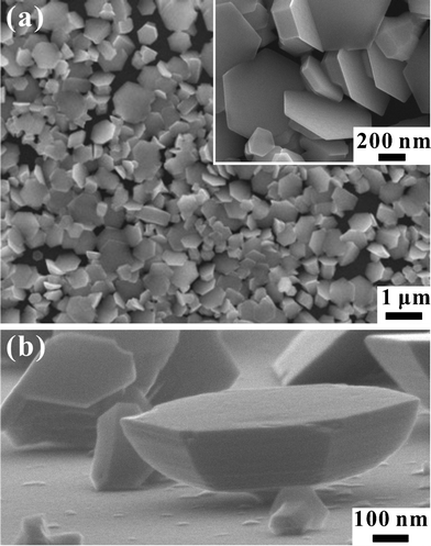 | ||
| Fig. 1 (a) FESEM images showing the top views of a large area array of 2D pure Zn-metal nanoplates on a Si substrate. (b) High-magnification FESEM image showing the side view (70° to the surface normal direction) of 2D pure Zn-metal nanoplates. | ||
Quantitative analyses of the electronic structures and chemical properties of the 2D pure Zn-metal nanoplates were performed using XPS. Fig. 2(a) illustrates the Zn 2p XPS spectra for the 2D pure Zn-metal nanoplates. The Zn 2p XPS spectra were decomposed using Voigt function fitting to precisely determine the features of the two peaks for Zn 2p3/2 and Zn 2p1/2. They are located at binding energies of 1022.0 and 1045.1 eV, respectively, and the energy separation between them is 23.1 eV. Note that the Zn 2p3/2 peaks at 1022.0 and 1023.0 eV represent pure Zn0 atoms and Zn2+ cations, respectively.29 The XPS results indicate that these 2D hexagonal nanoplates are composed of pure Zn metals only, including no zinc oxides (ZnO) at all. The XRD patterns are essentially the fingerprints of crystalline materials and can reveal details of the structure and the crystal growth formation during synthesis. Fig. 2(b) shows the XRD spectra and Rietveld refinement results for the 2D pure Zn-metal nanoplates. The diffraction peaks at 2θ = 36.3°, 39.1°, 43.2°, and 54.4° correspond respectively to the (002), (100), (101) and (102) lattice planes of the hexagonal Zn crystal in the space groupP63/mmc (JCPDS card no. 65-3358). The refined parameters are obtained for lattice constants of a = b = 2.66638 Å and c = 4.94881 Å, α = β = 90°, γ = 120°, χ2 = 1.901, Rp = 13.31% and Rwp = 20.64%, respectively.
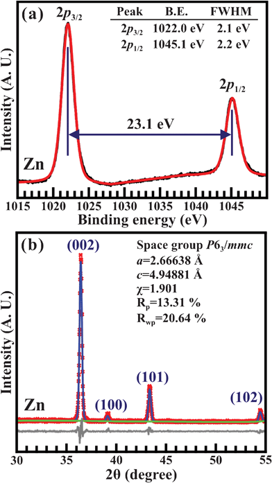 | ||
| Fig. 2 (a) XPS spectra of the Zn 2p3/2 and Zn 2p1/2 core levels of the 2D pure Zn-metal nanoplates. The XPS spectra are decomposed via Voigt function fitting. (b) XRD patterns and Rietveld refinement of the 2D pure Zn-metal nanoplates. | ||
Fig. 3(a) depicts the room-temperature PL spectra of the 2D pure Zn-metal nanoplates. The UV- and visible-light emissions can be clearly observed for a wide range of wavelengths from 312 to 700 nm. There are two main asymmetrical spectral bands centered at 400 and 458 nm, which correspond to the energy states of 3.1 ( E2) and 2.7 ( E3) eV. The shoulder band located at 362 nm corresponds to the energy state of 3.43 eV ( E1). Note that the wavelengths of 312, 500, 600 and 700 nm are reflected by the energies of 3.97, 2.48, 2.07 and 1.77 eV, respectively. As is commonly known, PL spectroscopy is a good optical method for probing the impurities, defects, and bandgaps in semiconductor materials. However, since the 2D pure Zn-metal nanoplates are comprised of only pure metallic Zn atoms, the PL emissions do not reflect the semiconductor properties alone. Fig. 3(b) shows a schematic representation based on Mooradian's model.1 The interband transitions are among the 3d (the region highlighted in yellow), sp-conduction bands and EF for metals at room-temperature. Electrons lying in the 3d band can be excited by an incident laser to move to the unoccupied levels of the sp-conduction band above the EF. The excited electrons then undergo nonradiative transitions to the EF. The electrons at the EF must drop back to the 3d band, so that room-temperature PL emissions of metals occur, releasing energy during the radiative transitions. In this study, the emitted UV and blue light emissions come from the factors so that the electrons at the EF drop to the upper levels (such as the E1 and E2 states) in the 3d band. However, the energy separation between the EF and the 3d band of the 2D pure Zn-metal nanoplates may be too large to generate the green, yellow and red light emissions. Mooradian's model cannot explain the occurrence of all PL emissions. We need to examine the valence-band and band-structure of the 2D pure Zn-metal nanoplates to further understand the occurrence of the green, yellow and red light emissions.
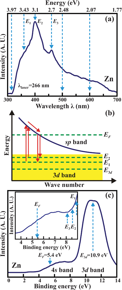 | ||
| Fig. 3 (a) Room-temperature PL spectra of the 2D pure Zn-metal nanoplates, where E1, E2, and E3 represent the energy states of 3.43, 3.1, and 2.7 eV, corresponding to 362, 400, and 458 nm, respectively. (b) Schematic representation of the excitation and recombination transition among the 3d (region highlighted in yellow), sp-conduction bands and EF. (c) The XPS spectra of the valence band, EF, 4s and 3d bands of the 2D pure Zn-metal nanoplates. | ||
Zn has an electronic configuration of [Ar]3d104s2. The outer 4s electrons easily become free electrons and are dispersed in a wide range of energies. The 3d electrons are tightly bound and relatively dispersed in a narrow range of energies. The XPS spectra in Fig. 3(c) show the valence band, EF, 4s and 3d bands of the 2D pure Zn-metal nanoplates. The 4s band has a small but broad peak, while the 3d band has a large peak. The EF is determined at the binding energy of 5.4 eV, and the 3d band peak is centered at 10.9 eV. Therefore, the EF–E3d energy separation between the EF and the center of the 3d band peak is 5.5 eV, which is much larger than the energy (= 4.66 eV) of the incident 266-nm laser. However, from the inset to Fig. 3(c), which displays the detailed electronic structure from the EF to the upper levels of the 3d band, it is evident that the E1 and E2 states lie at the tail of the 3d band. Actually, the E1 and E2 states are the upper levels of the 3d band, and the EF–E1 and EF–E2 energy separations are 3.4 and 3.2 eV, respectively. Hence, only the electrons in the upper levels of the 3d band can be excited to move to the sp conduction band, and the E1 and E2 states are able to provide the UV and blue light emissions. However, the E3 state does not lie in the tail. In other words, the E3 state is not on one of the upper levels, so it cannot provide any PL emissions. Therefore, we need to determine where the green, yellow and red light emissions come from.
Fig. 4 shows the calculated band structure of the 2D pure Zn-metal nanoplates. As can be seen in the inset to Fig. 4, the Brillouin zone is a 2D hexagonal reciprocal lattice. The 3d electrons lie in narrow bands (indicated by the green curves) around 5.5 eV with a high density of states, while the sp conduction bands (indicated by the blue curves) are relatively dispersed with a lower density of states. In the range from the K-point to the Γ-point, the energy separations between the EF and the upper levels of the 3d band are slightly smaller than the energy of the incident laser. Electrons in the upper levels of the 3d band are excited to the sp band, so some 3d–sp interband transitions (indicated by the red arrows) occur. The 3d–sp interband transitions can cause UV and blue light emissions, confirming the PL results shown in Fig. 3(a). However, in two ranges, from the Γ-point to the M-point and from the M-point to the K-point, the sp band is taken apart to form a bandgap, indicating that the 2D pure Zn-metal nanoplates also possess semiconducting characteristics. The bandgaps are ≤2.7 eV (= E3), so electrons in the valence band below the EF are easily excited from the valence band to the conduction band, the so-called valence–conduction interband transitions (indicated by the orange arrows). The excited electrons transit nonradiatively to the M-point, because the lowest valence level above the EF is located at the M-point. When the M-point electrons return to the valence band, they can emit the green, yellow and red light emissions (as shown in Fig. 3(a)), causing the release of energy during the radiative transitions. In addition, we found that the 2D pure Zn-metal nanoplates have both p- and n-type semiconducting properties in the range from the M-point to the Γ-point, and from the M-point to the K-point, respectively, suggesting that there is a p–n junction between these two ranges. Consequently, the 2D pure Zn-metal nanoplates not only demonstrate metallic, but also p- and n-type semiconducting characteristics, which give the 2D pure Zn-metal nanoplates excellent potential for use in optoelectronic nanodevices such as light-emitting diodes (LEDs) and solar cells.
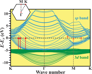 | ||
| Fig. 4 Calculated band structure of the 2D pure Zn-metal nanoplates. The red and orange arrows indicate the 3d–sp and valence–conduction interband transitions, respectively. The Brillouin zone of a 2D hexagonal reciprocal lattice is shown in the inset. | ||
D. Conclusions
The as-synthesized 2D pure Zn-metal nanoplates examined in this study were hexagonal crystals with an average width of ∼520 nm and thickness of ∼144 nm, and were possessed not only of metallic, but also semiconducting characteristics. In the metallic part, the EF of the 2D pure Zn-metal nanoplates was lowered close to the 3d core-level, so the EF–E3d energy separation is ∼5.5 eV, much smaller than that (∼10.2 eV) of bulk Zn metals. The small EF–E3d energy separation is the reason why the 2D pure Zn-metal nanoplates can provide UV and blue light emissions. In the semiconducting part, the sp band is taken apart to form a bandgap. The bandgap could let the 2D pure Zn-metal nanoplates emit the green, yellow, and red light.Acknowledgements
The authors would like to thank the National Science Council of the Republic of China for their financial support of this research under Contract Nos. NSC-99-2112-M-259-004-MY2, NSC-99-2738-M-259-001 and NSC-99-2811-M-259-008References
- A. Mooradian, Phys. Rev. Lett., 1969, 22, 185–187 CrossRef CAS.
- G. T. Boyd, Z. H. Yu and Y. R. Shen, Phys. Rev. B, 1986, 33, 7923–7936 CrossRef CAS.
- P. Apell, R. Monreal and S. Lundqvist, Phys. Scr., 1988, 38, 174–179 CrossRef CAS.
- S. S. Chang, S. O. Yoon, H. J. Park and A. Sakai, Appl. Surf. Sci., 2000, 158, 330–334 CrossRef CAS.
- S.-S. Chang, S. O. Yoon, H. J. Park and A. Sakai, Mater. Lett., 2002, 53, 432–436 CrossRef CAS.
- M. E. Stora and R. E. Hummel, J. Phys. Chem. Solids, 2002, 63, 1867–1872 CrossRef CAS.
- Y. Tong, M. Shao, G. Qian and Y. Ni, Nanotechnology, 2005, 16, 2512–2515 CrossRef CAS.
- A. V. Maciel, A. E. Job, W. D. Mussel, W. de Brito and V. M. D. Pasa, Biomass Bioenergy, 2011, 35, 1121–1129 CrossRef CAS.
- L. Kumari, S.-J. Lin, J.-H. Lin, Y.-R. Ma, P.-C. Lee and Y. Liou, Appl. Surf. Sci., 2007, 253, 5931–5938 CrossRef CAS.
- L. Kumari, J.-H. Lin and Y.-R. Ma, J. Phys. D: Appl. Phys., 2008, 41, 025405 CrossRef.
- Y.-R. Ma, C.-M. Lin, C.-L. Yeh and R.-T. Huang, J. Vac. Sci. Technol., B, 2005, 23, 2141–2145 CAS.
- L. Kumari, Y.-R. Ma, C.-C. Tsai, Y.-W. Lin, S. Y. Wu, K.-W. Cheng and Y. Liou, Nanotechnology, 2007, 18, 115717 CrossRef.
- L. Kumari, J.-H. Lin and Y.-R. Ma, Nanotechnology, 2007, 18, 295605 CrossRef.
- L. Kumari, J.-H. Lin and Y.-R. Ma, J. Phys.: Condens. Matter, 2007, 19, 406204 CrossRef.
- R. S. Devan, W.-D. Ho, J.-H. Lin, S. Y. Wu, Y.-R. Ma, P.-C. Lee and Y. Liou, Cryst. Growth Des., 2008, 8, 4465–4468 CAS.
- R. S. Devan, W.-D. Ho, C.-H. Chen, H.-W. Shiu, C.-H. Ho, C.-L. Cheng, S. Y. Wu, Y. Liou and Y.-R. Ma, Nanotechnology, 2009, 20, 445708 CrossRef.
- R. S. Devan, W.-D. Ho, S. Y. Wu and Y.-R. Ma, J. Appl. Crystallogr., 2010, 43, 498–503 CrossRef CAS.
- R. S. Devan, J.-H. Lin, W.-D. Ho, S. Y. Wu and Y.-R. Ma, J. Appl. Crystallogr., 2010, 43, 1062–1067 CrossRef CAS.
- R. S. Devan, S.-Y. Gao, W.-D. Ho, J.-H. Lin, Y.-R. Ma, P. S. Patil and Y. Liou, Appl. Phys. Lett., 2011, 98, 133117 CrossRef.
- R. S. Devan, C.-L. Lin, S.-Y. Gao, C.-L. Cheng, Y. Liou and Y.-R. Ma, Phys. Chem. Chem. Phys., 2011, 13, 13441–13446 RSC.
- R. Jin, Y. W. Cao, C. A. Mirkin, K. L. Kelly, G. C. Schatz and J. G. Zheng, Science, 2001, 294, 1901–1903 CrossRef CAS.
- R. Jin, Y. C. Cao, E. Hao, G. S. Métraux, G. C. Schatz and C. A. Mirkin, Nature, 2003, 425, 487–490 CrossRef CAS.
- Y. Xiong, J. M. McLellan, J. Chen, Y. Yin, Z.-Y. Li and Y. Xia, J. Am. Chem. Soc., 2005, 127, 17118–17127 CrossRef CAS.
- R. S. Devan, J.-H. Lin, Y.-J. Huang, C.-C. Yang, S. Y. Wu, Y. Liou and Y.-R. Ma, Nanoscale, 2011, 3, 4339–4345 RSC.
- N. S. Azmat, K. D. Ralston and I. S. Cole, Surf. Coat. Technol., 2010, 205, 928–935 CrossRef CAS.
- L. Ley, S. P. Kowalczyk, F. R. McFeely, R. A. Pollak and D. A. Shirley, Phys. Rev. B, 1973, 8, 2392–2402 CrossRef CAS.
- P. Hohenberg and W. Kohn, Phys. Rev., 1964, 136, B864–B871 CrossRef.
- W. Kohn and L. J. Sham, Phys. Rev., 1965, 140, A1133–A1138 CrossRef.
- D. Pradhan, S. Sindhwani and K. T. Leung, J. Phys. Chem. C, 2009, 113, 15788–15791 CAS.
| This journal is © The Royal Society of Chemistry 2012 |