Ag2Se micropatterns via viscoelastic flow-driven phase separation†
Minwoo
Park
a,
Heesook
Cho
b,
Soojin
Park
b and
Unyong
Jeong
*a
aDepartment of Materials Science and Engineering, Yonsei University, 134 Shinchon-dong, Seoul, Korea. E-mail: ujeong@yonsei.ac.kr
bInterdisciplinary School of Green Energy, UNIST, 689-798, Ulsan, Korea
First published on 29th March 2012
Abstract
A novel approach to prepare micropatterns of metal chalcogenides is proposed by employing viscoelastic flow-driven patterning. A consecutive process involving deposition of the Se precursor on a pattern of a crystalline polymer, chemical reduction of the precursor into amorphous Se (a-Se), and short-time thermal annealing above the melting temperature of the patterned polymer generated regular patterns of a-Se. This work demonstrates patterns of periodic lines and circles which is driven by the viscoelastic polymer flow and the phase separation of Se from the polymer. Additional thermal annealing facilitated the lateral growth of trigonal-Se (t-Se) nanowires from the Se patterns. The growing t-Se nanowires eventually meet each other to produce a 2D network structure. Chemical transformation of the Se into Ag2Se generated metal chalcogenide network structures.
Introduction
Metal chalcogenides have attracted considerable research interest for many decades due to their unique semiconducting, thermal and optical properties which are useful for the fabrication of photovoltaic devices, light detection, light emitting, thermoelectric devices, ultrasonic transducers and electrostatic imaging devices.1–4 The performance and application of the materials not only depend on the chemical composition, but also strongly depend on the approach to prepare the patterns of the metal chalcogenides. Electrodeposition followed by selective etching has been employed to obtain micro-patterns typically larger than μm.5 Evaporation through a mask also has been attempted to generate chalcogenide patterns.6 Some groups adapted directed self-assembly of chalcogenide nanowires to prepare aligned structures on patterned substrates.7–9In this paper, we suggest a novel approach to prepare micropatterns of metal chalcogenides. We employed viscoelastic flow-driven patterning which allows patterning of diverse inorganic materials including metals and semiconductors.10 The Se precursors were deposited on a pattern of a crystalline polymer obtained from capillary force lithography (CFL), which is a soft lithography producing polymer patterns by the capillary effect in the channels of a rubbery stamp. The stamp is placed on a polymer layer and thermal annealing is applied to induce polymer flow.11 Subsequently the Se precursors are reduced into amorphous Se (a-Se) nanoparticles. Simple thermal annealing above the melting point of the patterned polymer leads to polymeric flow to the recessed regions in the polymer pattern. The Se nanoparticles were phase-separated from the polymer flow and concentrated at the center of the recessed regions, forming a regular pattern of continuous a-Se lines. The a-Se lines were chemically transformed into Ag2Se.12 It was proven that the Ag2Se can be further transformed into diverse metal chalcogenides such as CdSe, Bi2Se3, PbSe, ZnSe, etc.13–21 Additional thermal annealing facilitated the lateral growth of trigonal (t-Se) nanowires from the Se lines. The growing t-Se nanowires eventually meet each other to produce a network structure. Transformation of the t-Se nanowires converted the Se network into an Ag2Se network, and further into other metal chalcogenides.
Experimental
Materials
Poly(ε-caprolactone) (PCL) (Mn = 42![[thin space (1/6-em)]](https://www.rsc.org/images/entities/char_2009.gif) 500), silver nitrate (AgNO3 99.9999%, metal basis), hydrazine hydrate (reagent grade, N2H4 50–60%) and selenious acid (H2SeO3 98%) were purchased from Sigma Aldrich. The Sylgard 184 elastomer kit was purchased from Dow Corning to make PDMS molds (line/space = 1.55 μm/1.55 μm). Ethylene glycol (99.9%), ethanol (94.9%), methanol (99.9%), toluene (99.9%) and trichloroethylene (99.5%) were purchased from J. T. Baker. The silicon wafers were cleaned with trichloroethylene and methanol under ultrasonic conditions for 10 min, followed by rinsing with pure DI water (18.2 MΩ) and drying with nitrogen gas. PDMS molds from a Si-wafer master pattern were prepared by thermal curing at 60 °C for 12 h.
500), silver nitrate (AgNO3 99.9999%, metal basis), hydrazine hydrate (reagent grade, N2H4 50–60%) and selenious acid (H2SeO3 98%) were purchased from Sigma Aldrich. The Sylgard 184 elastomer kit was purchased from Dow Corning to make PDMS molds (line/space = 1.55 μm/1.55 μm). Ethylene glycol (99.9%), ethanol (94.9%), methanol (99.9%), toluene (99.9%) and trichloroethylene (99.5%) were purchased from J. T. Baker. The silicon wafers were cleaned with trichloroethylene and methanol under ultrasonic conditions for 10 min, followed by rinsing with pure DI water (18.2 MΩ) and drying with nitrogen gas. PDMS molds from a Si-wafer master pattern were prepared by thermal curing at 60 °C for 12 h.
Fabrication of the PCL line patterns
PCL line patterns were made by capillary force lithography (CFL). After spin-coating a PCL solution (6 wt% in toluene) on a cleaned wafer at 3000 rpm for 30 sec, a PDMS mold was placed on the PCL film (382 nm thickness). The samples were annealed at 80 °C for 5 min and cooled to room temperature in air. The PDMS mold was slowly lifted off the substrate. The line-and-space dimension of the PCL pattern was 1.55 μm/1.55 μm, and the average height of the polymer lines was 940 nm (see Fig. S1, ESI†).Fabrication of the a-Se line patterns
The PCL pattern was treated with oxygen plasma (60 W, 22 SCCM, 40 s). A small amount of H2SeO3 ethanol solution (0.03 ml, 20 mM) was dropped on the PCL pattern. The solution immediately spread on the PCL pattern. After drying at room temperature in the air, the pattern was exposed to N2H4 vapor for 3 min in a beaker to reduce the Se precursor into a-Se particles. The specimen was annealed at 90 °C for 30 min in a heating block. The viscous flow produced regularly-spaced a-Se lines. Additional annealing at 90 °C for 6 h crystallized the a-Se and produced t-Se nanowires laterally grown from the a-Se lines.Chemical transformation of Se into Ag2Se
AgNO3 was dissolved in ethylene glycol (0.1 M). The a-Se pattern was soaked in the Ag precursor solution at room temperature. The reaction time required for the transformation was dependent on the thickness and width of the a-Se lines. The degree of transformation was controlled by the soaking time (0.5–26 h). The transformation of the t-Se nanowires into Ag2Se was completed within 10 min. After chemical transformation, the sample was thoroughly rinsed with DI water several times to remove the residual Ag precursors. The PCL pattern was selectively removed by dissolving in chloroform to leave a line pattern of Ag2Se.Characterization
The morphologies were investigated with field emission scanning electron microscopy (FE-SEM, JSM-7001F, JEOL Co.). The dimension of the patterns was measured with atomic force microscopy (AFM, Dimension 3100, Digital Instrument Co.). To analyze the cross-sectional distribution of Ag and Se after the chemical transformation, the Ag2Se line patterns on a Si wafer were molded in epoxy (EpoFix-Kit) and cured for 12 h at room temperature. The patterns were cleanly detached from the Si-wafer and embedded in epoxy. They were cut by a microtoming machine (PowerTome PC, SIMS Co., Ltd.) into 100 nm-thick films. The mapping was conducted with HR-TEM equipped with EDX (JEOL 2100F). The I–V characteristics were measured with an Agilent 4156 A.Results and discussion
The process in this study involves fabrication of a line pattern of amorphous selenium (a-Se) and chemical transformation the a-Se into trigonal selenium (t-Se) or silver selenide (Ag2Se). Fig. 1 shows the overall process for the in-situ formation of a-Se lines and their chemical transformation into Ag2Se. One droplet of Se precursor solution in ethanol was dropped on a line pattern of PCL prepared by CFL. The polymer pattern was treated with oxygen plasma to enhance the spreading of the precursor solution.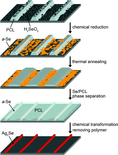 | ||
| Fig. 1 Schematic illustration for the viscoelastic flow of poly(ε-carprolactone) (PCL) melt and the phase separation between a-Se and PCL. The process generates a line pattern of a-Se. The Se precursors (H2SeO3) were randomly deposited on the line-and-space pattern of PCL and chemically reduced into amorphous selenium (a-Se). The viscoelastic flow of the PCL melt was triggered by thermal annealing at above the melting temperature of PCL (60 °C). The melt flow collected the a-Se at the trenches. The a-Se lines were chemically transformed into Ag2Se. | ||
The precursor solution uniformly spread out over the whole PCL pattern. A large fraction of the precursor was selectively precipitated in the recessed region due to the capillary effect during solvent evaporation.24 Chemical reduction produced a large number of amorphous Se (a-Se) particles randomly scattered on the PCL layers. On heating at 90 °C which is higher than the melting temperature of PCL (∼60 °C) and glass transition temperature of a-Se (∼32 °C), the PCL liquid flowed toward the recessed regions. Due to the large interfacial tension (γ) between a-Se and the PCL liquid (121.3 ± 20 mN m−1), the a-Se particles were phase-separated from the PCL liquid so that they were concentrated in the PCL-free recessed regions. The interfacial tension between a-Se and PCL was calculated by Young's equation:
| γSe-PCL = γSe − γPCLcosθ |
The a-Se liquid particles quickly merged with each other and formed continuous lines. As the PCL liquid pushes the Se lines from both sides, the interface became sharp, and narrow a-Se lines were generated. On cooling to room temperature, the crystallization of PCL started from the interface with the Se lines and propagated to the perpendicular direction to the line patterns. The a-Se lines were chemically transformed into Ag2Se by dipping the pattern in a Ag precursor solution in ethylene glycol at 50 °C. The reduced Ag atoms by the ethylene glycol solvent immediately reacted with a-Se atoms to form an alloy.
In the process described above, the use of crystalline polymer was essential. The rapid drop of the viscosity above the melting temperature (Tm) of crystalline polymers enabled polymeric flow and provided a-Se liquid particles with high mobility.10 During the CFL patterning process, the use of crystalline polymer could minimize possible residual layers on the substrate.10,25
Fig. 2 shows FE-SEM images corresponding to the serial process of the in-situ formation of the a-Se lines. After dropping the H2SeO3 solution, the small precipitates of the precursor were evenly scattered on the PCL pattern (Fig. 2A). Chemical reduction by hydrazine (N2H4) vapor in a closed chamber immediately generated a-Se particles and lumps randomly scattered on the PCL pattern (Fig. 2B).26 The hydrazine vapor did not damage the molecular structure of PCL chains.10 Large amounts of a-Se were located in the recessed regions of PCL pattern but a-Se particles were also found on the walls and tops of the PCL lines. On annealing at 90 °C, the a-Se particles immediately merged to form continuous lines. After 30 min annealing, the sample was cooled to room temperature in air. PCL crystals grew from the wall of the a-Se lines (Fig. 2C). The inset shows the EDX mapping, clearly verifying the phase separation between a-Se and PCL in the step of Fig. 2C (also see Fig. S2, ESI†). After selectively removing the PCL pattern by chloroform, well-aligned a-Se lines were obtained (Fig. 2D). The average diameter and height of the pattern were 600 and 420 nm, respectively (see Fig. S3, ESI†).
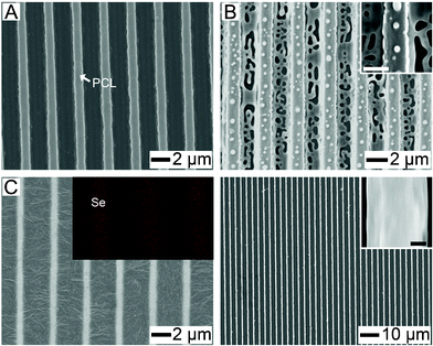 | ||
| Fig. 2 SEM images represent the serial process for the formation of a-Se lines. (A) SEM image obtained after deposition of H2SeO3 by spraying its ethanol solution on the PCL pattern. (B) The generation of a-Se particles on the whole PCL surface after chemical reduction. The scale-bar of the inset is 1.5 μm. (C) The formation of the a-Se line pattern after thermal annealing (90 °C). (D) Periodic a-Se lines were obtained by dissolving out PCL. The scale-bar of the inset is 150 nm. | ||
The chemical transformation of chalcogens (Se, Te) into various metal chalcogenides has been well demonstrated in nanoparticles, mesoscale particles and nanowires.13–15 Xia and co-workers reported that chalcogen nanowires can be directly transformed into various metal chalcogenides by simply reacting the chalcogen nanowires in solutions of metal precursors.16–18 We demonstrated that silver chalcogenides can be further transformed into other metal chalcogenides such as CdTe, PbTe, ZnTe, Bi2Te3 and PtTe2.18–21 Because this transformation can largely diversify the species of the metal chalcogenide materials, starting with patterned chalcogens may produce various metal chalcogenide patterns. Fig. 3 shows the cross-sectional TEM images of the Se lines after scheduled times of chemical transformation into Ag2Se. Ethylene glycol acted as a weak reducing agent for the Ag+ ions. The reduced Ag0 atoms diffused in the a-Se and generated Ag2Se alloy. Because we used pure EG in this study, silver selenate impurities were not produced, as happens in the presence of water. The transformation at the surface area immediately proceeded and the conversion slowed down due to the reduced diffusion rate into the sub-micron thick a-Se lines. Even when the Ag nanoparticles are generated in the solution, they cannot diffuse through the Ag2Se barrier. Fig. 3A exhibits a cross-sectional dark-field TEM image of the a-Se line after 30 min transformation. The atomic composition profiles of Ag and Se along the lines in the TEM image are shown. The average composition along the entire thickness was Ag:Se = 0.34:1. The outer surfaces were Ag-rich, while most inner regions were still Se (Fig. 3A). The brighter layer indicated by arrows in Fig. 3A was identified as Ag2Se. Selective dissolution of the unreacted a-Se by soaking in a toluene-based trioctylphosphine solution (1%, v/v) produced Ag2Se shells (Fig. 3B). Fig. 3C shows a bright-field TEM image of a piece of the hollow Ag2Se shell. The thickness of the shell was 40 nm. The selected area (marked a circle in Fig. 3C) electron diffraction (SAED) of the fragment clearly demonstrated that the transformed shells had the orthorhombic crystal structure of polycrystalline Ag2Se (Fig. 3D). The results indicate that the transformation gradually took place from the surface or interface with the hydrophilic SiO2 layer.
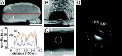 | ||
| Fig. 3 (A) Cross-sectional dark-field STEM image of a Ag2Se line imperfectly transformed from a a-Se line. The transformation reaction time was 30 min. The white arrows indicate the transformed Ag2Se. The elemental profile along the line in the STEM image is also shown. (B) Cross-sectional SEM image of (A) obtained after dissolving the unreacted Se. (C) Bright field TEM image for a fragment of the Ag2Se shell of (B). The white arrows indicate the 40 nm-thick Ag2Se shell. (D) Selected area electron diffraction (SAED) from a circle in (C). | ||
After 26 h chemical transformation, the a-Se lines were completely transformed into Ag2Se, as shown in Fig. 4A. The average chemical composition of Ag and Se was 2:1 and the local composition was the same at any position. The transformation from the a-Se pattern into the Ag2Se pattern increased the volume by ∼60%, increasing the line thickness from 420 ± 30 nm to 480 ± 20 nm and the line width from 500 ± 20 nm to 790 ± 20 nm. The average values were taken from 100 measurements at different locations of 10 samples. The increase in the line width was the main contribution to the increase in the total volume and is attributed to the high compatibility of Se to the neighboring PCL lines.27 Se atoms are known to be soluble in organic solvents containing ether and carbonyl groups. Therefore, the material flux of Se toward the PCL lines followed by chemical transformation was the main reason for the larger increase in the line width rather than in the line thickness. The measured volume increase was smaller than the calculated value (ΔV ∼ 90%) and is caused by the partial dissolution of Se which was not used in the chemical transformation from the Se lines. Normally, large volume increase causes stress-induced breaking or delamination. Without PCL thin films, the lines were broken (Fig, S4, ESI†), and it is thought that the neighboring PCL lines fixed the a-Se lines to the substrate so that volume change took place in the thickness direction. The transformed Ag2Se was of orthorhombic structure. The high-resolution TEM image of a cross-sectioned Ag2Se line clearly demonstrates the orthorhombic lattice of β-Ag2Se (Fig. 4B).
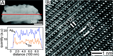 | ||
| Fig. 4 (A) Cross-sectional dark-field STEM image of a Ag2Se line transformed from a a-Se line. The transformation reaction time was 26 h. The inset graph indicates the elemental profile of along the red line. (B) High-resolution TEM image of (A). | ||
The electrical conductivity of the Ag2Se was largely dependent on the extent of transformation. Fig. 5A shows a SEM image of an array of Ag2Se lines bridging two rectangular Au electrodes on an undoped-Si wafer. In order to minimize the height deviation between the oxide layer (200 nm) and the Au electrodes, the Au electrodes were embedded in trenches of the oxide layer. The a-Se lines were prepared on the Au-incorporating Si wafer and they were transformed into the Ag2Se lines following the same procedure mentioned above. The gap between the electrodes was 100 μm and the width of each electrode was 200 μm. Fig. 5B shows the I–V characteristics for the Ag2Se lines. Transformation for 30 min (line 1) gave a low conductivity (6.0 × 10⁻¹ S/m). The conductivity slowly increased as the reaction time was raised. Lines 2 and 3 indicate the results after transformation for 2 and 8 h, respectively. After 15 h transformation (line 4), the conductivity increased substantially and showed ohmic behavior in the entire voltage range. Transformation for 26 h (line 5) led to highly conductive Ag2Se (5.8 × 10⁵ S m−1) which is more conductive than for single-crystal Ag2Se nanowires (8.3 × 10⁴ S m−1 at room temperature) prepared in a solution process.28 The high conductivity of the multi-grained lines infers heavy doping of Ag in the Ag2Se. The possible presence of Ag nanoparticles at the surface of the transformed Ag2Se lines also cannot be completely discounted, which may give an extra contribution to the enhanced conductivity. Unfortunately, the precise identification of the particles was not possible.
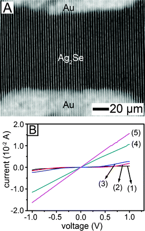 | ||
| Fig. 5 (A) SEM image of a Ag2Se line pattern directly created between two Au electrodes. (B) I–V characteristics as a function of transformation time from a-Se into Ag2Se: (1) 30 min, (2) 2 h, (3) 8 h, (4) 15 h and (5) 26 h. | ||
Thermal annealing of the a-Se allowed growth of the t-Se nanowires at the surface. Previously, we reported the growth mechanism of the t-Se nanowires from a-Se particles embedded in compatible polymer thin films.27 The growth of the t-Se was confined in the polymer layer. The growth rate was much faster than the vapor-phase growth. In this study, the nucleation of t-Se took place at the interface with the PCL on annealing at 90 °C. The t-Se nanowires grew in the PCL melt and touched the neighboring Se lines, generating a two-dimensional (2D) network of Se and this network formation was complete within 6 h. Fig. 6A and B demonstrate the Se networks created from parallel lines (Fig. 6A) and regular circles (Fig. 6B). The circular Se pattern was prepared via CFL with a PDMS stamp having regular cylindrical pillars. The diameter of the Se rings was 10 μm. The thickness of the t-Se nanowires emerging from the Se lines ranged from 30 to 50 nm (Fig. S5, ESI†). They have many interconnections as seen in the insets of Fig. 6A and B. Chemical transformation produced an inter-connected structure of Ag2Se (Fig. 6C and D). The structure and junctions were preserved after the chemical transformation. The transformed Ag2Se nanowires also had orthorhombic structure (Fig. S6, ESI†). The interconnection of the Ag2Se nanowires could be checked via I–V characteristics in the perpendicular direction to the Se lines and rings (as depicted in Fig. 6E and F). The conductivity of the transformed Ag2Se networks was 31 S m−1 which was compatible to the conductivity through the line pattern after 8 h reaction conversion (line 3 in Fig. 5B).
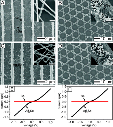 | ||
| Fig. 6 (A, B) SEM images of t-Se nanowire networks between the a-Se lines and the rings, respectively. The blow-up images of (A) and (B) visualize the contact between the t-Se nanowires. The scale-bar of the inset in (A) is 100 nm and in (B) is 500 nm. (C, D) SEM images obtained after chemical transformation of (A) and (B) into Ag2Se, respectively. The blow-up images of (C) and (D) represent the Ag2Se nanowire network. The scale-bar of the inset in (C) is 200 nm and in (D) is 1 μm. (E, F) I–V characteristics of the t-Se and Ag2Se networks. For (E), the measurement was carried out in the perpendicular direction to the regular Ag2Se lines. | ||
Conclusion
In this study, we demonstrated the in-situ patterning in micro-scale of a-Se and its chemical transformation into β-Ag2Se. At above the melting temperature of PCL, the flow of the PCL liquid pushed the a-Se on the PCL pattern. The Se particles were phase-separated and collected in the recessed area of the polymer pattern. The a-Se patterns were successfully transformed into the patterns of orthorhombic Ag2Se. The conductivity changed from a semiconductor to a conductor by adjusting the degree of transformation. Additional thermal annealing of the a-Se patterns led to perpendicular growth of the t-Se nanowires from the patterns to lead to a 2D network, which could serve as a template for a 2D Ag2Se network.Acknowledgements
This research was partly supported by the National Research Foundation (NRF) grant funded by the Korean Government (MEST) through the Active Polymer Center Pattern Integration (No. R11-2007-050-01004-0), the World Class University Program (R32-20031), and Fusion Research Program for Green Technologies (2011-0000004).References
- W. U. Huynh, J. J. Dittmer and A. P. Alivisatos, Science, 2002, 295, 2425 CrossRef CAS.
- J. Ham, W. Shim, D. H. Kim, S. Lee, J. Roh, S. W. Sohn, K. H. Oh, P.W. Voorhees and W. Lee, Nano Lett., 2009, 9, 2867 CrossRef CAS.
- M. Lee, T. F. Rosenbaum, M.-L. Saboungi and H. S. Schnyders, Phys. Rev. Lett., 2002, 88, 066602 CrossRef CAS.
- I. L. Medintz, H. T. Uyeda, E. R. Goldman and H. Mattoussi, Nat. Mater., 2005, 4, 435 CrossRef CAS.
- I. B. Divliansky, A. Shishido, I.-C. Khoo, T. S. Mayer and D. Pena, Appl. Phys. Lett., 2001, 79, 3392 CrossRef CAS.
- V. Takáts, F. C. Miller, H. Jain, C. Cserháti, I. A. Szabó, D. Beke and S. Kokenyesi, J. Non-Cryst. Solids, 2009, 355, 1849 CrossRef.
- J.-W. Liu, J.-H. Zhu, C.-L. Zhang, H.-W. Liang and S.-H. Yu, J. Am. Chem. Soc., 2010, 132, 8945 CrossRef CAS.
- B. T. Mayers, K. Liu, D. Sunderland and Y. Xia, Chem. Mater., 2003, 15, 3852 CrossRef CAS.
- R. Ma, Y. Wang and T. E. Mallouk, Small, 2009, 5, 356 CrossRef CAS.
- M. Park, Y. Xia and U. Jeong, Angew. Chem., Int. Ed., 2011, 50, 10977 CrossRef CAS.
- K. Y. Suh, Y. S. Kim and H. H. Lee, Adv. Mater., 2001, 13, 1386 CrossRef CAS.
- U. Jeong and Y. Xia, Angew. Chem., Int. Ed., 2005, 44, 3099 CrossRef CAS.
- D. H. Son, S. M. Hughes, Y. Yin and A. P. Alivisatos, Science, 2004, 306, 1009 CrossRef CAS.
- A. Dorn, P. M. Allen, D. K. Harris and M. G. Bawendi, Nano Lett., 2010, 10, 3948 CrossRef CAS.
- G. D. Moon, S. Ko, Y. Min, J. Zeng, Y. Xia and U. Jeong, Nano Today, 2011, 6, 186 CrossRef CAS.
- U. Jeong, P. H. C. Camargo, Y. H. Lee and Y. Xia, J. Mater. Chem., 2006, 16, 3893 RSC.
- X. Jiang, B. Mayers, T. Herricks and Y. Xia, Adv. Mater., 2003, 15, 1740 CrossRef CAS.
- B. Gates, B. Mayers, Y. Wu, Y. Sun, B. Cattle, P. Yang and Y. Xia, Adv. Funct. Mater., 2002, 12, 679 CrossRef CAS.
- P. C. Carmago, Y. H. Lee, U. Jeong, Z. Zhou and Y. Xia, Langmuir, 2007, 23, 2985 CrossRef.
- U. Jeong and Y. Xia, Chem. Phys. Lett., 2005, 416, 246 CrossRef CAS.
- G. D. Moon, S. Ko, Y. Xia and U. Jeong, ACS Nano, 2010, 4, 2307 CrossRef CAS.
- L. B. Harris and J. P. Vernon, J. Polym. Sci., Part A-2, 1972, 10, 499 CrossRef CAS.
- D. Cava, R. Gavara, J. M. Lagaron and A. Voelkel, J. Chromatogr., A, 2007, 1148, 86 CrossRef CAS.
- D. C. Hyun, M. Park, C. Park, B. Kim, Y. Xia, J. H. Hur, J. M. Kim, J. J. Park and U. Jeong, Adv. Mater., 2011, 23, 2946 CrossRef CAS.
- M. Park, D. C. Hyun, J. Kim, Y. Kim and U. Jeong, Chem. Mater., 2010, 22, 2642 Search PubMed.
- B. Gates, Y. Yin and Y. Xia, J. Am. Chem. Soc., 2001, 123, 11500 CrossRef CAS.
- S. Ko, M. Park, J. S. Lee, Y. S. Kim, D. Y. Ryu and U. Jeong, Chem. Commun., 2009, 1855 RSC.
- D. T. Schoen, C. Xie and Y. Cui, J. Am. Chem. Soc., 2007, 129, 4116 CrossRef CAS.
Footnote |
| † Electronic supplementary information (ESI) available: AFM images of PCL and a-Se line pattern, SEM-EDX mapping for the phase separation between a-Se and PCL, SEM image of broken Ag2Se upon chemical transformation, TEM images of t-Se and Ag2Se nanowires detached from a-Se and Ag2Se lines, respectively. See DOI: 10.1039/c2ra00024e |
| This journal is © The Royal Society of Chemistry 2012 |