Dual-color electrochromic films incorporating a periodic polymer nanostructure
Hung-Yu
Wei
a,
Yu-Sheng
Hsiao
b,
Jen-Hsien
Huang
b,
Chih-Yu
Hsu
c,
Feng-Chih
Chang
d,
Peilin
Chen
b,
Kuo-Chuan
Ho
*ac and
Chih-Wei
Chu
*be
aInstitute of Polymer Science and Engineering, National Taiwan University, Taipei, 10617, Taiwan
bResearch Center for Applied Sciences, Academia Sinica, Taipei, 11529, Taiwan. E-mail: gchu@gate.sinica.edu.tw
cDepartment of Chemical Engineering, National Taiwan University, Taipei, 10617, Taiwan. E-mail: kcho@ntu.edu.tw
dDepartment of Applied Chemistry, National Chao Tung University, Hsinchu, 30010, Taiwan
eDepartment of Photonics, National Chiao Tung University, Hsinchu, 300, Taiwan. E-mail: gchu@gate.sinica.edu.tw
First published on 13th March 2012
Abstract
In this study, we used electrochemical deposition with a polystyrene (PS) bead template to prepare thin layers of poly(3,4-ethylenedioxythiophene) (PEDOT) that has a nanometer-scale honeycomb periodicity. To achieve dual-color electrochromic films, we then used pulsed electrochemical deposition to form polyaniline (PANI) layers on the rims of the PEDOT honeycomb film. Modifying the depositing charge density of PANI allowed tuning of the color of the composite films. We estimated the coloration efficiencies with respect to the values expected for corresponding amounts of pristine single layers of PEDOT and PANI. As a result of improved contact between the polymer film and the electrolyte, the coloration efficiencies of the structured composite films were much closer to their theoretical values than those of the corresponding bilayer composite films. Moreover, the switching times of the structured composite films were much faster than those of the bilayer composite films prepared without the nanostructures.
1. Introduction
Electrochromic materials continue to attract attention because of their applications in systems such as smart windows, anti-glare rear-view mirrors, sunglasses, and electrochromic displays.1–6 Conducting polymers are one family of electrochromic materials that possess the advantageous features of ready color tuning, high transmittance attenuation, rapid optical response, high coloration efficiency, and environmental stability. Among the conducting polymers, poly(3,4-ethylenedioxythiophene) (PEDOT) and polyaniline (PANI) have been studied extensively because of their low oxidation potentials and increased stability in the doped form at ambient and elevated temperatures. As a result, electrochromic devices based on thin films of PEDOT and PANI have attracted considerable attention from academic research groups. PEDOT switches from its oxidized transparent light blue form to its reduced dark blue form; PANI switches from its oxidized dark green form to its reduced transparent yellow form.7 Traditionally, complementary electrochromic devices have been prepared using a cathodically colored material (e.g., PEDOT) on one electrode and an anodically colored material (e.g., PANI) on another.5,8 This strategy causes each electrode to turn dark at the same time upon reduction of the PEDOT film (oxidation of PANI) and to bleach at the same time upon oxidation of PEDOT (reduction of PANI). In such devices, it is not possible to see a blue or green film in the colored state because the absorption spectra of both materials are added together to ensure the wide-range absorption of visible light. This property is good for smart windows, but not for electrochromic displays. A display featuring only bleached and darkened states would not be acceptable in today's world. Several attempts have been made to fabricate bilayer or multilayer electrochromic films in the quest for more colorful electrochromic displays.9–11Bilayer (or multilayer) electrochromic films have the inherent serious problem of the electrolyte not coming into direct contact with the bottom layers. The oxidation and reduction processes of the electrochromic materials rely on charge transfer with the electrolyte. If the bottom layer does not come into contact with the electrolyte, the electrochromic behavior would be restricted. Both physical and chemical methods have been developed to solve this problem. For physical methods, T. Brezesinski et al. and S. L. Kuai et al. both created a mesoporous WO3 thin film to improve the penetration of electrolytes into the inorganic framework, resulting in faster switching times and enhanced switching stability.12,13 Xia et al. proposed a facile method for producing periodic bowl-like cobalt oxide (Co3O4) array films to ensure improved electrochromic behavior by providing shorter diffusion pathways for the ions as well as a larger active surface area.14 Applied on conductive polymers, Bartlett et al. and Yang et al. also proved that they can create a film with 2 dimensional or 3 dimensional structure through templating and electrodeposition procedures and dramatically increased the surface area of the conducting polymer film.15,16 These reports reveal that the presence of a structured electrochromic layer can improve the contact between electrochromic material and electrolyte dramatically. Electrolyte diffusion is not a dominant problem in single-layer electrochromic thin films, but it is a serious one in bilayer electrochromic systems. Unfortunately, WO3 is not a good first-layer candidate for bilayer or multilayer electrochromic films because it is difficult to electrodeposit other materials onto WO3 as a second layer. Using a chemical method, Jia et al. designed a star-like PANI derivative to form an electrochromic film that had a porous morphology, thereby improving the diffusion of the electrolyte, increasing the electrochromic contrast, and shortening the switching time.17 The drawback of this approach, however, is that it improves ion transfer only for a single material, even if it is in the form of a multilayer thin film. If we wish to stack different materials in a multilayered electrochromic device, we would have to design another star-like molecule to ensure efficient ion transportation; such investigations would be expensive and time-consuming.
Electrochemical methods can be used to control film morphologies merely by changing the deposition conditions (e.g., applied voltage, duration time, cyclic voltammetry, pulse deposition). In 2008, Ratcliff et al. claimed that the use of a pulsed deposition protocol could lead to textured polymer films as a result of termination of film growth after a brief nucleation event. During the pulse in the “current on” stage, deposition occurred; during the “current off” stage, deposition ceased, allowing the monomers time to diffuse back to the film–liquid surface and refill the original diffusion layer region.18 With this technique, Ratcliff et al. created a carpet-like P3HT layer that could form an interpenetrating active layer and used it to fabricate a high-efficiency photovoltaic devices. Based on the same mechanism, in this study, we developed a simple approach, combining physical and electrochemical strategies, to stack different materials while retaining good ion transport properties. Using polystyrene (PS) beads as a template, we created a bowl-like structured PEDOT layer and then employed pulsed electrochemical deposition to polymerize PANI on the rim of the bowl-like structured PEDOT, thereby allowing both layers to contact the electrolyte. Because the rim of the initial PEDOT layer provided a larger charge density than the bottom of the structure during each pulse in the “current on” stage, the aniline monomer units tended to condense on the rim of the bowl-like structured PEDOT, but not at the bottom of the bowl. Using this procedure, we obtained a dual-color electrochromic film with coloration efficiency approaching the theoretical value, while requiring only half of the switching time relative to that of a conventional PEDOT–PANI electrochromic film.
2. Experimental
2.1 Fabrication of electrochromic films with nanostructure
PS beads (diameter 420 nm, density 1.05 g cm−3, 9.7% solid, Bangs Laboratories, Fishers, IN, USA) were spin-coated onto ITO substrate (3 × 3 cm2) (Scheme 1). The PS solution was prepared by adding colloidal particles (135 μL) into a dispersion solution (Triton X-100–MeOH, 1![[thin space (1/6-em)]](https://www.rsc.org/images/entities/char_2009.gif) :100; 100 μL). After spin-coating, the ordered PS beads were used as a template in the subsequent electrodepositing process. The ITO substrate with well-ordered PS beads was stored overnight so that the PS beads on the ITO could self-assemble to form a more organized and fixed template.19,20
:100; 100 μL). After spin-coating, the ordered PS beads were used as a template in the subsequent electrodepositing process. The ITO substrate with well-ordered PS beads was stored overnight so that the PS beads on the ITO could self-assemble to form a more organized and fixed template.19,20
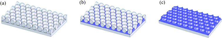 | ||
| Scheme 1 (a) PS beads spin-coated onto an ITO substrate. (b) Electrodeposition of PEDOT. The PEDOT molecules condensed on the ITO substrate between the intervals of the PS beads. The depositing charge density was controlled to ensure that the thickness of the PEDOT film was approximately half the diameter of each bead. (c) Removal of PS beads through soaking in toluene for 12 h. | ||
The PEDOT layer was electrodeposited onto the ITO substrate featuring ordered PS beads by applying a potential of 1.0 V (vs. Ag/AgCl) with a Pt counter electrode until a charge density of 10 mC cm2 was reached. The bath solution was deionized water containing 0.1 M LiClO4 (Aldrich, 95+%), 0.01 M 3,4-ethylenedioxythiophene (EDOT, Aldrich), and 1 wt% sodium dodecyl sulfate (SDS) as surfactant. After the PEDOT film had been deposited, the substrate was immersed into pure toluene for 12 h to remove the PS beads. The remaining PEDOT film possessed a bowl-like structure.7
Different quantities of PANI with various charge densities were deposited on the structured PEDOT films from a bath solution of deionized water containing 1.0 M C6H5NH2 (Lancaster, 99+%) and 2.0 M HCl. The deposition was performed through a pulse procedure consisting of alternating 1 s “current on” and 1 s “current off” stages, with the current density set at 0.1 mA cm−2 during the “current on” stage. The pulse deposition of PANI was stopped when the system reached a set charge density. After depositing PANI, the substrate was cleaned with 0.1 M aqueous HCl and then rinsed with MeCN.7 The uniformity of electrodeposition process controls the application area, a platinum sheet counter electrode with similar size compared with the working electrode can ensure uniformity of polymer film.
2.2 Characterization
Surface morphologies of the nanostructures were measured using a scanning electron microscope (FEI Nova200) and an atomic force microscope (Veeco diInnova; tip condition: tapping mode, 320 kHz resonance frequency and 42 N m−1 force constant). CV and EIS studies were performed at 25 °C using a three-electrode cell with 0.5 M LiClO4 in MeCN as the electrolyte, a fabricated electrochromic film as the working electrode, a Pt sheet as the counter electrode, and nonaqueous Ag/Ag+ (containing 0.01 M AgNO3 and 0.1 M TBAClO4 in MeCN) as the reference electrode. Electrochemical studies were carried using a potentiostat (AUTOLAB PGSTAT 302N). Spectroelectrochemical data were recorded using a Shimadzu UV-1601PC spectrophotometer.3. Results and discussion
We prepared the PS template by spin-coating PS beads onto the surface of indium tin oxide (ITO) substrates. The scanning electron microscopy (SEM) images in Fig. 1 (a) and (c) reveal that the most of the ITO surface was covered by a monolayer of PS beads and that the PS beads were paved periodically. Next, we used electrochemical deposition to grow the PEDOT layer from the conductive ITO surface, until all of the interstices of the first layer of PS beads had been filled. After electrochemical deposition, we removed the PS beads through washing with toluene to leave a pure PEDOT film featuring many small holes, which covered the entire ITO surface with high periodicity (Fig. 1 (b) and (d)).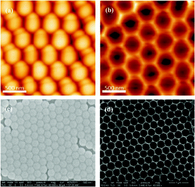 | ||
| Fig. 1 (a, b) AFM and (c, d) SEM images of (a, c) PS beads and (b, d) structured PEDOT (without PS beads) on the ITO surface. | ||
After manufacturing the structured PEDOT films, we used pulsed electrochemical deposition to deposit different amounts of PANI. Fig. 2 (a) displays the electrochemical properties of pristine PEDOT and PANI, recorded using cyclic voltammetry (CV); Fig. 2 (b) displays the CV behavior of PEDOT–PANI composite films prepared without the nanostructure. The reduction current decreased upon increasing the amount of PANI. The reduction current was absent after we had deposited PANI at 5 mC cm2; at this level, PANI had not yet fully covered the surface of the PEDOT layer (i.e., the uncovered PEDOT could still contact the electrolyte). When the thickness of the PANI top layer increased, the reduction current of PEDOT that started at −0.75 V decreased dramatically, such that we could see only the oxidation and reduction peaks of PANI. This situation arose because PEDOT is not conductive in the reduced state; as a result, it formed an impedance layer under the PANI film and we could not observe even the reduction current of PANI that started at −0.8 V. In contrast, the reduction currents of PEDOT–PANI composite films with the nanostructure were evident for any amount of PANI (Fig. 2 (c)). This finding implies that the structure assisted both the PEDOT and PANI films to come into contact with the electrolyte, allowing their electrochemical properties to be observed through CV. When the pulse setting for depositing PANI was greater than 25 mC cm2, the reduction current was lower than that obtained at 20 mC cm2, suggesting that the surface area of PEDOT exposed to the electrolyte began to decrease at this level. Higher pulse conditions further suppressed the electrochemical behavior of PEDOT as a result of greater PANI coverage.
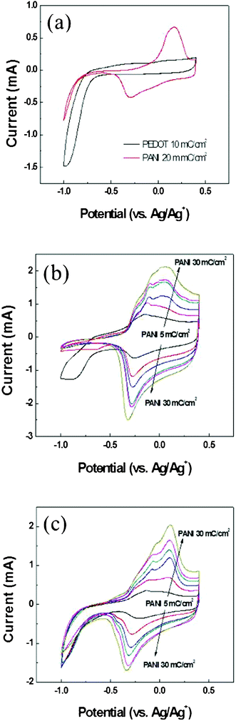 | ||
| Fig. 2 CV characteristics of (a) planar PEDOT and PANI films, (b) bilayer PEDOT–PANI composite films prepared without the nanostructure, and (c) bilayer PEDOT–PANI composite films prepared with the nanostructure. In (b) and (c), the deposition charge density of PEDOT was held constant (10 mC cm2), while that of PANI was varied (5, 10, 15, 20, 25, 30 mC cm2). | ||
The presence of nanostructures on PEDOT and PANI affected not only on their electrochemical properties but also their optical properties. Fig. 3 (a) and (b) present the UV-Vis absorption spectra of pristine PEDOT and PANI recorded under applied potentials between −0.1 and +0.4 V (vs. Ag/Ag+) in 0.1 M LiClO4 in MeCN. The characteristic peak of PEDOT in its reduction state appeared at 600 nm; the absorption intensity of PANI increased upon increasing the positive applied potentials. In contrast, when we stacked these two materials in the absence of the nanostructure, the absorption intensities barely changed upon varying applied potentials (Fig. 3 (c)). Fig. 3 (d) presents the absorption spectra of the composite films constructed with 10 mC cm2 PEDOT and 10 mC cm2 PANI; the composite film prepared with the nanostructure clearly displays the behavior of both the PANI and PEDOT films under the various applied potentials.
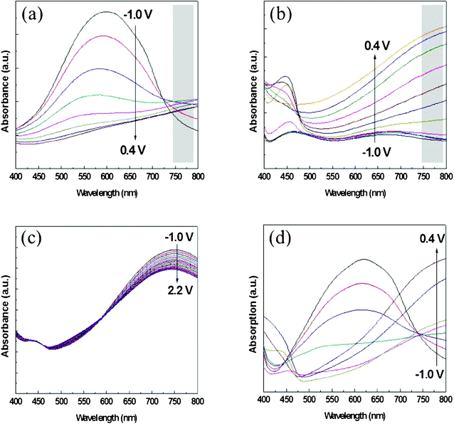 | ||
| Fig. 3 Absorption spectra of (a) pristine PEDOT, (b) pristine PANI, (c) PEDOT–PANI composite films prepared without the nanostructures, and (d) PEDOT–PANI composite films prepared with the nanostructures. | ||
To investigate the PANI growth mechanism on the nanostructured PEDOT film, we prepared composite films with a constant amount (10 mC cm2) of the PEDOT bottom layer and various amounts (5, 10, 15, 20, 25, 30 mC cm2) of the PANI top layer and observed their surface morphologies. Fig. 4 presents SEM images of these PEDOT–PANI composite films. Upon increasing the deposited charge density of PANI, the rims of the structure became thicker, suggesting that the PANI monomers condensed on the rim of each circle, presumably because the edge of the nanostructure had a higher charge density than that in the bowl-like bottom under the applied pulsed potential (i.e., the so-called charge concentration effect).21,22 Thus, the monomers tended to condense on the rim of the nanostructure, with only a slight amount of PANI appearing at the bottom surface of the nanostructure. Upon increasing the depositing charge density, the rims of the nanostructure became plumper and the charge density decreased; as a result, the PANI monomers condensed to a greater degree on both the rims and the bottom surface, causing small grains to form on the bottom of the nanostructure (e.g., see Fig. 4 (f)). From these SEM images, we infer that the PEDOT bottom layer was exposed to the electrolyte only when the PANI top layer was distributed on the rim of the nanostructure. When we increased the depositing charge density, however, the number of PANI monomers that condensed on the bottom gradually increased. In the cases when we deposited PANI as the top layer at 25 and 30 mC cm2, the small grains on the bottom surface covered the PEDOT film and weakened its electrochemical properties, as evidenced by the decrease in the reduction current in Fig. 2 (c).
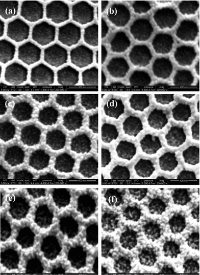 | ||
| Fig. 4 SEM images of structured PEDOT–PANI composite films incorporating PEDOT at 10 mC cm2 and PANI at (a) 5, (b) 10, (c) 15, (d) 20, (e) 25, and (f) 30 mC cm2. | ||
With the different deposited charge densities of PANI, we obtained different absorption spectra. Fig. 5 displays the absorption behavior of PEDOT–PANI composite films featuring a constant amount of PEDOT (10 mC cm2) and different amounts of PANI. Upon increasing the amount of PANI, its characteristics became more dominant. In the range of applied potentials between −1.0 and +0.4 V (vs. Ag/Ag+), the absorption intensities of PEDOT and PANI at 750–800 nm were both higher at 0.4 V and lower at −1.0 V, as revealed earlier in the shadowed boxes of Fig. 3 (a) and (b). This approach allowed us to quantify how the nanostructures enhanced the optical properties of both PEDOT and PANI such that they approached the theoretical values. We prepared pristine PEDOT (10 mC cm2) and PANI (5–30 mC cm2) films without the nanostructure and calculated their coloration efficiencies between −0.1 and 0.4 V (vs. Ag/Ag+) in 0.1 M LiClO4 in MeCN using the following equations:
 | (1) |
 | (2) |
 | (3) |
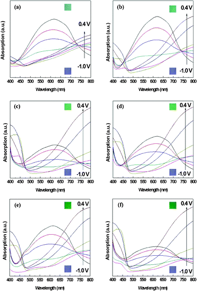 | ||
| Fig. 5 Absorption spectra of the nanostructured PEDOT–PANI composite films featuring PEDOT at 10 mC cm2 and PANI at (a) 5, (b) 10, (c) 15, (d) 20, (e) 25, and (f) 30 mC cm2 under applied potentials ranging from −1 to +0.4 V (vs. Ag/Ag+) in 0.1 M LiClO4 in MeCN. The inset small boxes are the photographs of the composite film (with nanostructure) with different charge densities of PANI under −1.0 V (blue) and 0.4 V (different shades of green) vs. Ag/Ag+. | ||
where CE is the coloration efficiency of a film, Tb is the transmittance of a certain material in its bleached state, Td is the transmittance of a certain material in its darkened state, Q is the charge input to transfer the film from its bleached to darkened states, and A is the working area of the film.
Fig. 6 (a) presents a plot of the measured coloration efficiencies recorded between −1.0 and +0.4 V (vs. Ag/Ag+) in 0.1 M LiClO4 in MeCN. We calculated the theoretical coloration efficiency by substituting the transmittance data from pristine PEDOT and PANI with six different depositing charge densities into eqn (3). We then measured the coloration efficiencies of composite films featuring PEDOT (10 mC cm2) bottom layers and PANI (5, 10, 15, 20, 25, 30 mC cm2) top layers prepared both with and without the nanostructures. The coloration efficiencies of the nanostructured composite films were much closer to the theoretical value than those without the nanostructure, presumably because the resistance of a PEDOT–PANI composite film without the nanostructures was much higher than that of the corresponding system with the nanostructures. Fig. 6 (b) presents EIS plots of PEDOT–PANI composite films prepared with and without nanostructures; both samples featured PEDOT (10 mC cm2) on the bottom and PANI (10 mC cm2) on the top, and the EIS experiment was done under open circuit in order to observe only resistances of structured films and non-structured films and to neglect the interference contributed by the oxidation or reduction of the polymer.
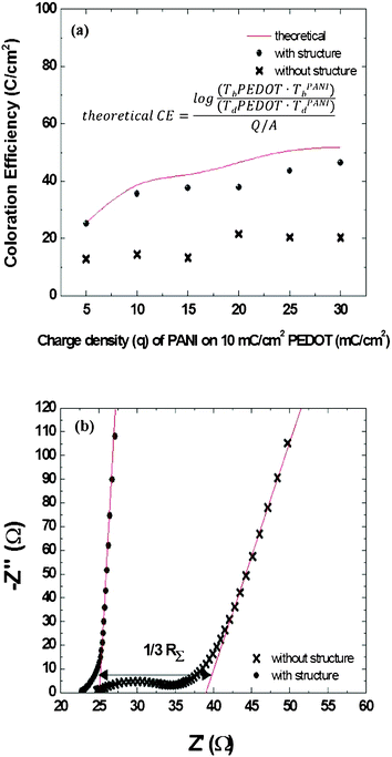 | ||
| Fig. 6 (a) Coloration efficiencies of PEDOT–PANI composite films prepared with and without nanostructures. The amount of PEDOT was fixed at 10 mC cm2; that of PANI was varied from 5 to 30 mC cm2. The theoretical coloration efficiency was obtained by applying transmittance data into the inset equation. (b) Electrochemical impedance spectral analysis of PEDOT–PANI composite films (PEDOT: 10 mC cm2; PANI: 10 mC cm2) prepared with and without nanostructures. | ||
The ionic resistance of the PEDOT–PANI composite film prepared without the nanostructure was much higher than that with the nanostructures. Furthermore, the EIS plot of the composite film prepared without the nanostructures contained an arc response, which was contributed by the charge transfer on the interface of polymer and electrolyte, implying that the PEDOT bottom layer possessed high resistance in the composite film prepared without the nanostructures because of its poor contact with the electrolyte.23 We calculated the ionic transport from the high-frequency real-axis intercept (Rhigh) and the low-frequency limiting real impedance (Rlow) as follows:24
| Rlow − Rhigh = 1/3R | (4) |
The calculated ionic resistances of the composite films prepared with and without the nanostructures were 7.5 and 42.4 Ω, respectively. The nanostructured composite films offered space for the transfer of cations and anions during the redox reaction, leading to lower ionic resistance, which could enhance the reversibility of ionic transfer and, thereby, ensure better long-term stability.25 In addition to recording optical spectra, we also performed colorimetry analyses, which reveal the critical characteristics of dual-colored films.26 We fixed the amount of PEDOT at 10 mC cm2 and used various deposition charge densities of PANI (5, 10, 15, 20, 25, 30 mC cm2) to obtain composite films with different shades of green. When we applied a potential of −1.0 V (vs. Ag/Ag+) to the films, they all turned the same shade of blue because each composite film contained the same amount of PEDOT. When we changed the applied potential to +0.4 V (vs. Ag/Ag+), the films displayed different shades of green. Fig. 7 presents these values in the form of CIE coordinates.
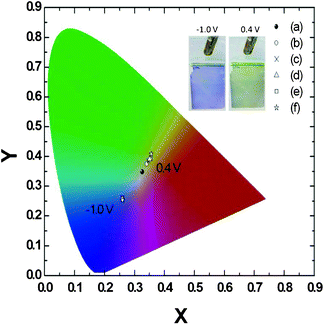 | ||
| Fig. 7 CIE characteristics of structured PEDOT–PANI composite films incorporating a constant amount of PEDOT (10 mC cm2) and PANI contents of (a) 5, (b) 10, (c) 15, (d) 20, (e) 25, and (f) 30 mC cm2. The samples exhibited almost the same color of blue under an applied potential of −1.0 V (vs. Ag/Ag+), but exhibited different shades of green depending on the amount of deposited PANI under an applied potential of 0.4 V (vs. Ag/Ag+). The inset picture shows the composite film with the nanostructure under −1.0 V and 0.4 V (vs. Ag/Ag+). | ||
Fig. 8 (a) displays the switching of the composite films, prepared with and without the nanostructures, between +0.4 and −1.0 V at an interval of 10 s in 0.1 M LiClO4 in MeCN, under 600 nm incident light. Each of these composite films had been constructed with a PEDOT (10 mC cm2) bottom layer and a PANI (10 mC cm2) top layer (Table 1 shows the transmittances data of these samples averaged by 5 different samples of same conditions in order to prove its reproducibility). For the composite film featuring the nanostructure, a large difference in transmittance still appeared after 50 cycles of operation; in contrast, for the composite film lacking the nanostructure, the difference in transmittance (Δ% T) decayed dramatically after each cycle, reaching only 3% transmittance difference after the third cycle. Moreover, the composite films prepared with and without the nanostructures provided values of Δ% T of 27 and 13%, respectively, after the first cycle. The great difference in the performances of these composite films suggests that the nanostructure contributed to improving the electrolyte diffusion. The composite film featuring the nanostructure came into better contact with the electrolyte than that without the nanostructure, resulting in a higher doping level, superior ionic transfer, a higher value of Δ% T, and improved stability.23Fig. 8 (b) reveals that the switching time (defined as the time between Tmin and 90% Tmax) of the composite film prepared with the nanostructure was 0.9 s, much shorter than that of the film prepared without the nanostructure (1.9 s), again implying that the electrolyte penetrated efficiently into the composite film through the fabricated nanostructure. The research of lifetime and long term stability which relate to more environmental factors (such as the species of ions, solvents, charge densities of each polymer layer, and operating potential window…etc.) is under progress.
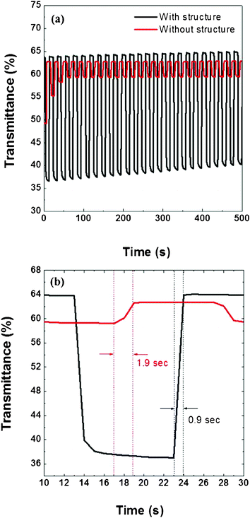 | ||
| Fig. 8 (a) Switching stability of PEDOT–PANI composite film (PEDOT: 10 mC cm2; PANI: 10 mC cm2) prepared with and without nanostructures. (b) Enlarged view of one switching cycle from (a); dashed lines reveal the change in the composite films between their darkened and bleached states; with structure (black), without structure (red). The time range between the dashed lines reveals the transmittance differences (ΔT) from the minimum transmittance (Tmin) to 90% of the maximum transmittance (T90%). For the composite film prepared without the nanostructure, it took 1.9 s to switch from Tmin to T90%; for the composite film prepared with the nanostructure, only 0.9 s elapsed in the change from Tmin to T90%. | ||
| Sample | Tb (%) | Td (%) | ΔT (%) |
|---|---|---|---|
| With nanostructure | 64.3 ±0.5 | 38.6 ±2.0 | 25.7 ± 3.0 |
| Without nanostructure | 62.7 ±0.1 | 59.4 ±0.1 | 3.3 ± 0.2 |
4. Conclusions
We have developed electrochromic films exhibiting a dual colored state through the deposition of PANI on the rims of a nanometer-scale honeycomb PEDOT layer. The composite film appeared green in its oxidation state and blue in its reduction state. The coloration efficiencies of composite films prepared with the nanostructures were quite close to the theoretical values obtained for pristine PEDOT and PANI single layers with corresponding charge densities. The composite film prepared with the nanostructure retained its high transmittance change upon repeated switching, whereas the composite film lacking the nanostructure did not. The presence of the nanostructure allowed both materials to come into good contact with the electrolyte, thereby decreasing the resistance within the film and resulting in each material revealing its own properties. Our reported strategy for fabricating periodic polymer nanostructures should be applicable to the preparation of multi-color electrochromic films through electrochemical pulse deposition of other polymers onto the rims of nanostructures.Acknowledgements
We thank the National Science Council (NSC), Taiwan (100-2120-M-009-004), and the Academia Sinica research program on nanoscience and nanotechnology for financial support.References
- L. B. Groenendaal, F. Jonas, D. Freitag, H. Pielartzik and J. R. Reynolds, Adv. Mater., 2000, 12, 481 CrossRef CAS.
- L. B. Groenendaal, G. Zotti, P. H. Aubert, S. M. Waybright and J. R. Reynolds, Adv. Mater., 2003, 15, 855 CrossRef CAS.
- E. S. Lee and D. L. DiBartolomeo, Sol. Energy Mater. Sol. Cells, 2002, 71, 465 CrossRef CAS.
- T. Kubo, J. Tanimoto, M. Minami, T. Toya, Y. Nishikitani and H. Watanabe, Solid State Ionics, 2003, 165, 97 CrossRef CAS.
- P. M. S. Monk, R. J. Mortimer, D. R. Rosseinsky, Electrochromism and electrochromic devices, Cambridge University Press, Cambridge, UK, 2007 Search PubMed.
- A. L. Dyer and J. R. Reynolds, in Handbook of conducting polymers, ed. T. A. Skotheim and J. R. Reynolds, CRC Press, Boca Raton, FL, 3rd edn, 2007, vol. 1, ch. 20 Search PubMed.
- T. H. Lin and K. C. Ho, Sol. Energy Mater. Sol. Cells, 2006, 90, 506 CrossRef CAS.
- S. Xiong, J. Ma and X. Lu, Sol. Energy Mater. Sol. Cells, 2009, 93, 2113 CrossRef CAS.
- S. F. Hong, S. C. Hwang and L. C. Chen, Electrochim. Acta, 2008, 53, 6215 CrossRef CAS.
- N. Leventis and Y. C. Chung, J. Mater. Chem., 1993, 3, 833 RSC.
- V. Jain, M. Khiterer, R. Montazami, H. M. Yochum, K. J. Shea and J. R. Heflin, ACS Appl. Mater. Interfaces, 2009, 1, 83 CAS.
- T. Brezesinski, D. F. Rohlfing, S. Sallard, M. Antonietti and B. M. Smarsly, Small, 2006, 2, 1203 CrossRef CAS.
- S. L. Kuai, G. Bader and P. V. Ashrit, Appl. Phys. Lett., 2005, 86, 221110 CrossRef.
- X. H. Xia, J. P. Tu, J. Zhang, J. Y. Xiang, X. L. Wang and X. B. Zhao, ACS Appl. Mater. Interfaces, 2009, 2, 186 Search PubMed.
- P. N. Bartlett, P. R. Birkin, M. A. Ghanem and C. S. Toh, J. Mater. Chem., 2001, 11, 849 RSC.
- J. Yang and D. C. Martin, Sens. Actuators, B, 2004, 101, 133 CrossRef.
- P. Jia, A. A. Argun, J. Xu, S. Xiong, J. Ma, P. T. Hammond and X. Lu, Chem. Mater., 2009, 21, 4434 CrossRef CAS.
- E. L. Ratcliff, J. L. Jenkins, K. Nebesny and N. R. Armstrong, Chem. Mater., 2008, 20, 5796 CrossRef CAS.
- C. W. Kuo, K. H. Wei, C. H. Lin, J. Y. Shiu and P. Chen, Electrophoresis, 2008, 29, 2931 CrossRef CAS.
- C. W. Kuo, J. Y. Shiu, F. C. Chien, S. M. Tsai, D. Y. Chueh and P. Chen, Electrophoresis, 2010, 31, 3152 CrossRef CAS.
- Y. M. Lim and S. H. Kim, Int. J. Mach. Tools Manuf., 2001, 41, 2287 CrossRef.
- C. A. Huang, J. H. Chang, S. Y. Yang and C. C. Yang, Corros. Sci., 2006, 48, 4294 CrossRef CAS.
- R. Hass, J. G. Cannadas and G. G. Belmonte, J. Electroanal. Chem., 2005, 577, 99 CrossRef CAS.
- V. Noel, H. Randriamahazaka and C. Chevrot, J. Electroanal. Chem., 2003, 558, 41 CrossRef CAS.
- J. H. Huang, C. Y. Hsu, C. W. Hu, C. W. Chu and K. C. Ho, ACS Appl. Mater. Interfaces, 2010, 2, 351 CAS.
- J. H. Huang, C. Y. Yang, C. Y. Hsu, C. L. Chen, L. Y. Lin, R. R. Wang, K. C. Ho and C. W. Chu, ACS Appl. Mater. Interfaces, 2009, 1, 2821 CAS.
| This journal is © The Royal Society of Chemistry 2012 |