DOI:
10.1039/C1RA00161B
(Paper)
RSC Adv., 2012,
2, 941-948
Correlation between microstructure, electrical and optical properties of nanocrystalline NiFe1.925Dy0.075O4 thin films
Received
10th May 2011
, Accepted 6th October 2011
First published on 28th November 2011
Abstract
Dysprosium-doped nickel-ferrite (NiFe1.925Dy0.075O4) thin films were fabricated using sputter-deposition using a stoichiometric bulk target prepared by the solid state chemical reaction. The structural, electrical and optical properties of NiFe1.925Dy0.075O4 thin films were studied in detail. The grain-size (L) and lattice-expansion effects are significant on the electrical and optical properties of NiFe1.925Dy0.075O4 films. Air annealing (Ta) at 450–1000 °C results in the formation of nanocrystalline NiFe1.925Dy0.075O4 films, which crystallize in the inverse spinel structure, with L = 5–40 nm. The lattice constant of NiFe1.925Dy0.075O4 increases compared NiFe2O4 due to Dy-doping. Electrical conductivity of NiFe1.925Dy0.075O4 films (at 300 K) decreases from 1.07 Ω−1 m−1 to 3.9 × 10⁻³ Ω−1 m−1 with increasing Ta (450 to 1000 °C). Conductivity was found to decrease exponentially with decreasing the temperature from 300 K to 120 K indicating the characteristic semiconducting nature of all the films. Band gap increases from 3.17 to 4.08 eV for NiFe1.925Dy0.075O4 films with increasing Ta from 450 to 1000 °C. A correlation between grain-size, electrical conductivity and optical band gap in nanocrystalline NiFe1.925Dy0.075O4 films is established.
1. Introduction
Nickel (Ni) and cobalt (Co) based ferrites have been the subject of intense research in recent years due to their wide range of scientific and technological applications.1–15 Ferrite materials find high frequency applications due to their high permeability and permittivity.1–8 These materials are being used in transformer cores, antennas, radio frequency coil and radar absorbing materials (RAM).1–6 Due to their low eddy current losses, nanostructured NiFe2O4 thin films are important candidates for magnetic components such as resonators, phase shifters, tunable signal filters and, most recently, for spintronics applications.1–11 These properties also make them unique in microwave devices that require strong electromagnetic signal coupling.1–11 Along with diverse applications, ferrites have properties which are of fundamental interest. For instance, a small change in stoichiometry and size makes the magnetic and electronic properties of ferrite tunable.1–11 Furthermore, the effects of cationic interchange and oxygen vacancies lead to unusual magnetic properties when these materials are fabricated as thin films and nano-particles. However, these properties and the performance of ferrite thin films are very sensitive to growth conditions, method of preparation and the associated chemistry.1–11
In Ni ferrite, the tetrahedral (A) sites are occupied by the Fe3+ ions and the octahedral sites (B) are occupied by the Ni2+ and Fe3+, in equal proportions.1,2 Partial substitution of Fe3+ by a rare-earth ion can significantly modify the electrical and dielectric properties of Ni ferrites.7–16 It has been reported that, inclusion of Zn, Cu, Co and Cd in ferrites,17,18 (Ni ferrite, Ni–Zn ferrite, Ni–Cu ferrite and Li–Ni–Cd ferrite) leads to an increase in the dielectric constant and dielectric loss due to the formation of excess Fe2+, which leads to an increase in the hopping of electrons between Fe2+ and Fe3+. Partial substitution of Fe3+ by rare earth ions in the spinel structure has been reported to lead to structural distortion7–14 that induces strain and significantly modifies the electrical and dielectric properties.7–15
The present work was performed on the effect of Dy ion substitution at the Fe site on the structural characteristics, electrical and optical properties of Ni ferrite (NiFe1.925Dy0.075O4) films. Impetus is to derive the structure–property relationship, which in turn depends on growth, composition and structure at reduced dimensions, in NiFe1.925Dy0.075O4 films for their utilization in device applications. A detailed account of the crystal structure, surface morphology, electrical and optical properties of amorphous and nanocrystalline NiFe1.925Dy0.075O4 films is presented and discussed in this paper.
2. Experimental details
2.1 Target (bulk) material synthesis
NiFe1.925Dy0.075O4 materials were synthesized by the conventional solid state chemical reaction method. The starting materials were 99.99% pure NiO, Fe2O3 and Dy2O3 powders, which were weighed in their stoichiometric ratio. Powders were then mixed together and ground in a mortar and pestle for one hour and heat treated in air at 1200 °C for 12 h. After the heat treatment, the powders were allowed to settle down to room temperature. The powders thus obtained were made into a target of 2′′ diameter and then sintered at 1250 °C in air for 12 h. The sintered pellet was used as a target for the thin film preparation by sputter-deposition. In order to reduce the formation of secondary phase (DyFeO3) and to get improved electrical and dielectric properties13, 3.5% Dy3+ was substituted for Fe3+ (NiFe1.925Dy0.075O4).
2.2 Thin film fabrication
NiFe1.925Dy0.075O4 films were deposited onto silicon (Si) (100) and optical grade quartz substrates by radio-frequency (RF) (13.56 MHz) magnetron-sputtering. The films grown on Si were used for XRD, AFM and electrical measurements. The films grown on quartz were used for the optical measurements. The deposition conditions were listed in Table 1. All the substrates were thoroughly cleaned, as per the procedure reported elsewhere, and dried with nitrogen before introducing them into the vacuum chamber, which was initially evacuated to a base pressure of ∼10−6 Torr. The ferrite target was placed on a 2 inch sputter gun, which is placed at a distance of 8 cm from the substrate. A sputtering power of 40 W was initially applied to the target while introducing high purity argon (Ar) into the chamber to ignite the plasma. Once the plasma was ignited the power was increased to 100 W and oxygen (O2) was released into the chamber for reactive deposition. Deposition was made at room temperature (RT) to obtain a ∼50 nm thick film. NiFe1.925Dy0.075O4 films prepared at RT were air-annealed (one hour) in the temperatures (Ta) range 450–1000 °C.
Table 1 Sputter-deposition conditions employed for NiFe1.925Dy0.075O4 films
| Deposition parameter |
Set value |
| Base pressure |
∼10−6 Torr. |
|
Sputtering pressure |
∼10−3 Torr. |
| Target |
NiFe1.925Dy0.075O4 films |
| |
(2′′ × 0.125′′) |
| Substrates |
Si(100) and Quartz |
| Substrate temperature (Ts) |
Room temperature |
| Target–substrate distance |
8 cm |
| RF power |
100 W |
| Film thickness |
∼50 nm |
|
Annealing temperature (Ta) |
450–1000 °C |
| Ar:O2 ratio |
90![[thin space (1/6-em)]](https://www.rsc.org/images/entities/char_2009.gif) :10 :10 |
2.3 Characterization
NiFe1.925Dy0.075O4 films were studied to evaluate their structural, electrical and optical properties. Crystal structure and density measurements were made using grazing incidence X-ray diffraction (GIXRD) and X-ray reflectivity (XRR) measurements, respectively. The GIXRD and XRR measurements on NiFe1.925Dy0.075O4 films were performed using a Bruker D8 Advance X-ray diffractometer. XRD patterns were recorded using Cu Kα radiation (λ = 1.54056 Å) at RT. The coherently diffracting domain size (dhkl) was calculated from the integral width of the diffraction lines using the well known Scherrer equation16 after background subtraction and correction for instrumental broadening. The Scherrer equation is:
where
dhkl is the size,
λ is the wavelength of the X-rays used,
β is the width of a peak at half of its intensity, and
θ is the angle of the peak. Surface imaging was performed using an
Atomic Force Microscope (
AFM) (Nanoscope IV-Dimension 3100
SPM system). Interface morphology is primarily obtained from
scanning electron microscopy (
SEM). Imaging was performed using a high-performance and ultra high resolution
scanning electron microscope (Hitachi S-4800). The secondary electron imaging was performed on NiFe
1.925Dy
0.075O
4 films grown on Si wafers. DC electrical resistivity measurements were carried out under the vacuum of 10
−2 Torr by two-probe method in the temperature range 60–300 K employing a closed cycle refrigerator (CCR). All the measurements were carried out during the heating cycle and equilibrium was reached by allowing one minute at each temperature measurement. Resistance was measured by employing a Keithley electrometer (Keithley 6517A Electrometer/High resistance meter). The temperature was measured using a silicon diode sensor and employing a Lakeshore temperature controller (Model No. 330). The film was kept on the cold head of the CCR. The point contacts were made by soldering the indium metal at the corners of the films.
3. Results and discussion
3.1 Crystal structure and surface/interface morphology
The XRD patterns of NiFe1.925Dy0.075O4 films are shown in Fig. 1. The XRD curves of NiFe1.925Dy0.075O4 films grown at RT did not show any peaks indicating their characteristic amorphous nature (Fig. 1). The XRD peaks began to appear for samples annealed at Ta = 450–1000 °C indicating the crystallization of NiFe1.925Dy0.075O4 films upon annealing. The peaks can be unambiguously assigned to face centered cubic (FCC) inverse spinel phase.12–15 Comparison of the XRD data with that of pure NiFe2O4 films and bulk (JCPDS Card No. 86-2267) indicates the expected peaks of spinel NiFe2O4 for NiFe1.925Dy0.075O4 films (as labeled in Fig. 1). The evolution of XRD peaks indicate that the average grain-size (L) increases with increasing annealing temperature. The grain size increases from 5 to 40 nm with increasing Ta from 450 to 1000 °C. The lattice constant (a) derived from XRD for nanocrystalline NiFe1.925Dy0.075O4 films showed an interesting behavior as a Ta. For NiFe1.925Dy0.075O4 films, ‘a’ increases linearly from 8.353 (± 0.001) to 8.362(± 0.001) Å with increasing Ta from 450 to 1000 °C. The lattice constant obtained for NiFe1.925Dy0.075O4 films annealed at 450 °C, where the onset of crystallization and inverse spinel phase formation occurs, can be compared to that of pure NiFe2O4 to see the effect of Dy-substitution. The lattice constant of NiFe1.925Dy0.075O4 films at Ta = 450 °C is 8.353 Å while that of NiFe2O4 is 8.340 Å.12,13,17 This observation indicates the lattice expansion upon Dy-doping. Increased lattice constant upon Fe3+ substitution by Dy3+ is due to the larger ionic size of Dy3+ (1.05 Å) compared to that of Fe3+ (0.63 Å). Such behavior is also noticed in Sm and Ho substituted Ni-ferrites.12 Further increase in the lattice constant with Ta may be due to the lattice-strain developed in the nanocrystalline NiFe1.925Dy0.075O4 films at higher Ta. The AFM images of NiFe1.925Dy0.075O4 films are shown in Fig. 2. The effect of Ta on the surface morphology of NiFe1.925Dy0.075O4 films is remarkable. For annealed samples, presence of the small, dense particles can be noticed in AFM images. The fine microstructure and uniform distribution characteristics of the particles are evident in the micrographs (Fig. 2). The average particle size is 5–32 (± 0.3) nm, which agrees with the calculated L values from the XRD data. As-grown films exhibit featureless images (not shown) indicating the characteristic amorphous phase.
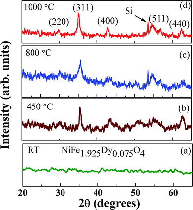 |
| | Fig. 1
XRD patterns of NiFe1.925Dy0.075O4 films. It is evident from the curves that the films grown at RT are amorphous whereas films anealed at Ta ≥ 450 °C are nanocrystalline, crystallize in inverse spinel phase | |
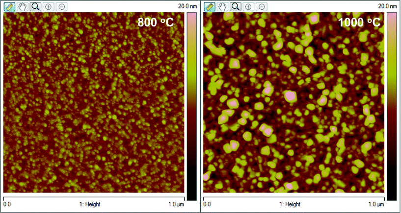 |
| | Fig. 2 High resolution AFM images of NiFe1.925Dy0.075O4 films annealed at different temperatures. The effect of Ta on the surface morphology of NiFe1.925Dy0.075O4 films is evident. | |
The XRR plots of NiFe1.925Dy0.075O4 films are shown in Fig. 3a. The following observations can be made from the XRR spectra. A positive shift (higher angle) of the critical edge with increasing annealing temperature or grain size is the first. The positive shift of the critical edge indicates an increase in the film density with increasing annealing temperature. Simulation of the XRR curves allows obtaining thickness and density of the NiFe1.925Dy0.075O4 films. Simulation of XRR data indicates that the as-grown, amorphous NiFe1.925Dy0.075O4 films at RT are ∼50 nm while thickness slightly decreases for those films annealed at 800 and 1000 °C. The density of NiFe1.925Dy0.075O4 films as a function of Ta is shown in Fig. 3b. Density is seen to increase from 3.181 to 3.814 g cm−3 with increasing Ta due to an increase in packing. Roughness of the film is found to increase with increasing Ta. A comparison of the physical parameters obtained from XRR and AFM measurements are presented in Table 2.
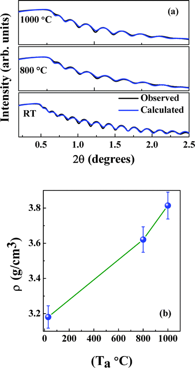 |
| | Fig. 3 (a) The XRR plots of NiFe1.925Dy0.075O4 films. The positive shift of the critical edge indicates an increase in the film density with increasing annealing temperature. (b) Variation of density of NiFe1.925Dy0.075O4 films with increasing annealing temperature. Density of NiFe1.925Dy0.075O4 films are found to increase with increasing Ta. | |
Table 2 Thickness and roughness values of NiFe1.925Dy0.075O4 films calculated and observed from XRR and AFM measurements
|
Ta (°C) |
Thickness (nm) |
Roughness |
|
AFM
|
XRR (nm) |
| RT |
49 |
— |
1.299 |
| 800 °C |
40 |
1.26 |
1.34 |
| 1000 °C |
40 |
3.01 |
1.86 |
The SEM cross-sectional images of the representative NiFe1.925Dy0.075O4 films are shown in Fig. 4. Images shown are obtained for NiFe1.925Dy0.075O4 films grown at room temperature and NiFe1.925Dy0.075O4 films air-annealed at 1000 °C. The Si-substrate and NiFe1.925Dy0.075O4 film regions are as indicated in the micrographs. While slightly reduced film thickness is obviously seen for NiFe1.925Dy0.075O4 films annealed at the highest temperature of 1000 °C, no evidence of significant reaction with the Si-substrate at the interface is seen in either for annealed or as-grown samples. This observation indicates that the NiFe1.925Dy0.075O4 films are stable with the Si substrate within the given set of conditions employed in this work.
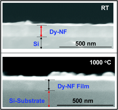 |
| | Fig. 4 The SEM cross-sectional images of NiFe1.925Dy0.075O4 films. (a) RT and (b) Ta = 1000 °C. The Si-substrate and the NiFe1.925Dy0.075O4 film regions are as indicated in the micrographs. No significant interfacial reactions or compound formation occurs at the Si–NiFe1.925Dy0.075O4 interface. | |
3.2 DC electrical properties
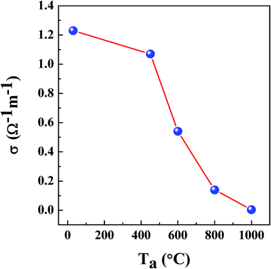
Fig. 5 shows the room temperature dc electrical conductivity variation of NiFe1.925Dy0.075O4 films with annealing temperature. Electrical conductivity of NiFe1.925Dy0.075O4 film is seen to decrease from 1.2 Ω−1 m−1 to 3.9 × 10⁻³ (± 10−6) Ω−1 m−1 with increasing Ta from RT to 1000 °C. Decrease in conductivity with increasing Ta of NiFe1.925Dy0.075O4 can be attributed to the combined effect of Dy incorporation and the strain induced in the films. Substitution of small amounts of Dy3+ ions for Fe3+ ions in B site increases the inter-ionic distances and distorts the lattice due to larger ionic size of Dy3+ compared to that of Fe3+, leading to additional scattering and causing the decrease in electrical conductivity. The conductivity is reported19 to change with grain size reduction due to the increasing grain boundary volume and associated impedance to the flow of charge carriers. If the crystallite size is smaller than the electron mean free path, grain boundary scattering dominates and hence the electrical conductivity decreases. In addition, the contributions to the electrical conductivity from lattice imperfections, such as vacancies and dislocations which were reported to be present in thin films and nanocrystalline materials.18,19
 |
| | Fig. 5 Room temperature DC conductivity values of the NiFe1.925Dy0.075O4 films annealed at different temperature. | |
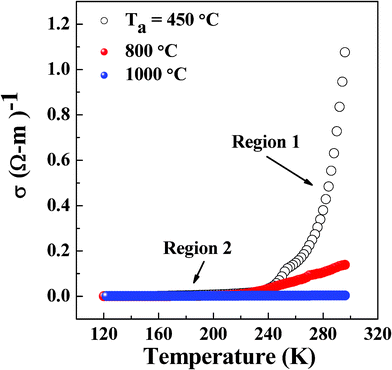
The variation of DC electrical conductivity of NiFe1.925Dy0.075O4 films is shown in Fig. 6. Electrical conductivity decreases exponentially with decreasing the temperature from 300 K to 120 K which indicates the semiconducting nature of the films. Conductivity in semiconductors is due to both hopping of electrons and charge transportvia excited states and it can be expressed as:19,20
 |
| | Fig. 6 Temperature variation of DC conductivity of the NiFe1.925Dy0.075O4 films. Temperature variation of conductivity (from 300 K to 120 K) indicates the semiconducting nature of the films. | |
| |
| (2) |
where E
1 is the activation energy for intrinsic conduction and
E2,
E3,…are the activation energies needed for hopping conduction.
A1,
A2,
A3 are constants and
kB is the Boltzmann constant.
It is evident from the electrical conductivity plot (Fig. 6) that two different slopes exists for both the compounds indicating that the conduction is through an activated process having two difference conduction processes. Activation energy values at different temperature ranges (300–250 K and 250–120 K) were calculated from the lnσ vs 1000/T plot and are given in Table 3. Activation energy values were found to be higher at the 300–250 K region (0.44 eV for the film annealed at 450 °C) and lower at the 250–60 K region (0.1 eV). Decreasing activation energy with decreasing temperature has been explained by small-polaron theory.19,20 The VRH19,20 model of small polarons also predicts continuously decreasing activation energy with decreasing temperature.
Table 3
Activation energy values of NiFe1.925Dy0.075O4 films at different temperature regions
|
Ta (°C) |
Activation Energy (eV) |
| 300–250 K |
250–120 K |
| 450 °C |
0.44 |
0.10 |
| 800 °C |
0.47 |
0.12 |
| 1000 °C |
0.48 |
0.13 |
3.3 AC electrical properties
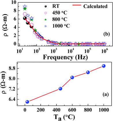
The AC electrical resistivity data of NiFe1.925Dy0.075O4 films are shown in Fig. 7. The variation of resistivity, measured at room temperature, with annealing temperature is shown in Fig. 7(a) while the frequency (20 Hz–1 MHz) dependent resistivity curves are shown in Fig. 7 (b). While the resistivity values are seen to be in the order of Ω m at low frequencies (up to 1 kHz), they are found to decrease to ∼10−2 Ω m at higher frequencies (1 MHz). It is known that in ferrites, the AC conduction is due to the hopping of electrons between ions having different valance (Fe2+/Fe3+, Co2+/Co3+, Ni2+/Ni3+) states. With increasing in frequency, hopping increases and correspondingly the resistivity decreases.
 |
| | Fig. 7 Room temperature AC resistivity values of NiFe1.925Dy0.075O4 films (a). Frequency dependent conductivity of NiFe1.925Dy0.075O4. The dispersion relation is shown with increasing Ta (b). | |
The resistivity data was fit to the following equation 2,10
| |
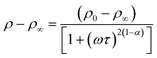
| (3) |
where
ρ∞ is the resistivity value at 1 MHz,
ρ0 is the resistivity value at 20 Hz,
τ is the mean relaxation time and
α is the spreading factor about the mean relaxation time. The calculated mean relaxation time values are found to increase from 2.9 μs to 3.6 μs with increasing T
a from RT to 1000 °C due to the increase in resistivity.
3.4 Optical properties
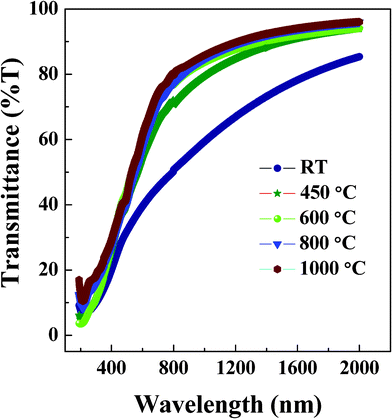
Optical transmittance spectra of NiFe1.925Dy0.075O4 films are shown in Fig. 8. A marked behavior in the spectral transmittance behavior can be seen in NiFe1.925Dy0.075O4 films annealed at 450 °C when compared to that of films grown at RT. Perhaps, a large number of defects resulting from amorphous phase may be affecting the optical quality of the films. In addition, the spectral characteristics of NiFe1.925Dy0.075O4 films are also sensitive to the annealing temperature. Increasing Ta is seen to exhibit higher transparency in the spectral region except where the incident radiation is absorbed across the band gap (Eg). This observation indicates the high-quality and transparent nature of NiFe1.925Dy0.075O4 films with increasing Ta.
 |
| | Fig. 8 Transmittance curves of NiFe1.925Dy0.075O4 films. The curves indicate that the films are highly transparent. | |
A further analysis of the spectral transmittance curves is performed in order to better understand the electronic structure changes as a result of Dy-substitution and variations in film-microstructure upon annealing. It is well known that the optical absorption below Eg follows an exponential behavior.21–24 The absorption, therefore, is exponentially dependent on the energy (hυ) of incident photon in that region. Ni-ferrite is a direct band gap material, which follows the power law of the form:23,24
| | |
(αhυ) = B(hυ − Eg)1/2
| (4) |
where
hυ is the energy of the incident
photon,
α the absorption coefficient,
B the absorption edge width parameter,
Eg the band gap. The optical absorption coefficient,
α, of the films is evaluated using the relation:
21–24
| |
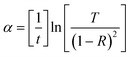
| (5) |
where
T is the transmittance,
R is the reflectance and
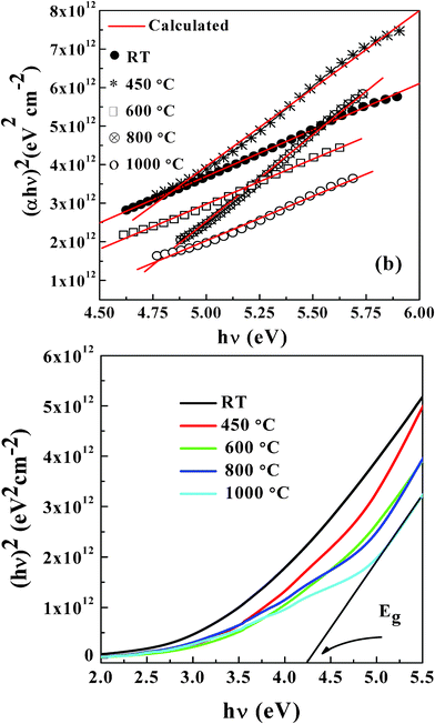
t is the film thickness. The absorption data and the plots obtained for NiFe
1.925Dy
0.075O
4 films are shown in
Fig. 9 (a). The (
αhν)
2versus hν plots exhibit a better fit. Linear regression fit and the extrapolation (
Fig. 8 (b)) of the plot to zero absorption
i.e.,
α (
hν) = 0 provide the
Eg value. Variation of
Eg with
Ta is shown in
Fig. 10. It is evident that
Eg is sensitive to
Ta (
Fig. 8).
Eg = 3.17 eV for amorphous NiFe
1.925Dy
0.075O
4 films grown at RT.
Eg increases to 4.08 eV with increasing
Ta to 1000 °C.
Eg values of NiFe
1.925Dy
0.075O
4 films are larger than those reported for either bulk or thin-film NiFe
2O
4.
23,24
 |
| | Fig. 9 (αhν)2versus E for NiFe1.925Dy0.075O4 films (a). Linear regression fit and the extrapolation of the plot to zero absorption i.e., α (hν) = 0 provide the Eg value (b). | |
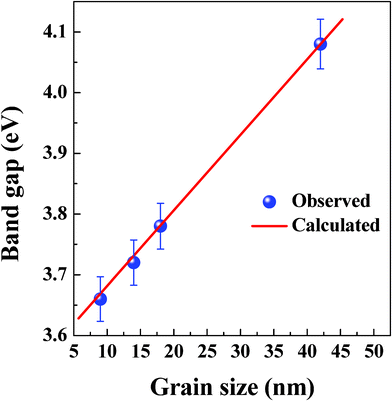 |
| | Fig. 10
L–Eg relationship in NiFe1.925Dy0.075O4 films (a). A direct relationship is evident. | |
A model can be formulated to account for the observed L–Eg and a–Eg relationship and associated chemistry, which in turn establishes the functional structure–property relationship in NiFe1.925Dy0.075O4 films. NiFe2O4 is a semiconductor with Eg = 2.1 eV. The Eg values obtained in the present work are significantly higher compared to this value. The effect of Dy incorporation is clearly the Eg enhancement compared to NiFe2O4. The changes in electronic structure and, hence, Eg within the NiFe1.925Dy0.075O4 films can be explained as follows. It must be emphasized that the Eg value is sensitive to the microstructure; it is influenced by various factors such as surface/interface structure, grain size, crystal quality, lattice parameters, lattice strain, carrier concentrations, defect structure, and chemical composition. XRD measurements clearly indicate that the as grown NiFe1.925Dy0.075O4 films are amorphous. Eg shift to 3.17 eV in NiFe1.925Dy0.075O4 compared to that of pure Ni-ferrite can be attributed to the combined effect of Dy incorporation, amorphous structure and presence of oxygen vacancies. The poor quality of the films due to amorphous nature and oxygen vacancies is also evidenced by the spectral transmittance, which is significantly lower compared to the annealed films. A direct, linear relationship of Ta–Eg, L–Eg and a–Eg is evident from this work (Fig. 10). Structural transformation in NiFe1.925Dy0.075O4 films from amorphous to nanocrystalline at 450 °C coupled with filling up of oxygen vacancies is responsible for the observed increase in Eg. This structural transformation is evidenced by XRD while the improved spectral transmittance accounts for fulfilment of oxygen vacancies due air annealing. A further increase in Ta from 450 to 1000 °C is seen to increase the density, grain size, and lattice parameter. It has been reported23,24 that the band gap (Eg) enhancement in nanostructured materials is due to two factors, quantum confinement and strain. As a result, although the approximation was proposed for spherical nanocrystals, the variation in band gap energy can be written as:
| | | Eg = Eg (Bulk) + ΔEg (I) + ΔEg (II) | (6) |
The ΔEg (I) and ΔEg (II) terms account for the quantum and strain induced effects, respectively. Clearly, the Eg enhancement in the present case with increasing Ta is not due to ΔEg (I) term since the average grain size increases as noted from XRD studies. Since all the films were air-annealed for same amount of time, Eg enhancement with increasing Ta must be associated with the lattice parameter expansion, which leads to the strain in the films. In other words, the second term (ΔEg (II)) of the above equation is at play to induce the observed changes. This accounts for the observed increase in Eg from 3.17 to 4.08 eV for NiFe1.925Dy0.075O4 films with increasing Ta. Such behavior and Eg enhancement is also noticed in transition-metal doped NiFe2O4 films 23–25
4. Conclusions
NiFe1.925Dy0.075O4 films were fabricated using sputter-deposition and their structural and optical properties were investigated. The effect of partial substitution of Dy3+ ions for Fe3+ ions is, in general, lattice expansion associated with lattice strain and enhanced Eg. NiFe1.925Dy0.075O4 films grown at RT were amorphous and oxygen deficient. Air annealing at Ta = 450–1000 °C induces structural transformation from amorphous nanocrystalline. The nanocrystalline NiFe1.925Dy0.075O4 films exhibit an increase in density, grain size, lattice constant, and lattice strain. These increased factors coupled with filling up of oxygen vacancies results in changes in the electronic structure leading to Eg enhancement. Conductivity value of NiFe1.925Dy0.075O4 films at 300 K for the films annealed at 450, 800 and 1000 °C was found to be 1.07 Ω−1 m−1, 1.39 × 10⁻¹ Ω−1 m−1 and 3.9 × 10⁻³ Ω−1 m−1 respectively. Conductivity was found to decrease exponentially with decreasing the temperature from 300 K to 120 K which indicates the semiconducting nature of the films. The functional structure–property relationship as found in this work for nanocrystalline NiFe1.925Dy0.075O4 films suggests that tuning electrical and optical properties can be achieved by controlling the microstructure.
References
-
S. Chikazumi, Physics of Ferromagnetism, 1997, Oxford University Press, New York Search PubMed.
-
J. Smith and H. P. J. WijnFerrites, 1965, Philips Technical Library, Eindhoven-Holland Search PubMed.
- Z. H. Zhou, J. Wang, J. M. Xue and H. S. O. Chan, J. Mater. Chem., 2001, 11, 3110 RSC.
- C. Nimai Pramanik, T. Fujii, M. Nakanishi and T. Jun, J. Mater. Chem., 2004, 14, 3328 RSC.
- D. Carta, M. F. Casula, A. Falqui, D. Loche, G. Mountjoy, C. Sangregorio and A. Corrias, J. Phys. Chem. C, 2009, 113, 8606 CAS.
- V. Sepelak, I. Bergmann, A. Feldhoff, P. Heitjans, F. Krumeioch, D. Menzel, F. Litterst, S. J. Campbell and K. D. Becker, J. Phys. Chem. C, 2007, 111, 5026 CAS.
- P. Gao, E. V. Rebrov, M. Tiny, W. G. M. Verhoeven, J. C. Schouten, R. Kleismit, G. Kozlowski, J. Cetnar, Z. Turgut and G. Subramanyam, J. Appl. Phys., 2010, 107, 044317 CrossRef.
- S. Jie, W. Lixi, X. Naicen and Z. J. Qitu, J. Rare Earths, 2010, 28, 469 CrossRef.
- A. B. Gadkari, T. J. Shinde and P. N. Vasambekar, J. Alloys Compd., 2011, 509, 966 CrossRef CAS.
- K. Kamala Bharathi, G. Markandeyulu and C. V. Ramana, J. Electrochem. Soc., 2011, 158(3), G71 CrossRef.
- K. Kamala Bharathi and C. V. Ramana, J. Mater. Res., 2011, 26, 584 CrossRef.
- K. Kamala Bharathi, G. Markandeyulu and C. V. Ramana, Electrochem. Solid-State Lett., 2010, 13, G98 CrossRef.
- K. Kamala Bharathi, K. Balamurugan, P. N. Santhosh, M. Pattabiraman and G. Markandeyulu, Phys. Rev. B: Condens. Matter Mater. Phys., 2008, 77, 172401 CrossRef.
- N. Rezlescu, E. Rezlescu, C. Pasnicu and M. L. J. Craus, J. Phys.: Condens. Matter, 1994, 6, 5707 CrossRef CAS.
- K. Kamala Bharathi, R. S. Vemuri and C. V. Ramana, Chem. Phys. Lett., 2011, 505, 202 CrossRef.
-
B. D. Cullity
Elements of X ray diffraction (Addison-Wesley Publishing Company, Inc., 1956) Search PubMed.
- M. Ajmal and A. Maqsood, Mater. Sci. Eng., B, 2007, 139, 164 CrossRef CAS.
- K. Ajai Gupta, V. Kumar and N. Khare, Solid State Sci., 2007, 9, 817 CrossRef.
- R. S. Vemuri, K. Kamala Bharathi, S. K. Gullapalli and C. V. Ramana, ACS Appl. Mater. Interfaces, 2010, 2, 2623 CAS.
-
N. F. Mott and E. A. DavisElectronic Processes in Non-CrystallineMaterials, 1979, 2nd ed.; Clarendon: Oxford, U.K Search PubMed.
- S. K. Gullapalli, R. S. Vemuri and C. V. Ramana, Appl. Phys. Lett., 2010, 96, 171903 CrossRef.
- C. V. Ramana, R. J. Smith and C. M. Julien, J. Vac. Sci. Technol., A, 2004, 22, 2453 CAS.
- S. N. Dolia, R. Sharma, M. P. Sharma and N. S. Saxena, Ind. J. Pure and Appl. Phys., 2006, 44, 774 CAS.
- S. Balaji, R. Kalai Selvan, L. John Berchmans, S. Angappan, K. Subramanian and C. O. Augustin, Mater. Sci. Eng., B, 2005, 119, 119 CrossRef.
- S. M. Chavan, M. K. Babrekar, S. S. More and K. M. Jadhav, J. Alloys Compd., 2010, 507, 21 CrossRef CAS.
|
| This journal is © The Royal Society of Chemistry 2012 |
Click here to see how this site uses Cookies. View our privacy policy here.