Few-atomic-layered boron carbonitride nanosheets prepared by chemical vapor deposition
Li
Qin
a,
Jie
Yu
*a,
Shengyong
Kuang
a,
Chang
Xiao
a and
Xuedong
Bai
b
aDepartment of Materials Science and Engineering, Shenzhen Graduate School, Harbin Institute of Technology, HIT Campus, University Town, Xili, Shenzhen, 518055, China. E-mail: jyu@hitsz.edu.cn
bBeijing National Laboratory for Condensed Matter Physics, Institute of Physics, Chinese Academy of Science, Beijing, 100080, China
First published on 7th November 2011
Abstract
Few-atomic-layered boron carbonitride (BCN) nanosheets have been grown on Si substrate by microwave plasma chemical vapor deposition from a gas mixture of CH4–N2–H2–BF3. The grown BCN nanosheets are oriented with their base planes perpendicular to the substrate surface. Ultrathin BCN nanosheets with thickness from 2 to a few atomic layers account for a considerable portion of the products, although many of them have more than 10 layers. Photoluminescence is measured for the BCN nanosheets and intense emission at 3.27 eV with very weak defect-related emission is observed for the nanosheets with the composition of B0.38C0.27N0.35. The present BCN nanosheets are promising for applications in nanoelectronics, catalyst supports, gas adsorption, etc.
Two-dimensional (2D) nanomaterials have become a hot area of current research motivated by the discovery and extensive research of graphene.1,2Graphene possesses many amazing properties originating from its extremely small thickness, including high mobility of charge carriers, quantum Hall effect at room temperature, high thermal conductivity, high specific surface area, high strength, etc.3–6 Many important applications such as field effect transistors,7 ultracapacitors,5 and composite materials8 have been demonstrated for graphene. Apart from graphite, hexagonal boron nitride (BN) and boron carbonitride (BCN) can also be made into mono- and few-atomic-layered nanosheets or films due to their structural similarity, and these materials are sometimes called graphene analogues. At present, the synthesis of the graphene analogues of BN has been established to some extent but that of BCN has rarely been reported.
BCN material attracts intensive attention mainly because its electronic structure can be tailored by changing its composition.9–11 Depending on composition the BCN material exhibits electronic properties intermediate between those of semi-metallic graphite and insulating BN. Compared with graphite, the BCN material has higher oxidation resistance and higher chemical stability. Some attractive applications such as electronic devices,12,13hydrogen storage,14 supercapacitors,15 and electron field-emission16 have been demonstrated for BCN materials. It is expected that the 2D BCN materials may have interesting properties and applications complementary to graphene and BN. However, there are only a few reports on the synthesis of the 2D BCN materials, including the synthesis of the BCN films with few atomic layers by thermal catalytic chemical vapor deposition (CVD)17 and that of BCN sheets by solid state reaction.18,19 In this communication, BCN nanosheets with few atomic layers were prepared by microwave plasma CVD (MPCVD). The grown BCN sheets are generally vertical on the substrate surface, which is different from the morphology of continuous films and powders in previous reports.17–19 The obtained BCN sheets are promising for applications in microelectronics, gas adsorption, catalysis, and composite materials.
The BCN nanosheets were grown on Si substrates by MPCVD from a gas mixture of BF3–CH4–N2–H2. The purity of the applied gases (Shenzhen Kaifeng Industrial Gas Co., Ltd., China) is 99.999%. The gas flow rates of BF3, CH4, N2, and H2 are 1, 1–9, 1200, and 40 sccm, respectively. The microwave power, chamber pressure, substrate temperature, and deposition time are 600 W, 2.5 kPa, 700 °C, and 1 h, respectively. The structures of the BCN nanosheets were characterized by Raman spectroscopy (Renishaw, RM-1000), scanning electron microscopy (SEM, Hitachi S-4700), and transmission electron microscopy (TEM, JEM-2010). An electron energy loss spectroscopy (EELS) system equipped in the TEM was used to determine the bonding states and compositions of the samples. The photoluminescence (PL) spectra were measured at room temperature in the Renishaw system by using a 325 nm He-Cd laser as the excitation source.
Fig. 1 is the SEM images showing the morphology of the grown BCN sheets. It is observed that the BCN sheets tend to grow with their base planes perpendicular to the substrate surface. These sheets exhibit the morphology of bending and curling, suggesting that they are very thin and soft. The length of the BCN sheets is mostly in the range of 0.5 to 1.0 μm. But the thickness of the sheets cannot be accurately measured from the SEM images because they are too thin and generally curl at the edges.
 | ||
| Fig. 1 SEM images of the BCN nanosheets prepared at the CH4 flow rate of 1 sccm: (a) Lower magnification, (b) Higher magnification. | ||
TEM measurements were carried out to further investigate the structure of the BCN nanosheets. Fig. 2 is the typical TEM images of the BCN nanosheets. It was observed that the BCN nanosheets tend to agglomerate and it is difficult to find single ones during TEM measurements (Fig. 2(a)). Similar to graphene and BN and carbon nanosheets,20–23 the BCN nanosheets exhibit the morphology of bending, curling, and crumpling. The dark strips are generally the folded edges or wrinkles of the nanosheets. The number of atomic layers constituting the nanosheets can be determined from the folded edges. By measurements on many nanosheets it was found that a considerable amount of the BCN nanosheets are few-atomic-layered although many of them have more than 10 layers. Fig. 2(b–d) show the typical TEM images of the BCN nanosheets containing 2, 3, and 6 atomic layers, which were frequently observed during TEM testing. The BCN nanosheets are well crystallized, as indicated by the highly ordered lattice fringes (Fig. 2(b–d)). The spacing between adjacent fringes is about 0.34 nm, close to the theoretical interplane spacing of hexagonal BN (002) planes.
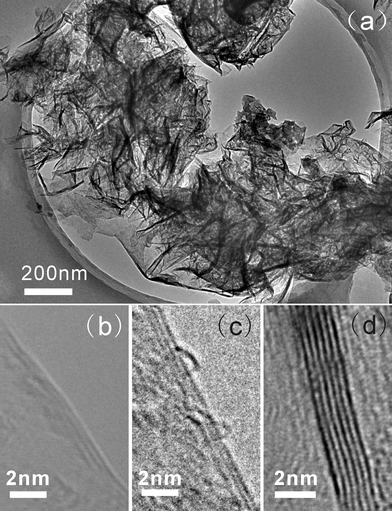 | ||
| Fig. 2 TEM images of the BCN nanosheets prepared at the CH4 flow rate of 1 sccm: (a) Low magnification image. (b–d) High magnification TEM images showing the BCN nanosheets with different atomic layers: (b) 2, (c) 3, and (d) 6. | ||
Fig. 3(a) shows the Raman spectrum of the BCN nanosheets, where two overlapped strong peaks centered at 1360 and 1595 cm−1 and a broad band ranging from 2480 to 3200 cm−1 can be observed. This spectrum is similar to that reported for other BCN materials such as BCN nanotubes,24,25 atomically thin BCN films,17 and BCN nanosheets prepared by solid state reacton.18 The Raman spectra of the BCN materials, including those previously reported and the present one, show similar features to that of carbon.26,27 Up to now, the detailed explanation of the Raman spectra of BCN materials is still unresolved. According to the explanation for carbon materials, the peaks at 1360 and 1595 cm−1 in Fig. 3(a) can be assigned to the D and G band, respectively, and the broad band between 2480 and 3200 cm−1 is assigned to the second-order Raman signals, which can be deconvoluted into two bands centered at 2668 and 2900 cm−1, corresponding to the 2D overtone and D + G combination modes, respectively.24,28 But this explanation seems not to reflect the presence of B and N atoms in the BCN materials. Wu et al.25 measured the Raman spectra of the radially phase separated BCN nanotubes and assigned the peak at 1366 cm−1 to the E2g mode of BN and that at 1585 cm−1 to the E2g mode of graphite. If the BN and carbon are phase separated in the BCN materials this explanation is reasonable. Because the D peak of carbon and the higher frequency E2g mode of hexagonal BN are so close we prefer to think that the peak at 1360 cm−1 is the superimposition of the above two peaks and the peak at 1595 cm−1 can be regarded as the G peak of carbon materials. However, because of the complexity of bonding states in the BCN materials further work is needed to make a conclusion regarding the explanation of the Raman spectra of the BCN materials. EELS measurements were made to determine the chemical structure and composition of the BCN nanosheets. Fig. 3(b) shows the typical EELS spectrum of the BCN nanosheets. Three distinct absorption peaks located at 188, 284 and 401 eV are seen, corresponding to the K-shell ionization edges of B, C, and N, respectively. Their sharp π* peaks and the shapes of σ* peaks indicate that B, C, and N elements are sp2-hybridized, forming graphite-like hexagonal structure.17,29 The quantification of the spectrum in Fig. 3(b) gives the chemical composition of B0.38C0.27N0.35 for the BCN nanosheets prepared at the selected conditions.
 | ||
| Fig. 3 Typical (a) Raman and (b) EELS spectrum of the BCN nanosheets prepared at the CH4 flow rate of 1 sccm. | ||
Electronic structure and optical properties of the BCN nanosheets were investigated by measuring their PL spectra. In order to probe into the effects of the chemical composition on the PL properties of the BCN nanosheets the PL spectra were measured on the samples prepared at the CH4 gas flow rates of 1, 3, 5, and 9 sccm. As shown in Fig. 4, all of the spectra exhibit an intense peak centered at 3.27–3.31 eV (3.27, 3.31, 3.30, and 3.29 eV for the samples prepared at the CH4 flow rates of 1, 3, 5, and 9 sccm, respectively) and multiple emission peaks in the range of 1.9–2.9 eV. It is observed that the emission in 1.9–2.9 eV increases remarkably with increasing the CH4 flow rate, while the emission peaks in the range of 3.27–3.31 eV are relatively stable. As clearly indicated in Fig. 4, at the CH4 flow rate of 1 sccm the 1.9–2.9 eV emission peaks are very weak, even negligible compared with the intense emission at 3.27 eV; but at the CH4 flow rate of 9 sccm the 1.9–2.9 eV emission is comparable to the emission at 3.29 eV. The emission in 1.9–2.9 eV can be logically ascribed to defects. The defect density may increase with increasing the carbon content, resulting in the increase of the emission intensity. The 3.27–3.31 eV emission is likely to be caused by band-to-band transitions across the direct band gap of the samples. Various emission peaks have been reported for the BCN materials with different compositions such as 3.81 eV for BCN,12 2.1 eV for BC2N,30 1.0 eV for B0.34C0.42N0.24,10 and 3.5–4.2 eV for BN–C phase separated BCN nanotubes.25 The difference between the emission peaks in the present work and those in the previous reports is obviously caused by the structural and compositional differences. Interestingly, the emission in the range 3.27–3.31 eV is basically stable with increasing the CH4 flow rate, which seems to be inconsistent with the prediction and observation that the band gap of the BCN materials depends on their composition. However, the structure of the BCN materials is very complicated and both atomic level hybrids of the B, C, and N atoms and phase separated mixtures have been proposed and observed.12,17,25,30 Different emission peaks may arise for similar chemical compositions if the phase compositions are different. In the present case, we think that in the applied conditions a stable BCN phase may form independent of the CH4 flow rate. In our previous reports,31,32,33 where BCN films and nanofibers were prepared by hot-filament CVD from a gas mixture of B2H6–CH4–N2–H2, the PL peaks shifted upwards with increasing the B2H6 flow rate. In the present case, the CH4 flow rate was increased while keeping the BF3 flow rate constant. It is probable that the excessive carbon atoms form a carbon (graphite) phase rather than bonding with the limited B and N atoms, and thus keeping the structure and composition of the BCN phase stable with increasing the CH4 flow rate. But further work is needed to study the detailed mechanism of the PL emission.
 | ||
| Fig. 4 PL spectra of the BCN nanosheets grown at different CH4 flow rates. | ||
In conclusion, BCN nanosheets as thin as a few atomic layers were synthesized by MPCVD. The BCN nanosheets grow with their orientation perpendicular to the substrate surface. The PL spectra of the BCN nanosheets are dependent on their chemical composition and the nanosheets with the composition of B0.38C0.27N0.35 show intense emission at 3.27 eV with very weak defect-related emission. The present BCN nanosheets are promising for applications in nanoelectronics, catalyst supports, and gas adsorption, etc.
Acknowledgements
This work was supported by the NSFC (grant nos. 50972033 and 50572019), the New Century Excellent Talents in University (NCET060343), SRF for ROCS, SEM, and S&T Program of Shenzhen Government.References
- K. S. Novoselov, A. K. Geim, S. V. Morozov, D. Jiang, Y. Zhang, S. V. Dubonos, I. V. Grigorieva and A. A. Firsov, Science, 2004, 306, 666 CrossRef CAS.
- C. N. R. Rao, A. K. Sood, K. S. Subrahmanyam and A. Govindaraj, Angew. Chem., Int. Ed., 2009, 48, 7752 CrossRef CAS.
- A. A. Balandin, S. Ghosh, W. Z. Bao, I. Calizo, D. Teweldebrhan, F. Xiao and C. N. Lau, Nano Lett., 2008, 8, 902 CrossRef CAS.
- A. K. Geim and K. S. Novoselov, Nat. Mater., 2007, 6, 183 CrossRef CAS.
- M. D. Stoller, S. Park, Y. Zhu, J. An and R. S. Ruoff, Nano Lett., 2008, 8, 3498 CrossRef CAS.
- C. Lee, X. Wei, J. W. Kysar and J. Hone, Science, 2008, 321, 385 CrossRef CAS.
- X. L. Li, X. R. Wang, L. Zhang, S. Lee and H. J. Dai, Science, 2008, 319, 1229 CrossRef CAS.
- S. Stankovich, D. A. Dikin, G. H. B. Dommett, K. M. Kohlhaas, E. J. Zimney, E. A. Stach, R. D. Piner, S. T. Nguyen and R. S. Ruoff, Nature, 2006, 442, 282 CrossRef CAS.
- R. Sen, B. C. Satishkumar, A. Govindaraj, K. R. Harikumar, G. Raina, J. P. Zhang, A. K. Cheetham and C. N. R. Rao, Chem. Phys. Lett., 1998, 287, 671 CrossRef CAS.
- J. Yu, J. Ahn, S. F. Yoon, Q. Zhang, Rusli, B. Gan, K. Chew, M. B. Yu, X. D. Bai and E. G. Wang, Appl. Phys. Lett., 2000, 77, 1949 CrossRef CAS.
- W. Q. Han, J. Cumings, X. Huang, K. Bradley and A. Zettl, Chem. Phys. Lett., 2001, 346, 368 CrossRef CAS.
- L. W. Yin, Y. Bando, D. Golberg, A. Gloter, M. S. Li, X. L. Yuan and T. Sekiguchi, J. Am. Chem. Soc., 2005, 127, 16354 CrossRef CAS.
- L. Liao, K. H. Liu, W. L. Wang, X. D. Bai, E. G. Wang, Y. L. Liu, J. C. Li and C. Liu, J. Am. Chem. Soc., 2007, 129, 9562 CrossRef CAS.
- D. Portehault, C. Giordano, C. Gervais, I. Senkovska, S. Kaskel, C. Sanchez and M. Antonietti, Adv. Funct. Mater., 2010, 20, 1827 CrossRef CAS.
- H. Konno, T. Ito, M. Ushiro, K. Fushimi and K. Azumi, J. Power Sources, 2010, 195, 1739 CrossRef CAS.
- J. Yu and E. G. Wang, Appl. Phys. Lett., 1999, 74, 2948 CrossRef CAS.
- L. Ci, L. Song, C. Jin, D. Jariwala, D. Wu, Y. Li, A. Srivastava, Z. F. Wang, K. Storr, L. Balicas, F. Liu and P. M. Ajayan, Nat. Mater., 2010, 9, 430 CrossRef CAS.
- K. Raidongia, A. Nag, K. P. S. S. Hembram, U. V. Waghmare, R. Datta and C. N. R. Rao, Chem.–Eur. J., 2010, 16, 149 CrossRef CAS.
- W. Q. Han, H. G. Yu and Z. X. Liu, Appl. Phys. Lett., 2011, 98, 203112 CrossRef.
- J. C. Meyer, A. K. Geim, M. I. Katsnelson, K. S. Novoselov, T. J. Booth and S. Roth, Nature, 2007, 446, 60 CrossRef CAS.
- J. Yu, L. Qin, Y. F. Hao, S. Y. Kuang, X. D. Bai, Y. M. Chong, W. J. Zhang and E. G. Wang, ACS Nano, 2010, 4, 414 CrossRef CAS.
- L. Qin, J. Yu, M. Y. Li, F. Liu and X. D. Bai, Nanotechnology, 2011, 22, 215602 CrossRef.
- N. G. Shang, P. Papakonstantinou, M. McMullan, M. Chu, A. Stamboulis, A. Potenza, S. S. Dhesi and H. Marchetto, Adv. Funct. Mater., 2008, 18, 3506 CrossRef CAS.
- C. Y. Zhi, X. D. Bai and E. G. Wang, Appl. Phys. Lett., 2002, 80, 3590 CrossRef CAS.
- J. Wu, W. Q. Han, W. Walukiewicz, J. W. Ager III and W. Shan, Nano Lett., 2004, 4, 647 CrossRef CAS.
- F. Tuinstra, J. L. Koenig and J. Chem, Phys., 1970, 53, 1126 CAS.
- R. J. Nemanich and S. A. Solin, Phys. Rev. B, 1979, 20, 392 CrossRef CAS.
- F. Piazza, J. E. Nocua, A. Hidalgo, J. De Jesus, R. Velazquez, B. L. Weiss and G. Morell, Diamond Relat. Mater., 2005, 14, 965 CrossRef CAS.
- M. Terrones, D. Golberg, N. Grobert, T. Seeger, M. Reyes-Reyes, M. Mayne, R. Kamalakaran, P. Dorozhkin, Z.-C. Dong, H. Terrones, M. Ruhle and Y. Bando, Adv. Mater., 2003, 22, 1899 CrossRef.
- M. O. Watanabe, S. Itoh, T. Sasaki and K. Mizushima, Phys. Rev. Lett., 1996, 77, 187 CrossRef CAS.
- J. Yu, E. G. Wang, J. Ahn, S. F. Yoon, Q. Zhang, J. Cui and M. B. Yu, J. Appl. Phys., 2000, 87, 4022 CrossRef CAS.
- X. D. Bai, E. G. Wang and J. Yu, Appl. Phys. Lett., 2000, 77, 67 CrossRef CAS.
- C. Y. Zhi, J. D. Guo, X. D. Bai and E. G. Wang, J. Appl. Phys., 2002, 91, 5325 CrossRef CAS.
| This journal is © The Royal Society of Chemistry 2012 |