Real-time DNA detection using Pt nanoparticle-decorated reduced graphene oxide field-effect transistors
Zongyou
Yin†
a,
Qiyuan
He†
a,
Xiao
Huang
a,
Juan
Zhang
a,
Shixin
Wu
a,
Peng
Chen
ab,
Gang
Lu
a,
Peng
Chen
c,
Qichun
Zhang
a,
Qingyu
Yan
a and
Hua
Zhang
*ab
aSchool of Materials Science and Engineering, Nanyang Technological University, 50 Nanyang Avenue, Singapore 639798. E-mail: hzhang@ntu.edu.sg; hzhang166@yahoo.com; Web: http://www.ntu.edu.sg/home/hzhang Fax: +65 67909081
bCenter for Biomimetic Sensor Science, Nanyang Technological University, 50 Nanyang Drive, Singapore 637553
cSchool of Chemical and Biomedical Engineering, Nanyang Technological University, 70 Nanyang Drive, Singapore 637457
First published on 16th November 2011
Abstract
A large-area, continuous, few-layer reduced graphene oxide (rGO) thin film has been fabricated on a Si/SiO2 wafer using the Langmuir–Blodgett (LB) method followed by thermal reduction. After photochemical reduction of Pt nanoparticles (PtNPs) on rGO, the obtained PtNPs/rGO composite is employed as the conductive channel in a solution-gated field effect transistor (FET), which is then used for real-time detection of hybridization of single-stranded DNA (ssDNA) with high sensitivity (2.4 nM). Such a simple, but effective method for fabrication of rGO-based transistors shows great potential for mass-production of graphene-based electronic biosensors.
Introduction
Graphene,1 a one-atom-thick conjugated carbon sheet, has attracted intense attention due to its unique electrical, mechanical, chemical and physical properties. Graphene has shown potential electronic applications in field effect transistors (FETs),2–8memories,9–12 sensors,7,8,13–16 and photovoltaics.17–22 Meanwhile, owing to its good chemical stability and biocompatibility, graphene has attracted increasing interest in biological studies and biotechnologies, which include electronic and fluorescent biosensors,23–25drug delivery,26 and living cell study.3,27,28 In particular, electronic sensors based on graphene channels, which exhibit a large and homogeneous detection area, have shown promising results in detecting biomolecules7,29,30 and cells3,31 with high sensitivity.Graphene is known to adsorb single-stranded DNA (ssDNA) through the π–π interaction between the hexagonal carbon ring of graphene sheet and the ring structure in nucleic acid.13,32–35 This makes graphene an ideal platform for DNA detection. Although graphene-based fluorescent sensors have been used for DNA detection,23 it mostly relied on the fluorescent label. Electronic DNA sensors based on graphene channels, on the other hand, are label-free and can offer real-time detection that directly reflects the binding of target DNA, which is favoured for practical applications both in vitro and in vivo.
Although graphene has shown great potential in label-free DNA sensing, mass production of graphene with reliable procedures and low cost has not been realized, which restricts the wide applications of graphene. For example, pristine graphene obtained from mechanical cleavage is limited by the low-yield production and lack of controllability in film quality, while chemical vapor deposition (CVD)-grown graphene is compromised by high cost. Therefore, graphene oxide (GO), a water soluble colloidal suspension from chemical exfoliation of graphite, has become a promising alternative.1,36 GO can be chemically or thermally reduced to conductive reduced graphene oxide (rGO). Compared to the pristine graphene or CVD-grown graphene, rGO thin films have offered competitive results as channel materials in various electronic biosensors.3,7,24,26,37 However, the commonly used techniques to fabricate rGO thin films, such as spin-coating, vacuum-filtration, spray deposition and liquid/air-interface based self-assembly, are either difficult to control the film thickness and uniformity or complex in the fabrication process. Recently, Cote et al. reported the deposition of GO sheets on substrates with controllable thickness and flat sheet morphology by using the Langmuir–Blodgett (LB) method.38
In this contribution, we fabricated a large-area, continuous, few layer GO film with controlled thickness by the LB method, which was then reduced with thermal annealing to obtain a conductive rGO thin film. After Pt nanoparticles (PtNPs) were directly synthesized onto rGO sheets by photochemical reduction, the resulting PtNPs/rGO composite was used as a channel material in a solution-gated field-effect transistor (FET). Thiolated probe DNA was attached to the PtNPs on rGO channelvia the Pt–S bonding before the FET was used for real-time, label-free detection of hybridization of target DNA in buffer solution. The calculated detection limit reached around 2.4 nM, indicating the high sensitivity of our PtNPs/rGO based FET DNA sensor.
Results and discussion
Preparation and characterization of PtNP-decorated few-layer rGO films on Si/SiO2 substrates
A large-area, continuous, few-layer GO film was fabricated on a pre-cleaned hydrophilic Si/SiO2 substrate by the LB method38 (Scheme 1A, see the Experimental section for details). As shown in the scanning electron microscopy (SEM) image (Fig. 1A), the size of most GO sheets is in the range of several to 20 μm. The continuous GO film obtained from the LB method is composed of single-layer GO sheets, and folding/stacking induced double- and triple-layer GO sheets (Fig. 1A). Such a method can be applied to many substrates (e.g.SiO2, quartz and polymers) to obtain the wafer-size, continuous, few-layer GO film. The thickness of the obtained GO film is about 1–3 nm, corresponding to the stacking of 1–3 layered GO sheets (Fig. 1B). Subsequently, the few-layer GO film was reduced with the high-temperature annealing in Ar/H2 atmosphere at 1000 °C for 2 h, and the reduced graphene oxide (rGO) film was obtained (Scheme 1B). Such a reduction method enables an environment-friendly and more efficient reduction of GO compared with the chemical reduction by using hydrazine vapor.20,39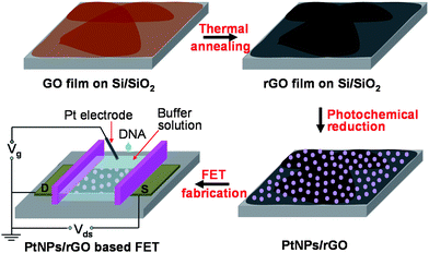 | ||
| Scheme 1 Schematic illustration of fabrication of a solution-gated FET device based on PtNPs/rGO films for DNA detection. | ||
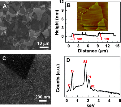 | ||
| Fig. 1 (A) SEM image of GO film on the Si/SiO2 substrate prepared by the LB method. (B) Topographic atomic force microscopy (AFM) image (19 × 19 μm2) and section analysis of GO film on Si/SiO2. (C) SEM image of photochemically synthesized PtNPs on a high-temperature-annealing reduced GO (rGO) film. (D) EDX spectrum of the PtNPs/rGO composite on Si/SiO2. | ||
Recently, GO or rGO has been used as an effective template for synthesis of Ag or Au nanostructures.1,40–42 Herein, Pt nanoparticles (PtNPs) were directly synthesized on the rGO film, referred to as PtNPs/rGO, by immersion of the rGO-coated Si/SiO2 substrate in an ethanolic solution of PtCl42−, followed by light irradiation (Scheme 1C). Previous studies have shown that chloro–platinum complexes (e.g.PtCl62− or PtCl42−) can be photochemically reduced to Pt0 in the presence of alcohols,43,44 which undergo oxidation and provide electrons for Pt reduction. Besides the reaction mentioned above,43,44 the reduction of PtCl42− might also happen due to the different reduction potentials of PtCl42− (+0.775 V vs. the standard hydrogen electrode, SHE)45 and rGO (+0.38 V vs.SHE),46 since the electrons could be donated from the rGO surface. The similar phenomenon has been observed in graphene or rGO templated growth of Au30 and Ag40nanostructures. Consequently, as shown in the SEM image in Fig. 1C, relatively dense PtNPs in the size of ∼10 nm were formed on rGO, which were confirmed by the energy-dispersive X-ray (EDX) spectrum. As shown in Fig. 1D, two peaks at 2.07 and 2.3 keV are attributed to the Mα–Mβ and Mγ peaks of Pt, respectively.47 Note that the detected C is from rGO, and O is mainly from the SiO2 substrate while a very small portion may arise from the incomplete reduction of the rGO film.
Electronic properties of PtNPs/rGO based field-effect transistors (FETs) before and after modification with probe DNA
The fabrication of PtNPs/rGO based solution-gated FETs (Scheme 1D) has been presented in detail in the Experimental section. The electrical properties of the FETs based on the rGO channel and PtNPs/rGO channel were characterized, as shown in Fig. 2A. Similar ambipolar characteristics were observed in both FETs with a broad transition at the Dirac point (∼+0.4 V) and an ON/OFF ratio of ∼2, which is consistent with our previous observation on rGO based FETs.3 The modification of PtNPs on the rGO channel did not result in obvious change of the transconductance as compared with the rGO-based FET (Fig. 2A).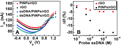 | ||
| Fig. 2 (A) Plot of Idsvs. Vg at Vds = 400 mV for FETs with the channel of rGO, PtNPs/rGO, PtNPs/rGO modified with 10 μM probe DNA (i.e. ssDNA/PtNPs/rGO), and ssDNA/PtNPs/rGO hybridized with 100 nM target DNA (i.e. dsDNA/PtNPs/rGO). (B) Plot of conductance change vs. the concentration of immobilized probe DNA on rGO and PtNPs/rGO based FETs. | ||
The chemical immobilization of thiolated probe DNA onto the PtNP surface was realized through the Pt–S covalent bonding. As shown in Fig. 2A, the immobilization of 10 μM probe DNA on the PtNPs/rGO based FET, referred to as ssDNA/PtNPs/rGO, clearly caused the n-doping effect with a left shift of the Ids–Vg (Ids: drain to source current, Vg: applied gate voltage) characteristic curve. This is in agreement with the previous observation of graphene-based FETs upon adsorption of DNA molecules.30 Hence, a decrease of conductance (current) is anticipated at Vg = 0 V. As shown in Fig. 2B, the FET devices modified with probe DNA showed the decrease of Ids (at Vg = 0 V) with increase of the probe DNA concentration. In a control experiment, the adsorption of probe DNA on the rGO-based FET resulted in a similar trend of current decrease, but the decreased percentage is much smaller compared to that obtained in the PtNPs/rGO based FET (Fig. 2B). Such slight current decrease in the rGO-based FET indicated that there is a small amount of non-specific adsorption of probe DNA on the rGO surface. Several reports have also shown that the ssDNA molecules can be adsorbed on the GO or graphene surface through the π–π interaction.13,30,48,49 However, the more significant decrease of Ids from the PtNPs/rGO channel, compared to the rGO channel, confirmed much more adsorption of thiolated probe DNA on PtNPs/rGO due to the Pt–S bonding. Correspondingly, the conductance change of PtNPs/rGO based FETs induced by the DNA doping effect dominantly arises from the ssDNA adsorbed on PtNPs, instead of the non-specific adsorption of ssDNA on the underneath exposed rGO surface uncovered by PtNPs. In the PtNPs/rGO based FETs, Ids almost stopped decreasing when the concentration of probe DNA exceeded 10 μM (Fig. 2B), indicating that the adsorption of ssDNA on the PtNPs/rGO surface was saturated.
Real-time DNA detection
The PtNPs/rGO based FET, modified with probe DNA, was used to detect the hybridization of target DNA in real time. After the target DNA was added into the sensing chamber containing the phosphate buffered saline (PBS) buffer, Ids was continuously monitored to analyze the hybridization of the added target DNA with the probe DNA anchored on PtNPs. Fig. 3A shows a typical real-time recording of Ids when the target DNA was added with gradually increasing concentration. The adsorption of target DNA due to the hybridization to its complementary probe DNA on PtNPs caused a decrease of Ids. Such decrease of current (conductance) can be explained by the increased n-doping effect30,50 due to the adsorption of target DNA onto the probe DNA-modified PtNPs/rGO channel, i.e. dsDNA/PtNPs/rGO formed. This is confirmed by the Ids–Vg characteristics after addition of 100 nM target DNA (Fig. 2A), which clearly shows a left shift compared with that obtained in the ssDNA/PtNPs/rGO based FET. This result is consistent with the previous reports.30,51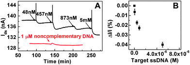 | ||
| Fig. 3 (A) Real-time recording of the hybridization between target DNA and probe DNA immobilized on PtNPs/rGO channels in PBS buffer. Vds = 400 mV. A control experiment result with addition of noncomplementary ssDNA is also plotted (red line). (B) Plot of conductance change vs. concentration of target DNA. | ||
Fig. 3B shows the change of the conductance with the increasing concentration of target DNA. Here, a lowest quantity of 48 nM of target DNA with a signal-to-noise ratio of 60 was demonstrated, giving a detection limit of around 2.4 nM at the signal-to-noise ratio of 3. In a control experiment, the addition of 1 μM noncomplementary DNA into the chamber of the same probe DNA-modified PtNPs/rGO sensor resulted in no obvious change of Ids (Fig. 3A), indicating that the change of the conductance is indeed due to the hybridization between the target DNA and probe DNA instead of the non-specific adsorption of ssDNA on the rGO surface that was not covered by the PtNPs. Moreover, the pre-covered rGO surface by the probe DNA may also prevent such non-specific adsorption of the noncomplementary DNA on its surface.
Conclusions
A large-area, continuous, and few-layer rGO thin film has been prepared on a Si/SiO2 wafer by the LB method followed by thermal reduction. After functionalization of rGO with Pt nanoparticles (PtNPs) by photochemical reduction, the PtNPs/rGO composites have been successfully used in solution-gated FETs for real-time detection of DNA. A calculated DNA detection limit of 2.4 nM is achieved. This simple, but effective fabrication method for the FETs has provided a promising platform for development of graphene-based biosensors.Experimental section
Preparation of few-layer rGO film on Si/SiO2 substrates by the LB method
0.3 mg mL−1 GO aqueous solution was first diluted in methanol at a volume ratio of 1![[thin space (1/6-em)]](https://www.rsc.org/images/entities/char_2009.gif) :5. The GO solution, dispersed in the above mixed solvent (H2O/methanol), was then centrifuged at 8000 rpm for 20 min to remove the small GO sheets. The obtained bottom part of GO solution was re-dispersed into a new mixed solvent of H2O/methanol (v:v = 1:5). This GO solution was further centrifuged at 1500 rpm for 15 min and the bottom precipitate was discarded in order to remove the large GO sheets. Then, the final supernatant, i.e. GO solution, was used to form GO film on Si/SiO2 by the LB method.
:5. The GO solution, dispersed in the above mixed solvent (H2O/methanol), was then centrifuged at 8000 rpm for 20 min to remove the small GO sheets. The obtained bottom part of GO solution was re-dispersed into a new mixed solvent of H2O/methanol (v:v = 1:5). This GO solution was further centrifuged at 1500 rpm for 15 min and the bottom precipitate was discarded in order to remove the large GO sheets. Then, the final supernatant, i.e. GO solution, was used to form GO film on Si/SiO2 by the LB method.
Before the formation of GO film on Si/SiO2, the trough (KSV instruments, Finland) of LB equipment was cleaned thoroughly and then filled with Milli-Q water. GO solution was spread dropwise onto the water surface using a glass syringe. The surface pressure was monitored by a tensiometer, which was targeted at 10 mN m−1 for the GO film coating on Si/SiO2. The target surface pressure was realized and then maintained constant by in situ compression of the two barriers during the LB process. The GO film was transferred onto the pre-cleaned Si/SiO2 substrate by vertically dipping the substrate into the trough (80 mm min−1) and then slowly pulling it up (0.5–1 mm min−1). After that, the GO film on Si/SiO2 was dried at 80 °C for 1 h. To make a large-area, continuous and few-layer GO film on the substrate, a second round of GO deposition, by repeating the aforementioned LB process, was performed. The finally obtained GO film on Si/SiO2 was annealed in the Ar:H2 (30%:70%, v:v) atmosphere at 1000 °C for 2 h to form the rGO film on Si/SiO2.
AFM images were obtained using a Dimension 3100 (Veeco, CA) in tapping mode with a Si tip (Veeco, resonant frequency, 320 kHz; spring constant, 42 N m−1) under ambient conditions with a scanning rate of 1 Hz and a scanning line of 512. SEM image was obtained by a JEOL JSM-7600F field-emission scanning electron microanalyzer (Japan) with an accelerating voltage set at 5 kV and 20 kV, for the capturing of images and EDX determination, respectively.
Synthesis of PtNPs on rGO film coated on Si/SiO2
After 5 mL of 1 mM Na2PtCl4 solution in the mixed H2O/ethanol (v:v = 1:1) solvent was transferred into a transparent glass bottle, a proper-sized Si/SiO2 wafer covered with rGO film was immersed in the solution with the whole wafer leaning on the wall of the bottle. In order to make an efficient and complete reaction for deposition of dense PtNPs on rGO, the light source was introduced to directly face the rGO film on Si/SiO2. Then the bottle was capped and photoirradiated with a 150 W quartz halogen fiber optic illuminator (mode MI-150, Fiber-Lite, USA) at 80% of the lamp power for 25 min. Since there was some heat generated during the reaction process, after reaction, the solution was first cooled down to room temperature and then the obtained sample, i.e.Pt nanoparticles coated rGO film (PtNPs/rGO), was taken out of the bottle. After washing with ethanol and then drying with N2 gas, the sample was ready for fabrication of the field-effect transistor (FET).
Fabrication of FETs
The obtained PtNPs/rGO substrate was defined in 3 × 3 mm2 by scratching away the excess rGO film with a plastic tip by using our previously reported scratching method.7 Therefore, both the length and width of the rGO film were fixed at 3 mm, representing the length and width of the active channel. Silver paste was deposited on both sides of the rGO film to form drain and source electrodes. Silicone rubber was used to insulate both electrodes3,7,8 and define a 2.5 × 2.5 mm2 sensing chamber containing the PBS buffer solution for characterization of solution-gated FETs and the following real-time DNA detection.Immobilization of probe DNA and real-time detection of target DNA
The immobilization of thiolated DNA (probe DNA) was conducted by dropping 20 μL solution of probe DNA (5′ SH-TTT TTT TTT T CAA CCT CAA ACA GAC ACC ACG GT 3′, 100 μM in PBS) on the PtNPs/rGO channel for 4 h and then rinsing with PBS. After the modification of probe DNA, the real-time detection was carried out by addition of the complementary target DNA (5′ C CGT GGT GTC TGT TTG AGG TTG 3′) or 1 μL of 21 μM noncomplementary control DNA (5′ GTT CTT CAA TGA AGT GGG ACG ACA 3′) into the sensing chamber containing 20 μL PBS buffer while the drain–source current was continuously monitored. The concentration was varied by changing the addition of target DNA solution (i.e. 1 μL of 1 μM, 0.9 μL of 10 μM, 1 μL of 10 μM, and 1 μL of 100 μM) into the sensing chamber containing 20 μL PBS buffer to give a final concentration of 48 nM, 457 nM, 873 nM, and 5 μM.Acknowledgements
This work was supported by AcRF Tier 2 (ARC 10/10, no. MOE2010-T2-1-060) from MOE, CREATE program (Nano-materials for Energy and Water Management) from NRF, and New Initiative Fund FY 2010 (M58120031) from NTU in Singapore.Notes and references
- (a) X. Huang, Z. Y. Yin, S. X. Wu, X. Y. Qi, Q. Y. He, Q. C. Zhang, Q. Y. Yan, F. Boey and H. Zhang, Small, 2011, 7, 1876–1902 CrossRef CAS; (b) X. Huang, X. Y. Qi, F. Boey and H. Zhang, Chem. Soc. Rev., 2012 10.1039/c1cs15078b.
- K. S. Novoselov, A. K. Geim, S. V. Morozov, D. Jiang, Y. Zhang, S. V. Dubonos, I. V. Grigorieva and A. A. Firsov, Science, 2004, 306, 666–669 CrossRef CAS.
- Q. Y. He, H. G. Sudibya, Z. Y. Yin, S. X. Wu, H. Li, F. Boey, W. Huang, P. Chen and H. Zhang, ACS Nano, 2010, 4, 3201–3208 CrossRef CAS.
- B. J. Kim, H. Jang, S. K. Lee, B. H. Hong, J. H. Ahn and J. H. Cho, Nano Lett., 2010, 10, 3464–3466 CrossRef CAS.
- Y. Sui and J. Appenzeller, Nano Lett., 2009, 9, 2973–2977 CrossRef CAS.
- B. Li, X. H. Cao, H. G. Ong, J. W. Cheah, X. Z. Zhou, Z. Y. Yin, H. Li, J. Wang, F. Boey, W. Huang and H. Zhang, Adv. Mater., 2010, 22, 3058–3061 CrossRef CAS.
- Q. Y. He, S. X. Wu, S. Gao, X. H. Cao, Z. Y. Yin, H. Li, P. Chen and H. Zhang, ACS Nano, 2011, 5, 5038–5044 CrossRef CAS.
- H. G. Sudibya, Q. Y. He, H. Zhang and P. Chen, ACS Nano, 2011, 5, 1990–1994 CrossRef CAS.
- X. D. Zhuang, Y. Chen, G. Liu, P. P. Li, C. X. Zhu, E. T. Kang, K. G. Noeh, B. Zhang, J. H. Zhu and Y. X. Li, Adv. Mater., 2010, 22, 1731–1735 CrossRef CAS.
- J. Q. Liu, Z. Y. Yin, X. H. Cao, F. Zhao, A. Lin, L. Xie, Q. Fan, F. Boey, H. Zhang and W. Huang, ACS Nano, 2010, 4, 3987–3992 CrossRef CAS.
- S. Myung, J. J. Park, H. Lee, K. S. Kim and S. Hong, Adv. Mater., 2010, 22, 2045–2049 CrossRef CAS.
- Y. Zheng, G. X. Ni, C. T. Toh, M. G. Zeng, S. T. Chen, K. Yao and B. Ozyilmaz, Appl. Phys. Lett., 2009, 94, 163505 CrossRef.
- Z. J. Wang, J. Zhang, P. Chen, X. Z. Zhou, Y. L. Yang, S. X. Wu, L. Niu, Y. Han, L. H. Wang, P. Chen, F. Boey, Q. C. Zhang, B. Liedberg and H. Zhang, Biosens. Bioelectron., 2011, 26, 3881–3886 CrossRef CAS.
- X. H. Cao, Q. Y. He, W. H. Shi, B. Li, Z. Y. Zeng, Y. M. Shi, Q. Y. Yan and H. Zhang, Small, 2011, 7, 1199–1202 CrossRef CAS.
- Z. Wang, X. Zhou, J. Zhang, F. Boey and H. Zhang, J. Phys. Chem. C, 2009, 113, 14071–14075 CAS.
- J. D. Fowler, M. J. Allen, V. C. Tung, Y. Yang, R. B. Kaner and B. H. Weiller, ACS Nano, 2009, 3, 301–306 CrossRef CAS.
- J. L. Song, Z. Y. Yin, Z. J. Yang, P. Amaladass, S. X. Wu, J. Ye, Y. Zhao, W. Q. Deng, H. Zhang and X. W. Liu, Chem.–Eur. J., 2011, 17, 10832–10837 CrossRef CAS.
- Z. Liu, Q. Liu, Y. Huang, Y. Ma, S. Yin, X. Zhang, W. Sun and Y. Chen, Adv. Mater., 2008, 20, 3924–3930 CrossRef CAS.
- N. Yang, J. Zhai, D. Wang, Y. Chen and L. Jiang, ACS Nano, 2010, 4, 887–894 CrossRef CAS.
- Z. Y. Yin, S. X. Wu, X. Z. Zhou, X. Huang, Q. Zhang, F. Boey and H. Zhang, Small, 2010, 6, 307–312 CrossRef CAS.
- V. C. Tung, L. M. Chen, M. J. Allen, J. K. Wassei, K. Nelson, R. B. Kaner and Y. Yang, Nano Lett., 2009, 9, 1949–1955 CrossRef CAS.
- Z. Y. Yin, S. Sun, T. Salim, S. X. Wu, X. Huang, Q. He, Y. M. Lam and H. Zhang, ACS Nano, 2010, 4, 5263–5268 CrossRef CAS.
- S. He, B. Song, D. Li, C. Zhu, W. Qi, Y. Wen, L. Wang, S. Song, H. Fang and C. Fan, Adv. Funct. Mater., 2010, 20, 453–459 CrossRef CAS.
- C. Lu, H. Yang, C. Zhu, X. Chen and G. Chen, Angew. Chem., Int. Ed., 2009, 48, 4785–4787 CrossRef CAS.
- F. Liu, J. Y. Choi and T. S. Seo, Biosens. Bioelectron., 2010, 25, 2361–2365 CrossRef CAS.
- Z. Liu, J. T. Robinson, X. Sun and H. Dai, J. Am. Chem. Soc., 2008, 130, 10876–10877 CrossRef CAS.
- Y. Wang, Z. Li, D. Hu, C. T. Lin, J. Li and Y. Lin, J. Am. Chem. Soc., 2010, 132, 9274–9276 CrossRef CAS.
- S. Agarwal, X. Z. Zhou, F. Ye, Q. Y. He, G. C. K. Chen, J. Soo, F. Boey, H. Zhang and P. Chen, Langmuir, 2010, 26, 2244–2247 CrossRef CAS.
- Y. Ohno, K. Maehashi, Y. Yamashiro and K. Matsumoto, Nano Lett., 2009, 9, 3318–3322 CrossRef CAS.
- X. Dong, Y. Shi, W. Huang, P. Chen and L. J. Li, Adv. Mater., 2010, 22, 1649–1653 CrossRef CAS.
- T. Cohen-Karni, Q. Qing, Q. Li, Y. Fang and C. M. Lieber, Nano Lett., 2010, 10, 1098–1102 CrossRef CAS.
- S. Gowtham, R. H. Scheicher, R. Ahuja, R. Pandey and S. P. Karna, Phys. Rev. B: Condens. Matter Mater. Phys., 2007, 76, 033401 CrossRef.
- J. Antony and S. Grimme, Phys. Chem. Chem. Phys., 2008, 10, 2722–2729 RSC.
- N. Varghese, U. Mogera, A. Govindaraj, A. Das, P. K. Maiti, A. K. Sood and C. R. R. Rao, ChemPhysChem, 2009, 10, 206–210 CrossRef CAS.
- M. Wu, R. Kempaiah, P. J. Huang, V. Maheshwari and J. Liu, Langmuir, 2011, 27, 2731–2738 CrossRef CAS.
- B. Li, G. Lu, X. Z. Zhou, X. H. Cao, F. Boey and H. Zhang, Langmuir, 2009, 25, 10455–10458 CrossRef CAS.
- R. Stine, J. T. Robinson, P. E. Sheehan and C. R. Tamanaha, Adv. Mater., 2010, 22, 5297–5300 CrossRef CAS.
- L. J. Cote, F. Kim and J. Huang, J. Am. Chem. Soc., 2008, 131, 1043–1049 CrossRef.
- H. A. Becerril, J. Mao, Z. Liu, R. M. Stoltenberg, Z. Bao and Y. Chen, ACS Nano, 2008, 2, 463–470 CrossRef CAS.
- X. Z. Zhou, X. Huang, X. Y. Qi, S. X. Wu, C. Xue, F. Y. C. Boey, Q. Y. Yan, P. Chen and H. Zhang, J. Phys. Chem. C, 2009, 113, 10842–10846 CAS.
- (a) X. Huang, S. Z. Li, Y. Z. Huang, S. X. Wu, X. Z. Zhou, S. Z. Li, C. L. Gan, F. Boey, C. A. Mirkin and H. Zhang, Nat. Commun., 2011, 2, 292 CrossRef; (b) X. Huang, H. Li, S. Z. Li, S. X. Wu, F. Boey, J. Ma and H. Zhang, Angew. Chem., Int. Ed. DOI:10.1002/anie.201105850.
- X. Huang, X. Z. Zhou, S. X. Wu, Y. Y. Wei, X. Y. Qi, J. Zhang, F. Boey and H. Zhang, Small, 2010, 6, 513–516 CrossRef CAS.
- R. E. Cameron and A. B. Bocarsly, Inorg. Chem., 1986, 25, 2910–2913 CrossRef CAS.
- R. E. Cameron and A. B. Bocarsly, J. Am. Chem. Soc., 1985, 107, 6116–6117 CrossRef CAS.
- H. C. Choi, M. Shim, S. Bangsaruntip and H. Dai, J. Am. Chem. Soc., 2002, 124, 9058–9059 CrossRef CAS.
- B. S. Kong, J. Geng and H.-T. Jung, Chem. Commun., 2009, 2174–2176 RSC.
- E. U. Donev and J. T. Hastings, Nano Lett., 2009, 9, 2715–2718 CrossRef CAS.
- N. Mohanty and V. Berry, Nano Lett., 2008, 8, 4469–4476 CrossRef CAS.
- Y. Q. Wen, F. F. Xing, S. J. He, S. P. Song, L. H. Wang, Y. T. Long, D. Li and C. H. Fan, Chem. Commun., 2010, 46, 2596–2598 RSC.
- M. Zheng, A. Jagota, E. D. Semke, B. A. Diner, R. S. McLean, S. R. Lustig, R. E. Richardson and N. G. Tassi, Nat. Mater., 2003, 2, 338–342 CrossRef CAS.
- X. W. Tang, S. Bansaruntip, N. Nakayama, E. Yenilmez, Y. L. Chang and Q. Wang, Nano Lett., 2006, 6, 1632–1636 CrossRef CAS.
Footnote |
| † These authors contribute equally to this work. |
| This journal is © The Royal Society of Chemistry 2012 |