DOI:
10.1039/C1NR10856E
(Paper)
Nanoscale, 2012,
4, 194-205
Probing the morphology-device relation of Fe2O3 nanostructures towards photovoltaic and sensing applications†
Received
18th July 2011
, Accepted 6th October 2011
First published on 10th November 2011
Abstract
A lot of research on nanomaterials has been carried out in recent years. However, there is still a lack of nanostructures that have a combination of superior properties; both efficient electron transport and high surface area. Here, the authors have tried to develop hybrid α-Fe2O3 flower-like morphology which exhibits both superior electron transport and high surface area. Intrigued by the unique properties of Fe2O3 at the nanoscale and its abundance in nature, we have demonstrated a facile template-free solution based synthesis of hybrid α-Fe2O3 comprising nanopetals nucleating radially from a 3D core. Due to its simplicity, the synthesis process can be easily reproduced and scaled up. We carried out in-depth studies on gas sensing and dye-sensitized solar cell (DSSC) device characterization so as to gain an understanding of how surface area and transport properties are affected by variation in morphology. The hybrid α-Fe2O3 nanostructures are studied as potential candidates for gas sensors and for the first time as a working electrode for DSSC.
1. Introduction
Metal oxides are a topic of intense research due to their potential use in the development of electronic devices. Many exciting properties emerge when the spatial dimensions of these materials are reduced to the nanoscale. Hence, over the years a large number of metal oxides with complex structures have been successfully synthesized.1–5 Among these, much attention has been focused on hematite (α-Fe2O3) nanostructures because of their various applications.6–11 It is an abundant, stable and environmentally friendly n-type semiconductor with a band gap of 2.2 eV, sufficient to utilize ∼40% of the sunlight. α-Fe2O3 is the most frequently occurring polymorph with a rhombohedral–hexagonal structure. The α-Fe2O3 lattice is composed of alternating iron bi-layers with oxygen layers in parallel to a (001) basal plane. Various shapes and dimensions of α-Fe2O3 nanostructures are available such as nanowires,12nanorods,13nanotubes,14 hollow fibers,15 nanorings16 and cubes.17Fe2O3 has been widely used as catalyst,18,19 photocatalyst20 and for hydrogen production by photoelectrochemical water splitting.21 Nanostructured Fe2O3 has been successfully used as the anode material for lithium-ion batteries.22 The physical and optical properties of α-Fe2O3 have been investigated in depth,23–25 but the transport properties have been limited to electrical conductivity. α-Fe2O3, however, suffers from a short excited state lifetime (∼10 ps) and a poor minority charge carrier mobility (0.2 cm2 V−1 s−1), which limits the efficiency of the devices. One way to overcome these limitations could be through control of morphology, size and porosity of hematite nanostructures. By modifying the structure of α-Fe2O3 Jain et al.22 could enhance the electrochemical properties. High surface area hollow spheres of α-Fe2O3 showed much higher photocatalytic activity compared to their bulk counterparts as reported by Yu et al.26
α-Fe2O3 is an attractive material for gas sensing. However, pure bulk α-Fe2O3 has little to offer for gas sensing applications due to the high operating temperatures required (up to 1000 °C).27 While doping with Al2O3 can help to bring down the operating temperature,28 the use of nanostructured materials promises gas sensing properties at low temperatures.29,30 Moreover, previous studies have showed the importance of high surface area and hierarchical structures for sensing applications.31 High surface area mesoporous α-Fe2O3 structures synthesized by Mao et al.32 and Hao et al.33 have shown good sensing properties for formaldehyde gas and ethanol respectively. Recently, sea-urchin like α-Fe2O3 nanostructures by Zhang et al.,34 three-dimensional superstructures assembled with one-dimensional nanorods, attracted much attention for gas sensing. The large specific surface area and modified electronic properties of these nanostructures are believed to provide numerous active sites for interaction with the analyte gas, resulting in excellent gas sensing behavior even at room temperature.35
After almost 20 years, the efficiencies of DSSCs remain just slightly over 11%.36 It has become apparent that to further enhance the conversion of solar energy into usable electrical power, a material and morphology-based paradigm shift is required. Three-dimensional (3D) nanoparticles have been extensively employed in DSSCs due to a combination of optical transparency and large surface area. However, nanoparticle based DSSCs have the primary weakness of a small diffusion coefficient (D). The electron transport phenomenon in DSSCs is a combination of trapping and de-trapping mechanisms, which are highly dependent on the Fermi level. A typical DSSC made with TiO2 nanoparticles37 shows a diffusion coefficient value of the order of 10−4 cm2 s−1. In order to overcome the apparent limitation of nanoparticles, one-dimensional nanorods and nanotubes are introduced.38,39 The appreciable increase in the diffusion coefficient of nanorods and nanotubes comes from an increased diffusion length (L), thus benefiting charge separation and transport. Compared to 3D nanoparticles, the nanorod morphology lacks a high surface area, significantly decreasing the photocurrent density and therefore limiting the conversion efficiency.38 Hybrid nanostructures have recently emerged as a promising candidate for DSSCs, as they can combine good dye adsorption with better electron transport properties. Achieving a high dye adsorption is possible on a 3D spherical surface, while the presence of a 1D nanostructure can direct the electron transport. A hybrid combination of TiO2 nanowires with P25 nanoparticles in a DSSC achieved a 6.01% solar conversion efficiency, which is 60% higher than DSSCs based on only TiO2 nanowires.40 A 7.12% conversion efficiency is recorded when TiO2 nanorods (∼20 nm diameter) are used in conjunction with P25 nanoparticles.41 The efficiency of ZnO based DSSCs is also improved using hybrid structures.42
In this work, a hybrid α-Fe2O3 flower like morphology is synthesized to achieve a high surface area with a high diffusion coefficient for better electron transport. A simple and reproducible solution route is used to synthesize the nanostructures. An abundance of Fe2O3 in nature and an economical solution based method make this work very attractive for fabricating cheap devices. The performance of devices is investigated for different morphologies of α-Fe2O3 nanostructures, through characterization of the microstructure, electronic and optical properties. Room temperature gas sensing and the possibility of using α-Fe2O3 as a new electrode material for dye sensitized solar cells are explored. To the best of our knowledge the photovoltaic properties of Fe2O3 in DSSCs have not been reported so far. The performance of the devices is evaluated based on the surface area, grain boundaries and diffusion coefficients characteristics. The findings on probing the effect of hybrid nanostructures on various properties are of great importance to surface dominated applications.
2. Experimental
2.1 Preparation of nanoflowers
In a typical experiment, 2 mmol iron chloride (FeCl3·6H2O) and 2 mmol sodium sulfate (Na2SO4) are added into 40 mL deionized water and stirred until totally dissolved. The solution is heated in an autoclave at 120 °C for 6 h and then cooled to room temperature. The products are collected by centrifugation and washed with de-ionized (DI) water and absolute ethanol several times and later dried in air at 60 °C for 12 h. The as-prepared FeOOH powder is annealed in air at 400 °C for 2 h with a ramping rate of 1 °C min−1 to convert to Fe2O3. Various samples with different amounts of iron chloride hexahydrate ranging from 0.04 to 1 mM are prepared.
FeOOH powder and polyethylene glycol (PEG) in a 1![[thin space (1/6-em)]](https://www.rsc.org/images/entities/char_2009.gif) :1 mass ratio are mixed with absolute ethanol to obtain a fine paste of appropriate consistency. The paste is then spread on a microscope glass slide by the “doctor blade” technique to form a film of 5–10 μm thickness. Only one layer of scotch tape (∼40 μm thickness) is used for all the devices. The film is allowed to dry in ambient conditions before heating at 400 °C for 2 h in air. A two-terminal resistor device is made by attaching copper wires to the annealed Fe2O3 film with silver paint (RS 186–3600).
:1 mass ratio are mixed with absolute ethanol to obtain a fine paste of appropriate consistency. The paste is then spread on a microscope glass slide by the “doctor blade” technique to form a film of 5–10 μm thickness. Only one layer of scotch tape (∼40 μm thickness) is used for all the devices. The film is allowed to dry in ambient conditions before heating at 400 °C for 2 h in air. A two-terminal resistor device is made by attaching copper wires to the annealed Fe2O3 film with silver paint (RS 186–3600).
2.3
Dye sensitized solar cell assembly
FeOOH powder is converted into a fine paste using DI water without any binder, and then spread on fluorine doped tin oxide (FTO) glass (resistivity of 15 Ω sq−1) by the “doctor blade” technique (cell area of 0.25 cm2). The film is allowed to dry in ambient conditions before heating at 400 °C for 2 h in air. To make the dye sensitized solar cell (DSSC), the film is immersed in an ethanol solution containing 0.3 mM Ru-dye, (cis-dithiocyanate-N,N′-bis(4-carboxylate-4-tetrabutylammoniumcarboxylate-2,2′-bipyridine) ruthenium(II) (known as N719, Solaronix), for 24 h at room temperature. Subsequently, the films are rinsed with ethanol. The redox electrolyte is prepared with 0.1 M LiI, 0.05 M I2, 0.6 M 1,2-dimethyl-3-propylimidazolium iodide, and 0.5 M 4-tert-butylpyridine in acetonitrile. The electrolyte is injected through the hole in a platinized counter electrode, and the hole is sealed with hot-melt Surlyn (Solaronix) film. 0.04 (D1) and 1 mM (D2) concentration of FeCl3 is used to make the working electrode for the DSSC. It is to be noted that the powder containing 1 mM concentration of FeCl3 is ball milled to obtain a random array of nanopetals. The process of ball milling the 1 mM sample does not change its physicochemical properties and surface area.
2.4 Analysis techniques
A JEOL-2100 high-resolution transmission electron microscope (HRTEM) with an accelerating voltage of 200 kV, along with a selected area electron diffraction (SAED) pattern, and a JEOL FEG JSM 6700 F field-emission scanning electron microscope (FESEM) operating at 10 kV were used to study the morphology of the samples. The film thicknesses were measured using Ambios Technology XP 200 profilometer. Structural characterization of the synthesized films was performed using Philips X-ray diffractometer (XRD) with Cu-Kα radiation. Raman spectroscopy was measured using a Renishaw Ramascope 2000 system with an Olympus microscope attachment and a 514.5 nm laser used as the excitation source. Surface area and porosity information was extracted by Brunauer–Emmett–Teller (BET) measurements using Quantachrome Nova 1200 with N2 as the adsorbate at liquid nitrogen temperature. The optical properties and amount of dye absorbed on the iron oxide film was estimated using a UV-vis spectrophotometer (UV-1800 Shimadzu). The samples for UV-vis measurements were prepared by dip coating FTO glass in 20 mL solution of iron oxide in ethanol. A home-made gas sensing system was used for hydrogen sensing experiments. Details of the setup can be found elsewhere.31 Electrical leads from the sample were connected via an electrical feed-through to an external source-meter (Keithley 4200 SCS). The photocurrent–voltage of the samples was measured with AM1.5 solar simulator (Newport Inst., model 91160A) with an AM filter (81088A). A 150 W Xe lamp was used as the light source. The performance of the solar cells was measured at 25 °C with a sourcemeter (Keithley 2420) and Newport IV test station software. The light intensity corresponding to AM 1.5 (100 mW cm−2) was calibrated using a standard silicon solar cell (Oriel, SRC-1000-TC). The lamp provides uniform illumination in the area of 10 × 10 cm2. Incident photon-to-collected-electron conversion efficiency (IPCE) spectra were measured with a spectral resolution of 5 nm using a 300 W xenon lamp and a grating monochromator equipped with order sorting filters (Newport/Oriel). The incident photon flux was determined using a calibrated silicon photodiode (Newport/Oriel). Photocurrent measurements were made using an auto ranging current amplifier (Newport/Oriel). The control of the monochromator and recording of photocurrent spectra were performed using the TRACQ Basic software (Newport). Electron diffusion coefficients of the films were measured by electrochemical impedance spectroscopy (EIS), which was recorded with a pontentiostat PGSTAT 302N (Autolab, Eco Chemie, The Netherlands) under an illumination of 100 mWcm−2. The frequency range was varied from 10 Hz to 1 MHz and the magnitude of the alternating signal was 0.35 V.
3. Results and discussion
3.1 Characterization of hybrid α-Fe2O3 nanostructures
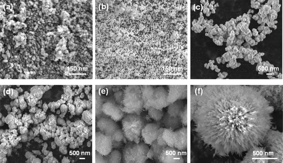
Fig. 1 depicts top view SEM images of a 0.04 mM sample with a flower like morphology. The film is composed of a bundle of nanoflowers (Fig. 1a). The morphology is almost spherical in shape and uniform throughout the sample (Fig. 1b). At high magnification, it can be seen that the film is an interconnected network of large petal like structures originating from the core (Fig. 1c). The average diameter is about 1 μm with a petal thickness of about 50 nm. A closer observation reveals that a few of the nanoflowers are hollow (Fig. 1d). Other researchers have also reported such hollow structures among other morphologies.34,43,44 Dissolution of the core in the reacting solution is postulated to be one of the possibilities. However, the exact mechanism of formation was unclear. The 0.04 mM sample is calcined in air at 400 °C for 2 h. Calcination does not change the overall morphology of the nanoflowers (Fig. 1e and f). The size and texture of the nanoflowers remains almost the same, as confirmed by SEM. The TEM images of nanoflowers (Fig. 2a and b) clearly depict closely packed petals, which agree with the SEM images. The petals of the nanoflower are straight and have a relatively uniform thickness (Fig. 2c). However, TEM image of the petals reveal that some of them may have been disjointed or misaligned during the process of calcination (Fig. 2d).
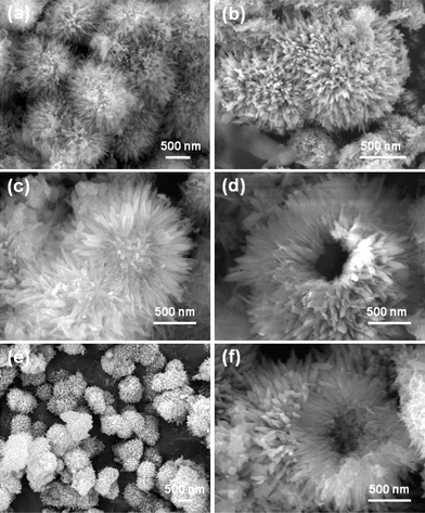 |
| | Fig. 1
FESEM images at (a), (b) low magnification and (c), (d) high magnification of α-FeOOH nanoflowers. (e) and (f) α-Fe2O3 nanoflowers after calcination at 400 °C. | |
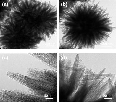 |
| | Fig. 2
TEM images of (a), (b) nanoflowers and (c), (d) petal like structures originating from the nanoflowers. | |
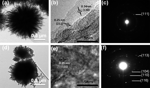
A high resolution TEM (HRTEM) image taken from an as prepared α-FeOOH sample is shown in Fig. 3b. The lattice fringes are visible with a spacing of 0.25 nm and 0.34 nm corresponding to (211) and (130) planes of α-FeOOH respectively. The corresponding SAED pattern (Fig. 3c) of the as prepared sample is not very sharp, representing the almost amorphous nature of the nanoflowers. Upon calcination, the lattice fringe spacing being determined is 0.25 nm (Fig. 3e), corresponding to the (110) lattice plane of α-Fe2O3. The nanoflowers are polycrystalline as seen in SAED data (Fig. 3f).
The ferric solution processed at 120 °C does not yield the hematite phase directly. The XRD analysis (Fig. 4a) identifies the phase of the product to be goethite (α-FeOOH) [JCPDS No: 29-0713] and akaganeite (β-FeOOH) [JCPDS No: 34-1266]. Hence the final phase of the 0.04 mM unannealed sample is composed of a mixture of α- and β-FeOOH. The nanoflowers seem to be polycrystalline in nature before calcination. The approximate crystallite size of the sample is calculated using Scherrer's formula.45 It is calculated to be approximately 0.9 μm, which is close to the value estimated by SEM. A phase change occurs on calcination at 400 °C of the goethite structures, as detected by XRD (Fig. 4b). All peaks are indexed to the rhombohedral phase of hematite [JCPDS No: 89-2810]. The strong and sharp peaks indicate that calcined Fe2O3 powder is highly crystalline. The crystallite size of the calcined nanoflowers is estimated to be 0.6 μm. The results agree well with the SAED data.
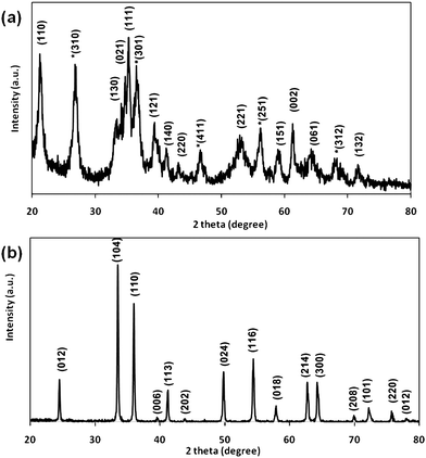 |
| | Fig. 4
XRD pattern of (a) as-obtained α-FeOOH and (b) α-Fe2O3 nanoflowers. | |
α-Fe2O3 is an extrinsic semiconductor with an indirect band gap of 2.2 eV, but a direct band gap has also been reported.46,47UV-vis measurements are employed to deduce the band gap of α-Fe2O3 films. The films prepared of α-Fe2O3 are red-brown and semi-transparent. The thickness is measured to be approximately 1.5 μm. The onset of absorption is revealed to be at around 2 eV in the UV-vis absorption spectrum of Fig. 5a. The transmittance spectrum of the film is shown in Fig. 5b. The average transmittance is found to be about 60% in the visible region. The nature and onset of the electronic transitions can be estimated using the following equation.
where
α is the absorption coefficient,
hν is the
photon energy and
Eg is the band gap energy.
Ao and
m are constants and depend on the type of electronic transition, where
m takes the value of ½ for direct and 2 for indirect band gap transitions. To establish the type of band-to-band transition in the α-Fe
2O
3 samples, the absorption data is fitted to
eqn (1) for both indirect and direct band gap transitions.
Fig. 5c shows the (
αhν)
1/2versusphoton energy plot for an indirect transition and
Fig. 5d shows the (
αhν)
2versusphoton energy for a direct transition. The approximate value of the band gap
Eg is calculated by extrapolating the
photon energy to
αhν = 0. The extrapolation yields an
Eg value of 2.18 eV for indirect and
Eg = 3.46 eV for direct transition. The estimated values are similar to the ones reported in the literature.
47,48 The indirect band gap allows absorption in the UV and the blue part of the visible light region, which gives α-Fe
2O
3 its reddish-brown color. For direct band gap semiconductors, electronic transition from the valence band to the conduction band is electrical dipole allowed. The electronic absorption as well as emission is usually strong for such semiconductors. For indirect band gap semiconductors, the valence band to the conduction band electronic transition is electrical dipole forbidden and the transition is phonon assisted,
i.e., both energy and momentum of the electron–hole pair are changed in the transition. Both their absorption and emission are weaker compared to those of direct band gap semiconductors, since they involve a change in momentum. Hence a direct band gap transition would result in a more efficient absorption of solar energy and therefore much better photovoltaic devices. This might be the research direction for use of α-Fe
2O
3 as an efficient photovoltaic material.
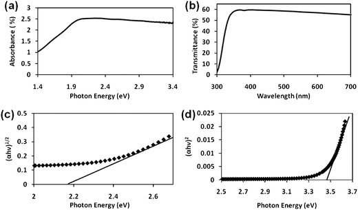 |
| | Fig. 5 (a) Absorption and (b) transmission spectra of the 0.04 mM sample, (c) plot of (αhν)1/2versusphoton energy for an indirect transition and (d) plot of (αhν)2versusphoton energy for indirect transition. | |
3.2
Growth mechanism of hybrid α-Fe2O3 nanostructures
Time dependent experiments are carried out to understand the growth mechanism of the α-FeOOH nanoflowers. The samples collected from reacting the solution mixture at different time intervals during the growth process are observed by SEM. Fig. 6a shows the growth obtained after 30 min with 0.04 mM of FeCl3. Aggregates of solids can be clearly observed. With increased reaction time to 1 h, more growth can be seen (Fig. 6b). The average particle size as estimated from SEM is approximately 100 nm. For the growth times of 2 and 3 h the particles increase in size (∼400 nm) and tend to agglomerate together (Fig. 6c and d). Assembly of 3D structures can be observed when the reaction time reaches 4 h (Fig. 6e). However, at this time the structures are of varying shapes and sizes. At 6 h reaction time, an almost spherical nanoflower morphology can be obtained (Fig. 6f). The authors have also carried out TEM analysis on the time dependent experiments to further investigate the growth mechanism (ESI S1).† On the basis of the time dependent experiments, the α-Fe2O3 nanoflowers are grown via aggregation of nanoparticles followed by nucleation and growth of nanoneedles. In the initial stage, primary α-FeOOH nanoparticles are formed through the hydrolyzation of Fe3+, which serve as the nuclei in the growth process. In the work reported, the presence of Na2SO4 is believed to play a crucial role for the formation of the unique self-assembled structures. It is well known that the aggregation process involves the formation of larger nanoparticles by reducing the interfacial energy of the smaller particles. However, the interaction between unprotected building units is generally not suitable to form stable and uniform microstructures.48 The presence of Na2SO4 provides the necessary strong surface protection to form flower like structures.48 The sulphate ions serve as ligands to Fe3+, and may adsorb on the facets parallel to the c-axis of α-FeOOH nuclei.49 The nanoneedle gradually evolved into 3D flower-like superstructures through oriented attachment to reduce the surface energy. It is speculated that the flower like structures form because bidentate (Fe–O–SO2–O–Fe) type structures are formed between the nanoneedles.49
 |
| | Fig. 6
FESEM images of the product obtained after growth at 120 °C for (a) 0.5 h, (b) 1 h, (c) 2 h, (d) 3 h, (e) 4 h and (f) 6 h. | |
3.3 Effect of FeCl3 concentration on the morphology
The effect of FeCl3 dosage on the final morphology of the product is investigated. The amount of Na2SO4, DI water and other experimental conditions are kept constant. The reaction mixture for growing nanoflowers contains Fe3+ ions from ferric chloride and SO42− ions from sodium sulphate. The ratio of these ions in solution will determine the reaction rate and hence the final morphology. Fig. 7a is the SEM image of the product obtained with 0.12 mM FeCl3 as the dosage. 0.12 mM dosage yields an almost spherical nanoflower like morphology. However, no hollow structures could be observed as with the 0.04 mM concentration. On the contrary the nanoflowers have a solid core as revealed by the SEM image of a broken nanoflower (Fig. 7b). The nanoflower morphology is conserved until the concentration of FeCl3 reaches 0.4 mM (Fig. 7c and d). When the concentration is increased to 0.8 mM (higher concentration of Fe3+ ions) the spherical shape of the nanoflower starts to give way (Fig. 7e). The nanoflowers are no longer spherical and nanorods are disoriented (Fig. 7f). Also the nanorods grow longer and wider. When the Fe3+ ion concentration is further increased in the reacting solution (1 mM), the flower like morphology is completely absent (Fig. 7g). The final product at 1 mM is composed of needle like palates, which tend to originate from the center (Fig. 7h). The needles are sparse and wider in size. The change in morphology with dosage of FeCl3 is also confirmed by TEM. The spherical nanoflower morphology at 0.12 mM concentration and disoriented nanorod formation at 1 mM is clearly visible in TEM images (ESI S2).† With increasing FeCl3 concentration, the nanorods seem to grow in size. For the 0.12 mM solution, the range of the length and width of the petals is 0.8–1 μm and 50–70 nm respectively. The petal shaped structures grow 1.5 μm in length and 90–130 nm in width when the concentration reaches 1 mM. TEM imaging brings out the difference in nanorod dimension for 0.12 and 1 mM samples (ESI S1).†
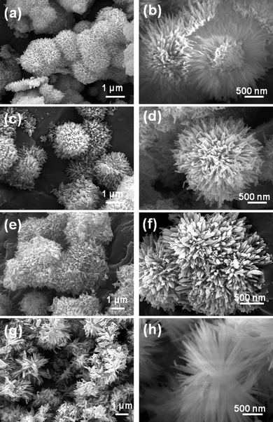 |
| | Fig. 7
SEM images of samples with various FeCl3 concentrations: (a, b) 0.04 mM, (c, d) 0.12 mM, (e, f) 0.4 mM and (g, h) 1 mM. | |
Zeng et al.50 previously studied the effect of the SO42− ion concentration on the morphology of the product. They observed that with a low SO42− ion concentration, an urchin like morphology is obtained, but with higher SO42− concentration, the reaction rate becomes faster and only nanoparticles are formed. It is well established that a prerequisite for obtaining controlled 3D growth is separation of the nucleation and growth process. This separation is absent when the amount of SO42− ions increases in the solution. Combining the knowledge from the two studies (Zeng et al. and this work) it can be safely inferred that if the amount of Fe3+ ions is higher, the reaction speed tends to slow down, thus leading to oriented 3D growth. Hence, a spherical nanoflower morphology is obtained. If the amount of Fe3+ ions is increased (as for 0.8 and 1 mM samples) needle like petals are formed. At this concentration there is no clear boundary separating the nucleation and growth process. The aggregation of nanoparticles may be absent leading to core-less structures with only petals growing in all directions (Fig. 7h).
Table 1 summarizes the various parameters obtained from BET characterization for the different α-Fe2O3 samples. The specific surface area of the sample made from 0.04 mM FeCl3 is found to be the highest (∼109 m2 g−1). As the FeCl3 concentration is increased in the reacting solution, the surface area tends to decrease. This could be due to the formation of large and compact structures leading to a reduction of the surface area to volume ratio. A high surface area is desired for a good amount of dye to be chemisorbed for DSSCs.51 BJH analysis shows that there is not much change in the pore size. However, the pore volume shows a drastic decrease as the FeCl3 concentration is increased. For a 0.04 mM sample with a nanoflower morphology, the pore volume is highest (∼0.27 cc g−1), but it decreases to 0.05 cc g−1 for the 1 mM sample with a disordered array of petal shaped structures. As discussed earlier, core formation is absent for the 1 mM sample. The decreasing pore volume corresponds to the decreasing core size of the nanoflowers with increasing FeCl3 dosage. This tends to indicate that the core of the nanoflowers is porous in nature. The core of the nanoflowers may be composed of aggregates of smaller particles contributing towards the pore volume. This also explains the high surface area for the 0.04 mM sample. Fig. 8 reveals N2 adsorption–desorption isotherms for all the samples. The 0.04 and 0.12 mM products exhibit type IV nitrogen isotherms while 0.4 and 1 mM samples exhibit type III isotherm. The type III isotherm has adsorption and desorption branches of the isotherm that coincide, since no adsorption–desorption hysteresis is displayed, indicating a non-porous material. On the other hand, adsorption on 0.04 and 0.12 mM samples proceeds via multilayer adsorption followed by capillary condensation (type IV isotherm). The adsorption process is initially similar for both these samples, but at higher pressures the amount adsorbed rises for the 0.04 mM morphology due to the capillary condensation in pores. Capillary condensation and evaporation do not take place at the same pressure, thus leading to the formation of a hysteresis loop in the range of 0.6–1.0 P/Po. Monolayer adsorption for the sample containing 0.04 mM FeCl3 is completed at a relative pressure of 0.61. However, the monolayer adsorption for 0.12 mM sample is not completed until it reaches a relative pressure of 0.65. This indicates that the 0.04 mM sample possesses a slightly smaller pore size than the 0.12 mM sample.
Table 1 BET results for different samples of α-Fe2O3
| Sample |
Surface Area (m2 g−1) |
Pore size (nm) |
Pore Volume (cc g−1) |
| 0.04 mM |
109 |
25 |
0.27 |
| 0.12 mM |
75 |
30 |
0.15 |
| 0.4 mM |
59 |
34 |
0.08 |
| 0.8 mM |
55 |
29 |
0.07 |
| 1 mM |
30 |
25 |
0.05 |
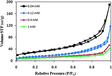 |
| | Fig. 8
Nitrogen adsorption–desorption isotherms at 77 K for nanoflowers produced using different FeCl3 concentrations. | |
3.4 Gas sensing performance of Fe2O3
The as-synthesized α-Fe2O3 nanoflowers are found to be highly sensitive to hydrogen gas at room temperature. This is likely due to the large surface area and modified electronic properties on the surface of the nanoflowers.52,53Hydrogen sensing measurement of a two-terminal film resistor device is carried out by subjecting the device to periodic intervals of clean dry air (CDA) and hydrogen gas at various concentrations at room temperature. The variation of the resistance of a device made from the 0.04 mM sample is shown in Fig. 9a, where Ra and Rg are the resistance of the device in air and hydrogen respectively. Sensitivity of the device is defined as the ratio of the resistance in air and hydrogen, Ra/Rg. As-synthesized α-Fe2O3 nanoflowers are n-type semiconductors due to their intrinsic defect states such as oxygen vacancies. Interaction with the ambient air leaves oxygen molecules adsorbed onto the surface of the nanoflowers:| | | O2(g) ↔ O2 (ad). | (2) |
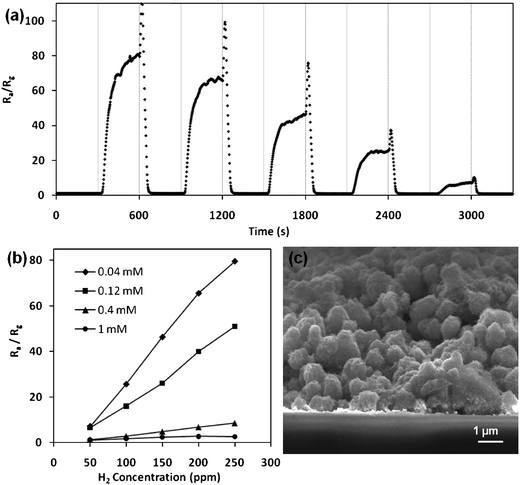 |
| | Fig. 9 (a) Electrical response of the 2-terminal resistor film device to periodic cycles of clean dry air (CDA) and hydrogen gas at various concentrations for the 0.04 mM sample, (b) sensitivity of hydrogen sensor devices fabricated with different dosages of FeCl3 precursors and (c) cross-sectional SEM of the film of inter-connected network of Fe2O3 nanoflowers. | |
The physisorbed oxygen lures electrons from the conduction band of the Fe2O3 nanoflowers to form chemisorbed oxygen species of, O−, O2− and O2−, the latter being favorably chemisorbed at room temperature:
| | | O2(ad) + e− → O2−(ad). | (3) |
The trapping of electrons by the oxygen adsorbate results in an electron-depleted space charge region at the surface of the nanoflowers. This increases the resistance of the interlinked network of nanoflowers due to the surface potential barrier formed in the space charge region, inhibiting electron flow across the grain boundaries. In the presence of hydrogen gas, chemisorbed oxygen ions are reduced to release electrons to the conduction band of the Fe2O3 surface
| | | 2H2 + O2−(ad) → 2H2O + e−, | (4) |
This results in an increase in conductivity. In addition, the reduction reaction decreases the surface density of the oxygen adsorbate, leading to a reduction in the width of the depletion region and the height of the surface potential barrier, thus resulting in the decrease in the resistance of the sensor.20 Excellent sensing behavior of the sensor fabricated from the 0.04 mM sample is observed with an 80-fold drop in resistance when subjected to 250 ppm of hydrogen for 5 min as shown in Fig. 9b. The device is still highly sensitive to 50 ppm of hydrogen (Ra/Rg = 7.1), with the lower limit here bound by the experimental setup. We note that the performance of our sensor excels against α-Fe2O3 nanotubes devices fabricated by Chen et al.53 (Ra/Rg = 2.3 at 50 ppm hydrogen). This is probably due to the higher surface area of nanoflowers (∼109 m2 g−1) compared to the nanotubes (45 m2 g−1). Similar hydrogen sensing measurements are carried out on devices fabricated from 0.12, 0.4 and 1mM samples and the results are summarized in Fig. 9b. The lower sensitivity of the devices made from higher dosages of the FeCl3 precursor is expected due to the lower surface area, corresponding to the BET analysis. It is clearly visible that as the morphology shifts from a hybrid quasi-3D (0.04 mM) to disordered nanorods without a core (1 mM), the surface area drops, thus decreasing the sensitivity of the device. It is noteworthy that the nanoflower morphology is intact for the samples made by the “doctor-blade” method, as shown in a cross-sectional SEM image (Fig. 9c). The current flowing through the sensor may be split between surface and bulk paths, but it must go through two adjacent surface regions during transition from one grain to the other. Thus, there is at least one region where whole sensor conductivity is governed by chemisorption-induced space charge modulation. Hence, at least three parameters could affect conductance: (1) surface area, (2) amount of adsorbed species, and (3) density of grain boundaries. It is clear that the large surface area of hybrid quasi-3D nanoflowers makes them highly sensitive and efficient sensors. The effect of grain boundaries is dealt with later in section 3.5.
3.5 Photovoltaic performance of Fe2O3
Depleting fossil fuels and climate change have sparked intense interest in solar energy harvesting. The focus of the research community is to fabricate high efficiency photovoltaics from low cost and environmental friendly semiconductors. Iron oxide makes up a big portion of the earth's crust and that makes it an attractive candidate for low cost photovoltaics. However, Fe2O3 has not been exploited for photoconversion due to poor charge carrier mobility. This work demonstrates that the answer to this problem may lie in ordered quasi-3D nanostructures with a high surface area. Fig. 10a depicts J–V characteristics of the DSSC made from 0.04 and 1 mM FeCl3 concentrations, named D1 and D2 respectively. A concentration of 0.04 mM is chosen to make the photoanode because the sample possessed a high surface area (∼109 m2 g−1), while a 1 mM sample depicts the 1D nanorod arrangement. Under direct illumination, D1 has a short-circuit current density (Jsc) of around 4.3 mA cm−2, accompanied by an open-circuit voltage (Voc) of 0.6 V and a fill factor (FF) of 63.5%. On the other hand, the DSSC made from the ball milled 1 mM powder shows a poorer performance. The reported values for the D2 cell are: 2.7 mA cm−2Jsc, 0.5 V Voc and 58.5% FF. The photoconversion efficiency recorded for D1 and D2 cells are 1.8 and 0.8% respectively. It should be noted that the series resistance of the D1 cell (R at Voc) is much less compared to the D1 device (Table 2). The J–V behavior of the DSSC can be modeled using an equivalent circuit with the following equation:| |  | (5) |
and| |  | (6) |
where Jph is the photocurrent density, J0 the initial current density, J the total current density, Rs the series resistance, Rsh the shunt resistance, A the effective cell area, n the diode factor, kB the Boltzmann constant, T the temperature and P the output power. So, as the series resistance increases, the output power increases, leading to a higher FF. Hence, it is clear that the higher photovoltaic activity of the hybrid quasi-3D nanoflowers originates from their unique structure.
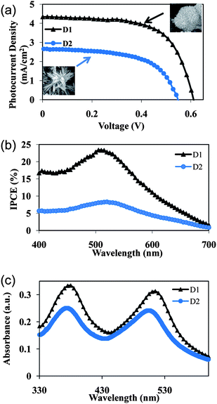 |
| | Fig. 10 (a) J–V characteristics, (b) IPCE curves of the DSSC and (c) UV-vis absorption spectra of dye loaded samples made with 0.04 and 1mM FeCl3 concentrations. | |
Table 2 Amount of dye absorbed and photovoltaic characteristics of 0.04 and 1 mM samples
| DSSC |
V
oc (V) |
J
sc (mA cm−2) |
FF (%) |
R at Voc |
R at Isc |
η (%) |
Dye adsorbed (moles/cm3) |
D (cm2s−1) |
| D1 |
0.6 |
4.3 |
63.5 |
77.7 |
8697.2 |
1.8 |
4.7 × 10⁻⁷ |
1.0 × 10⁻² |
| D2 |
0.5 |
2.7 |
58.5 |
119.6 |
8521.3 |
0.8 |
3.0 × 10⁻⁷ |
2.0 × 10⁻³ |
The photocurrent action spectra of the cells are shown in Fig. 10b, which displays IPCE spectra as a function of wavelength. The D1 cell shows a better photoelectrical response, and its absolute IPCE is obviously higher than that of the D2 cell over the entire wavelength region of 400–700 nm. This is also in good agreement with the observed higher Jsc of the D1 cell. The maxima of IPCE contributed by the N719 dye absorption at approximately 520 nm in the visible range are 23% for D1 and 8.4% for D2 respectively.
An ideal photoanode has to satisfy many criteria. These criteria can be illustrated by the continuity equation, introduced for the DSSC by Lindquist.54 The equation describes the electron generation, diffusion and interception.
| |  | (7) |
with boundary conditions,
| |  | (8) |
| |  | (9) |
where
n,
ηinj,
I0 and
α represent electron concentration, charge injection efficiency, incident
photon flux and absorption coefficient respectively. It is clear that the absorption coefficient is directly proportional to the effective molar concentration of the
dye, which is determined by the effective surface area available. Furthermore, the pore volume affects the DSSC performance by changing both the light absorption coefficient and the diffusion coefficient (
D). It is evident that increased
Jsc for the D1 cell comes from the high
dye loading capability of the film due to its high surface area. The influence of the surface area can also be observed from the relation of
Voc and
Jsc for a DSSC.
| |  | (10) |
where
Here Iinj is the current due to the electron from the excited dye, Ir the recombination current, ncb the concentration of electrons at the electrode interface and ket the rate constant for the reduction of the triiodide in the electrolyte by the electrons in the conduction band of Fe2O3. Because Iinj is proportional to the amount of dye on the electrode, it must increase on using a high surface area film. This is exactly what is observed for the cells made. The hybrid quasi-3D α-Fe2O3 nanostructures of D1 are superior to 1D nanorods of D2, as they have a high surface area and high pore volume. An increased Voc also suggests a decreased rate of Ir by lowering the electric resistance for the electron transport. In order to confirm this theory, UV-vis adsorption spectra of dye washed samples are recorded (Fig. 10c). The amount of dye loaded in the photoanode is obtained by desorbing the samples into 0.02 M NaOH (Table 2). Distinct peaks can be seen at ∼375 and 515 nm for D1 and D2, which are attributed to the metal-to-ligand charge transfer (MLCT) absorption band of the N719 dye. The results clearly show a higher dye absorbance for the D1 sample. This may be attributed to the presence of larger pores and high surface area of the film, leading to better dye wetting and loading.
It is already shown that the hybrid quasi-3D nanostructures are similar to 3D nanostructures but are superior to 1D nanorods as far as the surface area is concerned. To understand the role of morphology on the device performance and evaluate the diffusion coefficient, electrochemical impedance spectroscopy is carried out on the photoanode of D1 and D2. The complex impedance analysis helps in determining the interparticle interactions like grain boundary effects. Due to the polycrystalline nature of hybrid α-Fe2O3 samples, the barrier is modeled as double layer. It can be observed that Z′ decreases with the increase in frequency, indicating an increase in AC conductivity of the films. All the curves merge at high frequencies (>103 Hz) (Fig. 11a). The variation of Z′′ with frequency reveals peaks in the low-frequency region. The peak intensity for the 0.04 mM sample is lower and the peak position shifts towards a lower frequency. This indicates that the losses are lower in the film. The curves show that Z′′ exhibits a maximum value and then decreases continuously with a further increase in frequency. Such behavior indicates the presence of relaxation in the system (Fig. 11b). The Nyquist plots of D1 and D2 are shown in Fig. 11c. Both the samples show one arc, indicating that the relaxation time of the bulk and grain boundaries are close to each other and overlap. This response is attributed to FeIII/FeII redox species in the α-Fe2O3 matrix.55 Diameter of the D1 sample is smaller, indicating a smaller transport resistance. The intercept of the semicircle with the real axis at low frequency represents the sum of the resistances of the grains and grain boundaries. It is evident from the graph that resistance is lower for the D1 sample with a hybrid morphology, thus paving the way for better electrical transport.
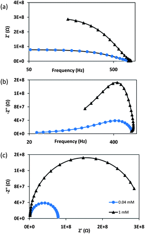 |
| | Fig. 11 Variation of (a) Z′, (b) Z′′ as a function of frequency and (c) Nyqusit plots of the doctor bladed films with 0.04 and 1 mM FeCl3 concentrations. | |
The electron transport in DSSCs is through diffusion since there is negligible band bending at the nanostructured semiconductor surface and the cationic species. The electrolyte solution surrounds the nanostructured electrode and screens the injected electrons effectively. In order for the injected electrons to reach the FTO, the electron diffusion length (L) should be longer than the thickness of the film. It is important to study the electron diffusion coefficient, since L = (Dτ)1/2, where τ is the electron lifetime also because D depends on the electrode morphology. The value of D is computed for both D1 and D2 samples for a 10 μm thick film (Table 2). Diffusion coefficient of hybrid quasi-3D nanostructures is higher than 1D nanorods. The effect of increased D can be many folds. The following relation relates D to the mobility of electrons (μe):
| |  | (12) |
As the diffusion coefficient increases, the mobility of the semiconductor increases. However, in a DSSC the mobility is trap controlled. This indicates that for the D1 sample of hybrid nanostructures the mobility is high and traps are smaller in number. Charge transport in metal oxides is expected to be governed by a multiple-trapping process, where the electrons thermally detrap from sub-bandgap states to the conduction band, and are transported a short distance before being retrapped.56 However, the location of the traps and trap densities are still debatable. The diffusion coefficient is inversely proportional to the number of traps.57 Assuming that the traps are located at the surface of the nanostructures, the diffusion coefficient should scale with r2/3, where r is the radius of nanoparticles.
With all other parameters equal, and assuming that electron motion is a random walk between uniformly distributed trap sites, idealized 1D diffusion should be faster than a fully 3D case.58 However, hybrid quasi-3D nanoflowers synthesized in this work lie in between 1D and 3D nanostructures. With identical structural sizes and fabrication method, it is reasonable to expect comparable trap densities in both 1D nanorods and quasi-3D nanoflowers. However, the transport performance of the nanorods is lower than quasi-3D nanoflowers. This could be due to the random orientation of the nanorods, some contacts exist between them. The other explanation could be that hybrid quasi-3D nanoflowers have more grain boundaries than 1D nanorods. Thus the number of possible necks is enhanced providing multiple paths for electrons to transverse. Kopidakis et al.59 has demonstrated a strong dependence of electron diffusion with crystal size and the nanoflowers used here are much larger than nanoparticles used for fabricating a standard DSSC. Therefore, quantitative comparison between the 3D nanoparticles and quasi-3D nanoflowers is not justified.
This work demonstrates a beginning stage for Fe2O3 as the potential candidate for photovoltaics. As already discussed, the synthesized α-Fe2O3 is an indirect band gap semiconductor. We feel any step taken for synthesizing direct band gap morphology would lead towards a more favorable material for the solar cell applications. This can be achieved by incorporating the structures with relevant dopants. It is also theoretically possible to enhance the conversion efficiency by changing the shape, size, porosity and thickness of the synthesized morphology. Detailed experimental investigations of these factors are under way in our laboratory.
Conclusions
In summary, quasi-3D nanoflowers of α-Fe2O3 are synthesized by a solution process using FeCl3 and Na2SO4 as the precursors. Tunability of the material is demonstrated through the change in precursor concentration. Formation of such structures requires a suitable Fe3+:SO42− ion ratio in the reaction mixture. The proposed growth mechanism indicates that an intermediate product of flower like goethite is formed first, which changes to the hematite phase on calcination at 400 °C. An in-depth understanding is gained as to how the surface area and transport properties are affected by variation in morphology. A unique 3D architecture with a relatively high surface area provides active sites for interaction of hydrogen gas resulting in excellent gas sensing behavior at room temperature (7.1 at 50 ppm). The high surface area also leads to better dye wetting in the DSSC, which contributes to a 1.8% power conversion efficiency. A systematic understanding of the devices’ performance is derived from the investigation of few important parameters, which include surface area, grain boundaries and diffusion coefficients of the photoanode film. The understanding of structurally (morphology) directed properties will have a huge impact on the future utilization of such hybrid nanostructures for myriad surface dominated applications such as photocatalysts, solar cells, sensors, etc.
Acknowledgements
This work is supported by the National University of Singapore (NUS) grant R-263-000-532-112 and R-263-000-508-720.
References
- W. S. Chae, S. W. Lee and Y. R. Kim, Chem. Mater., 2005, 17, 3072 CrossRef CAS.
- S. Agarwala, M. Kevin, A. S. W. Wong, C. K. N. Peh, V. Thavasi and G. W. Ho, ACS Appl. Mater. Interfaces, 2010, 2, 1844 CAS.
- Q. F. Zhang, T. P. Chou, B. Russo, S. A. Jenekhe and G. Z. Cao, Adv. Funct. Mater., 2008, 18, 1654 CrossRef CAS.
- H. X. Yang, J. F. Qian, Z. X. Chen, X. P. Ai and Y. L. Cao, J. Phys. Chem. C, 2007, 111, 14067 CAS.
- A. Narayanaswamy, H. F. Xu, N. Pradhan, M. Kim and X. Peng, J. Am. Chem. Soc., 2006, 128, 10310 CrossRef CAS.
- C. Q. Hu, Z. H. Gao and X. R. Yang, Chem. Lett., 2006, 35, 1288 CrossRef CAS.
- M. Hermanek, R. Zboril, I. Medrik, J. Pechousek and C. Gregor, J. Am. Chem. Soc., 2007, 129, 10929 CrossRef CAS.
- L. H. Huo, W. Li, L. H. Lu, H. N. Cui, S. Q. Xi, J. Wang, B. Zhang, Y. C. Shen and Z. H. Lu, Chem. Mater., 2000, 12, 790 CrossRef CAS.
- Z. C. Wu, K. Yu, S. D. Zhang and Y. Xie, J. Phys. Chem. C, 2008, 112, 11307 CAS.
- S. W. Cao and Y. J. Zhu, J. Phys. Chem. C, 2008, 112, 6253 CAS.
- L. Li, Y. Chu, Y. Liu and L. Dong, J. Phys. Chem. C, 2007, 111, 2123 CAS.
- X. Wen, S. Wang, Y. Ding, Z. Lin Wang and S. Yang, J. Phys. Chem. B, 2005, 109, 215 CrossRef CAS.
- K. Woo, H. J. Lee, J. P. Ahn and Y. S. Park, Adv. Funct. Mater., 2003, 15, 1761 CAS.
- C. J. Jia, L. D. Sun, Z. G. Yan, L. P. You, F. Luo, X. D. Han, Y. C. Pang, Z. Zhang and C. H. Yan, Angew. Chem., Int. Ed., 2005, 44, 4328 CrossRef CAS.
- S. H. Zhan, D. R. Chen, X. L. Jian and S. S. Liu, J. Colloid Interface Sci., 2007, 308, 265 CrossRef CAS.
- N. O. Jones, B. V. Reddy, F. Rasouli and S. N. Khanna, Phys. Rev. B: Condens. Matter Mater. Phys., 2005, 72, 1 CrossRef.
- S. Hamada and E. Matijević, J. Colloid Interface Sci., 1981, 84, 274 CrossRef CAS.
- L. Ferretto and A. Glisenti, J. Mol. Catal. A: Chem., 2002, 187, 119 CrossRef CAS.
- Y. Liu and D. Sun, J. Hazard. Mater., 2007, 143, 448 CrossRef CAS.
- H. Fu, X. Quan and H. Zhao, J. Photochem. Photobiol., A, 2005, 173, 143 CrossRef CAS.
- I. Ceasar, A. Kay, J. A. G. Martinez and M. Grätzel, J. Am. Chem. Soc., 2006, 128, 4582 CrossRef.
- G. Jain, M. Balasubramanian and J. J. Xu, Chem. Mater., 2006, 18, 423 CrossRef CAS.
- G. Goodlet, S. Faty, S. Cardoso, P. P. Freitas, A. M. Simoes, M. G. Ferreira and M. D. Belo, Corros. Sci., 2004, 46, 1479 CrossRef CAS.
- N. Özer and F. Tepehan, Sol. Energy Mater. Sol. Cells, 1999, 56, 141 CrossRef.
- J. A. Glasscock, P. R. F. Barnes, I. C. Plum, A. Bendavid and P. J. Martin, Thin Solid Films, 2008, 516, 1716 CrossRef CAS.
- J. G. Yu, X. X. Yu, B. B. Huang, X. Y. Zhang and Y. Dai, Cryst. Growth Des., 2009, 9, 1474 CAS.
- G. Eranna, B. C. Joshi, D. P. Runthala and R. P. Gupta, Crit. Rev. Solid State Mat. Sci., 2004, 29, 111 CrossRef CAS.
- G. Neri, A. Bonavita, S. Galvagno, P. Siciliano and S. Capone, Sens. Actuators, B, 2002, 82, 40 CrossRef.
- O. K. Tan, W. Cao and W. Zhu, Sens. Actuators, B, 2000, 63, 129 CrossRef.
- G. Wang, X. Gou, J. Horvat and J. Park, J. Phys. Chem. C, 2008, 112, 15220 CAS.
- F. He, J. Han, Y. Zheng, H. Yu and Y. Wang, Jpn. J. Appl. Phys., 1994, 33, 2626 CrossRef CAS.
- D. Mao, J. Yao, X. Lai, M. Yang, J. Du and D. Wang, Small, 2011, 7, 578 CrossRef CAS.
- Q. Hao, S. Liu, X. Yin, Z. Du, M. Zhang, L. Li, Y. Wang, T. Wang and Q. Li, CrystEngComm, 2011, 13, 806 RSC.
- F. Zhang, H. Yang, X. Xie, L. Li, L. Zhang, J. Yu, H. Zhao and B. Liu, Sens. Actuators, B, 2009, 141, 381 CrossRef.
- J. Chen, L. Xu, W. Li and X. Gou, Adv. Mater., 2005, 17, 582 CrossRef CAS.
- F. Gao, Y. Wang, D. Shi, J. Zhang, M. Wang, X. Jing, R. Humphry-Baker, P. Wang, S. M. Zakeeruddin and M. Graetzel, J. Am. Chem. Soc., 2008, 130, 10720 CrossRef CAS.
- B. C. O'Regan, K. Bakker, J. Kroeze, H. Smit, P. Sommeling and J. R. Durrant, J. Phys. Chem. B, 2006, 110, 17155 CrossRef CAS.
- M. Law, L. E. Greene, J. C. Johnson, R. Saykally and P. D. Yang, Nat. Mater., 2005, 4, 455 CrossRef CAS.
- J. R. Jennings, A. Ghicov, L. M. Peter, P. Schmuki and A. B. Walker, J. Am. Chem. Soc., 2008, 130, 13364 CrossRef CAS.
- Y. Suzuki, S. Ngamsinlapasthian, R. Yoshida and S. Yoshikawa, Cent. Eur. J. Chem., 2006, 4, 476 CrossRef CAS.
- S. Pavasupree, S. Ngamsinlapasthian, M. Nakajima, Y. Suzuki and S. Yoshikawa, J. Photochem. Photobiol., A, 2006, 184, 163 CrossRef CAS.
- C. H. Ku and J. J. Wu, Appl. Phys. Lett., 2007, 91, 093117 CrossRef.
- D. Du and M. Cao, J. Phys. Chem. C, 2008, 112, 10754 CAS.
- S. Zeng, K. Tang, T. Li, Z. Liang, D. Wang, Y. Wang, Y. Qi and W. Zhou, J. Phys. Chem. C, 2008, 112, 4836 CAS.
-
B. D. Cullity. Elements
of X-Ray Diffraction, Second Ed., Addison-Wesley Pub. Co., Massachusetts, 1978 Search PubMed.
- L. A. Marusak, R. Messier and W. B. White, J. Phys. Chem. Solids, 1980, 41, 981 CrossRef CAS.
- N. C. Debnath and A. B. Anderson, J. Electrochem. Soc., 1982, 129, 2169 CrossRef CAS.
- L. P. Zhu, H. M. Xiao, X. M. Liu and S. Y. Fu, J. Mater. Chem., 2006, 16, 1794 RSC.
- Z. Z. Sun, X. M. Feng and W. H. Hou, Nanotechnology, 2007, 18, 455607 CrossRef.
- S. Zeng, K. Tang, T. Li and Z. Liang, J. Phys. Chem. C, 2010, 114, 274 CAS.
- S. Kambe, K. Murakoshi, T. Kitamura, Y. Wada, S. Yanagida, H. Kominami and Y. Kera, Sol. Energy Mater. Sol. Cells, 2000, 61, 427 CrossRef CAS.
- G. Wang, X. Gou, J. Horvat and J. Park, J. Phys. Chem. C, 2008, 112, 15220 CAS.
- J. Chen, L. Xu, W. Li and X. Gou, Adv. Mater., 2005, 17, 582 CrossRef CAS.
- S. Sodergren, A. Hagfeldt, J. Olsson and S. E. Lindquist, J. Phys. Chem., 1994, 98, 5552 CrossRef.
- S. S. Shinde, A. V. Moholkar, J. H. Kim and K. Y. Rajpure, Surf. Coat. Technol., 2011, 205, 3567 CrossRef CAS.
- A. J. Frank, N. Kopidakis and J. van de Lagemaat, Coord. Chem. Rev., 2004, 248, 1165 CrossRef CAS.
- S. Nakade, Y. Saito, W. Kubo, T. Kitamara, Y. Wada and S. Yanagida, J. Phys. Chem. B, 2003, 107, 8607 CrossRef CAS.
- K. Zhu, N. R. Neale, A. Miedaner and A. J. Frank, Nano Lett., 2007, 7, 69 CrossRef CAS.
- N. Kopidakis, N. R. Neale, K. Zhu., J. van de Lagemaat and A. J. Frank, Appl. Phys. Lett., 2005, 87, 202106 CrossRef.
Footnote |
| † Electronic supplementary information (ESI) available. See DOI: 10.1039/c1nr10856e |
|
| This journal is © The Royal Society of Chemistry 2012 |
Click here to see how this site uses Cookies. View our privacy policy here.