Flexible planar microfluidic chip employing a light emitting diode and a PIN-photodiode for portable flow cytometers†
Siegfried W.
Kettlitz
*,
Sebastian
Valouch
,
Wiebke
Sittel
and
Uli
Lemmer
Light Technology Institute, Karlsruhe Institute of Technology, Kaiserstr. 12 Geb. 30.34, Karlsruhe, Baden-Württemberg 76131, Germany. E-mail: siegfried.kettlitz@kit.edu
First published on 15th November 2011
Abstract
Detection of fluorescence particles is a key method of flow cytometry. We evaluate the performance of a design for a microfluidic fluorescence particle detection device. Due to the planar design with low layer thicknesses, we avoid optical components such as lenses or dichroic mirrors and substitute them with a shadow mask and colored film filters. A commercially available LED is used as the light source and a PIN-photodiode as detector. This design approach reduces component cost and power consumption and enables supplying the device with power from a standard USB port. From evaluation of this design, we obtain a maximum particle detection frequency of up to 600 particles per second at a sensitivity of better than 4.7 × 10⁵ MESF (molecules of equivalent soluble fluorochrome) measured with particles for FITC sensitivity calibration. Lowering the flow rate increases the instrument sensitivity by an order of magnitude enabling the detection of particles with 4.5 × 10⁴ MESF.
1 Introduction
The use of microfluidic Lab-on-a-Chip systems in flow cytometric applications has gained momentum in recent years.1–4 Especially in conjunction with printable microfluidics5,6 and organic electronics,7–9 research towards the creation of low-cost printable Lab-on-a-Chip systems for a wide range of applications is attractive. Within this paper we present a thin flexible planar microfluidic chip optimized for fluorescence particle detection using a commercially available light-emitting diode (LED) as light source and a low-cost photodiode as detector without voluminous or expensive optical components such as imaging lenses or dichroic optical filters.The applicability of an LED as an excitation source in a flow cytometric system10–12 has been shown over a decade ago.12 With the Agilent 2100 Bioanalyzer, which also utilizes a blue LED for excitation, a commercial product is on the market. These systems, however, still use discrete optics such as lenses and dichroic mirrors which should be avoided to simplify the design and enable miniaturization. Other systems use laser diodes, which are much cheaper than gas lasers.13–19 These systems, however, require additional spatially aligned optical components to focus the laser on the microchannel. The detection of fluorescence particles is related to the detection of fluorescent dye concentrations18,20–26 in which steady state signals are detected instead of transient signal pulses generated by passing particles.
Expensive and sensitive components such as photo multiplier tubes (PMT) are replaced with solid state avalanche photodiodes (APD) or even PIN photodiodes.16,18,20,26 When using photo multiplier tubes or avalanche photodiodes, only low light intensities can be used requiring high quality optical filters to separate the fluorescence from the excitation light. PIN photodiodes do not have this limitation and are much cheaper. This is particularly true for the case of cytometers, where cell counting rather than the determination of a concentration is performed. In such applications, the residual light signal offset can be subtracted from the transient fluorescence signal. In consequence, the design can tolerate more light on the detector from the excitation source or other sources without distorting the measured signal.
Here, we therefore use a novel approach to maximize the optical yield of fluorescence emission by placing the excitation light source and the fluorescence detector very close to the microfluidic channel. This allows to remove all beam forming components from the LED excitation channel and place the light emitting chip directly on the substrate. Our detection system is designed to use only low power components and it is fully powered by the 5 V, 500 mA provided by an ordinary USB-port making it very portable and versatile in its application.
While classical flow cytometers usually achieve sensitivities much better than 103 MESF for a wide range of fluorophores, replacing expensive components and moving to microfluidic systems has an impact on sensitivity of the devices. The Agilent 2100 Bioanalyzer has a sensitivity of 2 × 10⁶ MESF FITC when using the blue LED for excitation which limits the range of applications.27 The low sensitivity does not solely root in the use of an LED as the excitation source itself12 or the use of microfluidics since sensitivities of <600 MESF FITC have been reported for other microfluidic systems using solid state lasers.1
In this manuscript we report a simple design for a microfluidic particle detector based on an LED and a simple PIN-photodiode. The emphasis of our approach is on simplicity of design using low-cost components while still maintaining a detection performance sufficient for a wide range of applications. Sensitivities of much less than 103 MESF are not required when dealing with brightly stained cells having intensities in the 105 MESF FITC range.28–31
2 Materials and methods
The particle detection system consisting of electronic and optical components is schematically shown in Fig. 1. For the detection of moving fluorescent particles flowing through the microfluidic channel, we need excitation light which is supplied by an LED and filtered by an excitation filter. The emission filter transmits fluorescence light and blocks excitation light. The mask foil restricts the effective area of the photodiode. This reduces the amount of excitation light which is not blocked by the emission filter leading to an increased sensitivity of the instrument. The mask foil also shortens the pulses obtained from moving particles which increases the maximum particle throughput. An important feature of the instrument is the preamplifier which consists of a differential amplifier stage which minimizes noise from electrical interference and a high pass filter which removes the DC-offset caused by the residual excitation light. In the following we describe the optical and electrical features of the device in more detail. After that, we discuss the microfluidic structure used for particle focusing.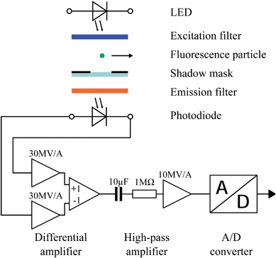 | ||
| Fig. 1 Schematic diagram of the detection system. An LED supplies the excitation light, which is filtered with the excitation filter. The passing fluorescence particle absorbs the excitation light and emits light of longer wavelength. The shadow mask restricts the detection area. The emission filter absorbs excitation light and transmits fluorescence light to the photodiode. At the differential amplifier, the current signal of the photodiode is amplified by 60 MV A−1. A high pass amplifier removes the DC-offset from the signal. After that it is digitized by the A/D-converter. | ||
2.1 Optical
The most important feature of our microfluidic device is the low thickness of the different functional layers of our optofluidic system. The cross section at the detection zone is shown in Fig. 2. The LED has to be placed on top of layer D which is the excitation filter to block the low energy wing of the LED emission. The polydimethylsiloxane (PDMS) layers Ca and Cb enclose the microfluidic channel at F. The fluorescence light generated within the channel can then be detected through layer B which is the mask foil spatially defining the detection area. An additional emission filter (not shown in Fig. 2) can be placed between the mask foil and the PIN photodiode.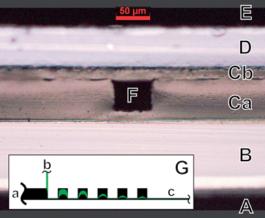 | ||
| Fig. 2 Cross-section of the bonded microfluidic chip. A: Detection side. B: The mask foil with the mask side facing the PDMS. C: PDMS layers a: with microstructures and b: capping layer. D: Excitation filter. E: Illumination side. F: Microchannel completely encapsulated in PDMS. The light emitting substrate of the LED will be placed directly on the excitation filter to minimize the distance to the microchannel. An emission filter is placed between the mask foil and the photo detector. G: Inset showing the focusing structure with a: sheath flow inlet, b: sample flow inlet and c: measurement region. The sheath fluid is shown in black and the sample fluid containing the fluorescent particles is shown in green. The focusing of the particles is drawn according to Lee et al.32 | ||
We have minimized the thicknesses of layers D and Cb between the channel and the LED to maximize the excitation light intensity in the channel. We removed the optical capping from the LED and placed the LED directly on the excitation filter (Fig. 2-D). The excitation filter itself is an absorption based color filter (Lee Filters, filter no. 071HT). We use the high temperature version of this filter for two reasons. Firstly, the LED produces very high intensity light leading potentially to filter degradation and deformation even at diode currents much lower than the maximum design current. Secondly, the high temperature version of this filter is thinner with a thickness of about 56 μm compared to 110 μm for the standard version. This allows positioning of the LED chip very close to the microfluidic channel. In order to avoid total reflection losses between the LED and the excitation filter, liquid PDMS (Dow Corning, Sylgard 184 silicone elastomer kit) without curing agent is used. Optionally, the addition of a curing agent would glue the LED to the microfluidic chip. A thin layer of PDMS of 10 μm to 20 μm thickness between the microfluidic channel and the excitation filter is used for bonding and protection of the filter.
On the detection side, we align a mask foil to the microfluidic channel with the mask side facing towards the channel structure. The measurement region of the mask foil is black except for a transmission window with 200 μm width and various lengths. The size of the width is a compromise of alignment precision and the minimization of residual background light from the LED impinging on the photodiode. Using windows of different lengths allows the study of its influence on the height and the shape of the signal pulses generated by passing particles. By minimizing the thickness of layer Ca between the microfluidic channel and the transmission window, we maximize the solid angle, which can be collected from the particle emission. Between the mask foil and the photodiode, an emission filter (2 sheets of Lee Filters, no. 767) is used to suppress the excitation light. An additional IR filter is placed in front of the PIN-photodiode in order to filter out residual IR light emitted from the LED. Microoptics such as integrated lenses or mirrors cannot improve the excitation intensity or detection efficiency significantly because our design already exhibits a large solid angle due to the short distances to the light source and photodiode. Exceptions are mirroring filters which allow additional backside illumination and collection of backside fluorescence which both could theoretically double the detected fluorescence intensity. Flexible dichroic mirrors33 with low angular dependence could be used for this purpose.
The transmission spectra of the optical filters are shown in Fig. 3. The combination of one blue excitation filter with two yellow emission filters results in a good suppression of the light transmission up to 650 nm wavelength. The transmittance at 500 nm is below 1 × 10⁻³ which is important since this is close to the emission peak of the excitation light source.
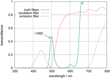 | ||
| Fig. 3 Transmittance spectra of the optical filters used for excitation (Lee Filters, no. 071HT, dotted line) and emission (2 sheets of Lee Filters no. 767, dashed line) and both filters combined (solid line, amplitude enlarged by a factor of 1000). Combining both filters eliminates most light below 650 nm wavelength with some residual transmittance around 500 nm. The transmittance above 650 nm is reduced by an additional IR-Filter in front of the photodiode. | ||
Since the size of the light emitting diode of 1 mm × 1 mm is significantly larger than the distance of about 100 μm to the excited fluorescence particle the incident light has a large solid angle. This hinders the applicability of crossed polarizers for further reduction of transmitted excitation light20 in this system, due to the large solid angle and short distance to the light source. The advantage of this geometry, however, is the maximized light intensity at the fluorescence excitation area.
2.2 Electrical
The electrical components consist of the LED (Luxeon, Rebel LXML-PR01-0425) as excitation light source, the photodiode (Osram, BPW 34), a preamplifier, a USB sound-card with a CM108-chip from C-Media as A/D converter with the input connected to the preamplifier and voltage regulators.In order to supply the needed voltages and currents to the transimpedance amplifier circuit and LED light source with low noise, we use a switching DC–DC converter to convert the 5 V delivered by the USB port to ±15 V and use a linear regulator to supply +10 V for the LED. Using a variable resistor, a current of 50 mA is adjusted. In addition, two linear voltage regulators supply ±12 V for the transimpedance amplifier. The total maximum draw at the current supply is 430 mA of which the USB hub alone draws 80 mA, plugging in the sound card adds 50 mA. Adding the preamplifier with the voltage converters leads to an increase of 130 mA. Switching on the LED adds another 170 mA current draw. Since the LED uses only 50 mA at a typical voltage of 3.15 V, a dedicated current source could be used to drive the LED directly from the 5 V supply without first converting it to 15 V. This would allow much higher LED currents of over 200 mA without an additional power supply. We limit the LED current to 50 mA as a compromise between the degradation speed of the excitation filter and the instrument's sensitivity. Using a different filter dye with less absorption and decreased degradation would enable the use of higher LED intensities.
We use a dual transimpedance amplifier stage with a subsequent difference amplifier shown in Fig. 1 in order to minimize electromagnetic interference. A high amplification of 30 MV A−1 at both transimpedance amplifier stages is used. An RC high pass filter with a time constant of 10 s between the last preamplifier stage and the A/D-converter provides DC-decoupling. The very low edge frequency enables measurement of the transient signals generated by slow flowing particles. We minimize the amount of components for the analog signal processing part with the use of a single low cost TL074 chip providing 4 low noise operational amplifiers.
The on-board high pass capacitor of the sound card is bypassed for low frequency measurements of transients generated by slow moving particles. For recording of the digitized signals, a simple audio recording program is used.
Our amplifier design requires a low noise light source since it only compensates for electrical interference. Optical noise could be compensated for by using a separate monitor diode and subtracting both signals. This concept has been demonstrated for extinction measurements using noisy laser light sources by Steinkamp et al.34 Since our employed light source is low noise, we chose the simpler design without monitor diode. For further developments using organic light emitting diodes which may emit light with higher fluctuations35–37 the incorporation of a monitoring diode could improve the signal quality significantly.
2.3 Particle focusing
In order to make high quality measurements, the focusing of particles into a narrow stream in the middle of the flow channel is necessary when using focused excitation light sources. When illuminating with a focused laser with a spot size of a few tens of microns, the particles have to be focused to a much narrower zone than required with our comparably large LED. Another benefit, however, from focusing is that the particles all move in the center of the laminar flow and therefore exhibit a low variance of velocities. This is desirable since all particles produce the same pulse shapes with different amplitudes which makes the measurement of particle intensities easier. Utilizing the homogenous illumination of the LED we show the detection of well focused particles at high speed and also the detection of non-focused particles at a much lower speed.Literature describes a multitude of different methods and structures for microfluidic particle focusing. The use of bent structures38–40 would require high resolution lithography which would conflict with our low-cost lithography approach. Multilayer structures41–43 are incompatible with our single layer lithography process. Sheathless focusing structures40,44–47 are viable candidates for our design. Especially sheathless inertial focusing of particles into a single stream40 is interesting to avoid position dependent measurement variations. However, in order to have the flexibility of changing the particle rate and velocity independently, we chose a design using a single sheath flow relying on Dean flow for focusing presented by Lee et al.32 Its advantages are simplicity in implementation due to the rectangular structures and the possibility to adjust the particle rate and velocity independently by changing the pumping rates of sample and sheath flow.
The employed particle focusing structure consists of five consecutive constriction zones in the 50 μm high and 350 μm wide channel shown in the inset in Fig. 2-G. The constriction structures are 300 μm by 300 μm wide and spaced by 300 μm. The sixth constriction zone is formed by the 50 μm wide flow channel which is extended throughout the measurement region. The particles should be focused in the middle of the flow channel after the focusing structure in Fig. 2-Gc. For further information about the performance of the focusing structure we refer to Lee et al.32
3 Device fabrication
We use a well known soft lithography method to produce microfluidic PDMS chips.48A 50 μm thick layer of photoresist (Microchem, SU8-2050) is spin coated on a silicon wafer. Using a mask aligner (MJB3 Standard, Suss), we expose the photoresist with the desired structure through an offset film (BuWeMedia, offset film 3600 dpi). Upon subsequent development, the negative of the microfluidic channel structure remains on the wafer.
We use PDMS (Dow Corning, Sylgard 184 silicone elastomer kit) to form a negative replica of the SU8-master. The standard mixing ratio of 1![[thin space (1/6-em)]](https://www.rsc.org/images/entities/char_2009.gif) :10 curing agent to base material is used. The master is treated with HMDS (Sigma-Aldrich, hexamethyldisilazane) before pouring PDMS on the structures. The black mask foil (also BuWeMedia, offset film 3600 dpi) is treated with an oxygen plasma at 50 W (Diener electronic, model Femto) for 240 s. Then it is placed on the PDMS with the mask side facing down. Afterwards, the mask windows are aligned to the microfluidic channel under a microscope with the PDMS still in liquid phase. The transparent window in the black mask is then aligned onto the channel near the exit of the focusing structure. After alignment, the wafer is placed on a hotplate at 100 °C for 600 s to cure the PDMS. The mask foil is then removed from the master wafer and now acts as a substrate for the microfluidic system. Holes are punched through the foil at the reservoirs for fluid connections.
:10 curing agent to base material is used. The master is treated with HMDS (Sigma-Aldrich, hexamethyldisilazane) before pouring PDMS on the structures. The black mask foil (also BuWeMedia, offset film 3600 dpi) is treated with an oxygen plasma at 50 W (Diener electronic, model Femto) for 240 s. Then it is placed on the PDMS with the mask side facing down. Afterwards, the mask windows are aligned to the microfluidic channel under a microscope with the PDMS still in liquid phase. The transparent window in the black mask is then aligned onto the channel near the exit of the focusing structure. After alignment, the wafer is placed on a hotplate at 100 °C for 600 s to cure the PDMS. The mask foil is then removed from the master wafer and now acts as a substrate for the microfluidic system. Holes are punched through the foil at the reservoirs for fluid connections.
A slide of blue filter foil (Lee Filters, no. 071HT) is treated for 120 s with oxygen plasma at 50 W to improve the bonding to the PDMS. Subsequently PDMS is poured onto the blue foil. A thin layer with a thickness between 10 μm and 20 μm is obtained by spin-coating at 1500 RPM for 60 s followed by 4000 RPM for 60 s. Subsequently, the mask foil is pre-cured for 60 s at 100 °C.
Before bonding both layers, the substrate with the channels is treated using an oxygen plasma at 50 W for 30 s. Both pieces are pressed together and left to cure at room temperature for at least 12 h.
4 Measurement setup
The microfluidic chip is connected via flexible tubes to two syringes and a waste container. The two syringes are driven by two syringe pumps (Landgraf Laborsysteme, model LA-30). The pumping rate for the sample flow is 50 μl h−1 for all measurements. For the pumping rate of the sheath flow, we use two rates. In the following, 3000 μl h−1 is referred to as the high flow rate and 150 μl h−1 is referred to as the low flow rate. The sheath flow and sample flow consist of 10 times concentrated PBST (Sigma-Aldrich, phosphate buffered saline with Tween-20 10× concentrate) solution diluted 2:1 with deionized water. We use this mixing ratio since higher dilutions of the concentrated PBST have a lower specific density which leads to a fast sinking of the polystyrene particles during the measurements. Per 1 ml of sample fluid 100 μl of dispersed calibration particles (Kisker Biotech, Yellow Calibration Particles, 6.2 μm) are added. The calibration fluid contains particle types with different intensities. In our measurements, we detect the brightest particles with a calibrated intensity of 4.9 × 10⁶, 4.7 × 10⁵, 4.5 × 10⁴ MESF FITC (molecules of equivalent soluble fluorophores of FITC equivalent). Although the actual fluorophore of these particles is unspecified by the manufacturer, they are specifically designed for FITC calibration.
5 Results
5.1 Particle focusing
Using a high flow rate of 3000 μl h−1 for the sheath flow and 50 μl h−1 for the sample flow, we measure a coefficient of variance (CV) for the particle velocities of 3.1% directly after the focusing structure. The histogram of particle velocities is shown in Fig. 4. The shape of the histogram with most particles at the highest velocity and some particles with slightly lower velocities conforms with the assumption of a focusing of the majority of particles in the center of the channel where the highest velocity is present with a lower particle density towards the walls. This shows that the employed particle focusing method is functional.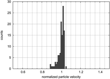 | ||
| Fig. 4 Histogram of the particle velocities after the focusing structure. | ||
At measurement points further away from the focusing structure, we obtain higher CV values of about 0.1 over a large variation of flow rates, which is a sign of other hydrodynamic forces46,47,49 acting on the 6.2 μm sized particles.
5.2 Signal pulse forms
Since only one fluorescent particle should be in the measurement area at a time in order to avoid interference, we investigate the use of different mask window lengths of 18 μm, 49 μm, 96 μm, 211 μm, 436 μm, 888 μm, and 1779 μm. A shorter window will allow a higher particle density in the analyte while a longer window results in a longer exposure time which reduces the measurement noise after low pass filtering of the signal.Kiesel et al.19 presented a laser based design which also uses a long detection window formed by a shadow mask. In their design, the window contains a patterned shadow mask. A large area avalanche photodiode is used to detect the spatially modulated signal. This modulation is used to improve the spatial resolution well below the window dimensions. Adding the same modulation pattern to the mask window would also be possible in our system.
In order to obtain the signal profile from passing fluorescence particles for different window lengths, we measure the intensity profiles for a low flow rate and afterwards for the high flow rate. The results are shown in Fig. 5.
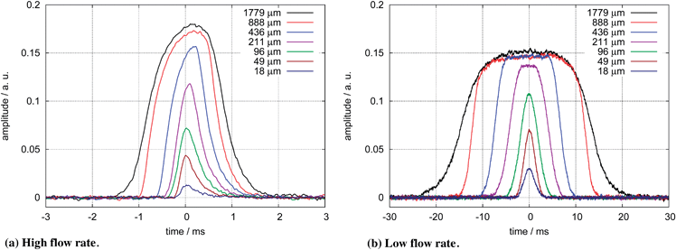 | ||
| Fig. 5 Typical pulse shapes measured for different window lengths for the high flow rate in subfigure a and the low flow rate in subfigure b. Shown is the unfiltered fluorescence signal of particles with an intensity of 4.9 × 10⁶ MESF FITC digitized at a 48 kHz sampling rate. | ||
Since the LED emits light on a length of 1000 μm along the channel, the intensity profile will be shaped mainly by the LED for the longest mask window of 1779 μm. Window lengths much shorter than the LED size exhibit a uniform particle excitation over the whole length. This is confirmed by the pulse forms in Fig. 5b.
Another factor which shapes the pulse form is the preamplifier for the photodiode signal. The electrical response of the transimpedance amplifier to an optical rectangular signal applied to the photodiode results in a rise time of 0.5 ms. This plays a significant role in the measured pulse shapes for the high flow rate shown in Fig. 5a but only for very short window lengths for the low flow rate in Fig. 5b.
In order to obtain the particle intensity, different approaches have to be taken with these signals. For the high flow rate, the particle velocity shows little deviation therefore the integral of the signal pulse is proportional to the particle intensity. A suitable low pass filter minimizes the noise and the peaks of the filtered signal correlate with the particle intensities.
For the low flow rate, this approach is partially blocked by the large variance in particle velocities leading to a large variance in the pulse integrals. We cannot simply use an arbitrary low pass filter to obtain the particle intensity. Obtaining the particle intensity from the pulse peak would be possible but leads to a noisy result. We can use the flat top of the pulse shapes shown in Fig. 5b for window lengths of at least 211 μm. Filtering the flat top with a moving average filter with a filter length not longer than the shortest flat top leads to a filtered signal with decreased noise and signal peaks which are independent of the particle speed. Since the particles cannot move faster than the liquid in the center of the channel the filter length is given by this velocity.
The large homogenous illumination area of the LED works in favor of this detection method by creating signals with a flat top. Since slower particles are illuminated for a longer time, we expect higher instrument sensitivity in exchange for a lower maximum particle throughput.
The achievable particle throughput can be estimated from the width of the pulse shapes in Fig. 5. We use the full width half maximum to estimate the pulse width. For the low flow rate, we estimate a maximum detection rate of non-overlapping particles of 36 particles per second with the longest window and 406 particles per second with the shortest window. For the high flow rate we estimate maximum particle rates from 600 particles per second to 2526 particles per second.
5.3 Fluorescence intensity histograms
In Fig. 6, the particle intensity histograms corresponding to the pulse forms in Fig. 5 are shown.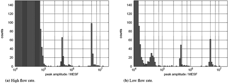 | ||
| Fig. 6 Histograms of detected particle amplitudes during 5 min of measurement. The high and low flow rates have a sheath flow rate of 3000 μl h−1 and 150 μl h−1, respectively. The sample flow rate is 50 μl h−1 in both cases. The high counts for low amplitudes are caused by false detections due to signal noise. They would be suppressed by a threshold in the detector. For the low flow rate, the noise floor is lower and a third particle population becomes visible. | ||
In order to reduce computational complexity, we reduce the sample rate of the recorded signals by a factor of 5 and 30 for the high and low flow rate, respectively. Subsequently a low-pass filter using a finite impulse response (FIR) filter convolution with a Hann window,50 which has a length of 10 samples, is used to suppress high frequency noise. A median filter with a window length of 1000 samples is used to extract the baseline of the signal which is then subtracted. After that, a moving average filter with a window length of 20 samples is used to obtain the signal peaks. The particles are then detected from local maxima in the signal and the amplitude is manually adjusted so that the highest intensity particle amplitude of the calibration particles matches 4.9 × 10⁶ MESF FITC. This adjustment eliminates a range of unknown linear factors in the signal path.
Using the high flow rate, we are able to clearly detect particles with 4.7 × 10⁵ MESF FITC intensity which is the initially referenced value for stained white blood cells.30 The histogram in Fig. 6a shows two clear peaks for the two detectable particle intensities.
For the low flow rate we are able to lower the noise floor by almost an order of magnitude. In Fig. 6b particles with an intensity of 4.5 × 10⁴ MESF FITC can be distinguished in the histogram. The amplitudes for these particles are much more spread in the histogram and lower than expected which may result from various effects. Low frequency sources such as 1/f noise of the amplifier, variations in the flow rate of the liquid and electromagnetic interference add to the variance of amplitudes detected. The additional extinction of residual excitation light from the passing particle lowers the detected amplitude. Better filtering of the excitation light will suppress this problem.
The expected intensity independent increase in variance of the detected amplitudes due to the lower particle focusing quality can not be seen when comparing the histograms for high intensity particles in Fig. 6a and Fig. 6b. This leads to the conclusion that particle focusing is not as important for accurate particle detection for LED excitation as it is with focused laser excitation.
6 Conclusion and outlook
In conclusion, we have demonstrated a low cost microfluidic device for flow cytometric applications. This device does not require optical beam forming components such as lenses or fibers. The LED illuminated area of 1 mm by 1 mm is, compared to the focused spot of a LASER, very large. This greatly reduces alignment requirements. The sensitivity determined by the noise floor is approximately 1 × 10⁵ MESF FITC at a high flow rate of 3000 μl h−1 which should be sufficient for the detection of a range of stained blood cellse.g. for antibodies of CD14,28CD20,29CD4529,30 and CD52.31A reduction of the flow rate extends the detection range to 4.5 × 10⁴ MESF FITC and further sensitivity improvements can be obtained by increasing the continuous LED current by a factor of 20 to the maximum design current. Using dichroic plastic filters, possibly in combination with absorbing or polarizing filters promises a further decrease of transmitted excitation light while increasing the efficiency of fluorescence detection. Modulating the excitation light source promises to reduce interference noise from electrical and optical sources, which reduces the shielding requirements during measurement and further reduces the costs of the microfluidic components.
We have shown the ability of our design to detect and classify fluorescent beads. Further investigations using stained blood cells need to confirm the viability of our approach for biological applications. The real-time operation capability of USB-audio chips with data processing in a personal computer is useful for the further development of applications such as cell sorting. Since mobile devices such as tablet computers are becoming increasingly available, the power supply over the USB port opens a wide range of mobile applications.
Acknowledgements
We acknowledge financial support by the DFG Center for Functional Nanostructures, project number A4.2.References
- D. Wlodkowic, J. Skommer and Z. Darzynkiewicz, Cytometry, Part A, 2010, 77A, 591–606 CrossRef CAS.
- J. Komen, F. Wolbers, H. Franke, H. Andersson, I. Vermes and A. van den Berg, Biomed. Microdevices, 2008, 10, 727–737 CrossRef CAS.
- D. Wlodkowic, K. Khoshmanesh, J. C. Sharpe, Z. Darzynkiewicz and J. M. Cooper, Anal. Chem., 2011, 83, 6439–6446 CAS.
- D. Wlodkowic and Z. Darzynkiewicz, Methods In Cell Biology, Vol 102: Recent Advances In Cytometry, Part A: Instrumentation, Methods, Fifth Edition, 2011, pp. 105–125 Search PubMed.
- H. Dong, C. Li, Y. Zhang, X. Cao and Y. Gan, Lab Chip, 2007, 7, 1752–1758 RSC.
- N. Bao, Q. Zhang, J.-J. Xu and H.-Y. Chen, J. Chromatogr., A, 2005, 1089, 270–275 CrossRef CAS.
- T. Aernouts, T. Aleksandrov, C. Girotto, J. Genoe and J. Poortmans, Appl. Phys. Lett., 2008, 92, 033306–3 CrossRef.
- F. C. Krebs, Sol. Energy Mater. Sol. Cells, 2009, 93, 465–475 CrossRef CAS.
- D. Lee, J. Choi, H. Chae, C. Chung and S. Cho, Korean J. Chem. Eng., 2008, 25, 176–180 CrossRef CAS.
- S. Joo, K. H. Kim, H. C. Kim and T. D. Chung, Biosens. Bioelectron., 2010, 25, 1509–1515 CrossRef CAS.
- D. Jin, R. Connally and J. Piper, Cytometry, Part A, 2007, 71A, 797–808 CrossRef CAS.
- R. Hoffman and E. Chase, US Patent 6,813,017, 2004.
- G. Janossy, I. V. Jani, M. Kahan, D. Barnett, F. Mandy and H. Shapiro, Cytometry, 2002, 50, 78–85 CrossRef.
- R. C. Habbersett, M. A. Naivar, T. A. Woods, G. R. Goddard and S. W. Graves, Cytometry, Part A, 2007, 71A, 809–817 CrossRef.
- Y. Sun, A. Liu, P. Yap and T. Ayi, International Conference on Miniaturized Systems for Chemistry and Life Sciences, 2005, 9, 537–538 Search PubMed.
- Y. Tung, M. Zhang, C. Lin, K. Kurabayashi and S. J. Skerlos, Sens. Actuators, B, 2004, 98, 356–367 CrossRef.
- Y. Kang, X. Wu, Y. Wang and D. Li, Anal. Chim. Acta, 2008, 626, 97–103 CrossRef CAS.
- L. Novak, P. Neuzil, J. Pipper, Y. Zhang and S. Lee, Lab Chip, 2007, 7, 27–29 RSC.
- P. Kiesel, M. Bassler, M. Beck and N. Johnson, Appl. Phys. Lett., 2009, 94, 041107 CrossRef.
- G. Ryu, J. Huang, O. Hofmann, C. A. Walshe, J. Y. Y. Sze, G. D. McClean, A. Mosley, S. J. Rattle, J. C. deMello, A. J. deMello and D. D. C. Bradley, Lab Chip, 2011, 11, 1664–1670 RSC.
- D. Xiao, L. Yan, H. Yuan, S. Zhao, X. Yang and M. M. F. Choi, Electrophoresis, 2009, 30, 189–202 CrossRef CAS.
- C. Sluszny, Y. He and E. Yeung, Electrophoresis, 2005, 26, 4197–4203 CrossRef CAS.
- F. Yang, J. Pan, T. Zhang and Q. Fang, Talanta, 2009, 78, 1155–1158 CrossRef CAS.
- C. Liu, D. Cui and X. Chen, J. Chromatogr., A, 2007, 1170, 101–106 CrossRef CAS.
- J. Seo and L. P. Lee, Sens. Actuators, B, 2004, 99, 615–622 CrossRef.
- F. Yang, X.-C. Li, W. Zhang, J.-B. Pan and Z.-G. Chen, Talanta, 2011, 84, 1099–1106 CrossRef CAS.
- C. E. Sims and N. L. Allbritton, Lab Chip, 2007, 7, 423–440 RSC.
- A. Marchant, J. Duchow, J. Delville and M. Goldman, Eur. J. Immunol., 1992, 22, 1663–1665 CrossRef CAS.
- X. Bossuyt, G. E. Marti and T. A. Fleisher, Cytometry, 1997, 30, 124–133 CrossRef CAS.
- L. Wang, A. Gaigalas, F. Abbasi and G. Marti, Journal of Research of the National Institute of Standards and Technology, 2002, 107, 339–354 CAS.
- L. Ginaldi, M. De Martinis, E. Matutes, N. Farahat, R. Morilla, M. J. Dyer and D. Catovsky, Leuk. Res., 1998, 22, 185–191 CrossRef CAS.
- M. G. Lee, S. Choi and J.-K. Park, Lab Chip, 2009, 9, 3155–3160 RSC.
- M. F. Weber, C. A. Stover, L. R. Gilbert, T. J. Nevitt and A. J. Ouderkirk, Science, 2000, 287, 2451–2456 CrossRef CAS.
- J. A. Steinkamp, Cytometry, 1983, 4, 83–87 CrossRef CAS.
- L. Ke, X. Y. Zhao, R. Kumar and S. J. Chua, IEEE Electron Device Lett., 2006, 27, 555–557 CrossRef CAS.
- L. Ke, X. Y. Zhao, R. S. Kumar and S. J. Chua, Solid-State Electron., 2008, 52, 7–10 CrossRef CAS.
- V. N. Savvateev, A. V. Yakimov, D. Davidov, R. M. Pogreb, R. Neumann and Y. Avny, Appl. Phys. Lett., 1997, 71, 3344–3346 CrossRef CAS.
- X. Mao, J. Waldeisen and T. Huang, Lab Chip, 2007, 7, 1260–1262 RSC.
- X. Mao, S. Lin, C. Dong and T. Huang, Lab Chip, 2009, 9, 1583–1589 RSC.
- J. Oakey, R. W. Applegate, E. Arellano, D. D. Carlo, S. W. Graves and M. Toner, Anal. Chem., 2010, 82, 3862–3867 CrossRef CAS.
- C. C. Chang, Z. X. Huang and R. J. Yang, J. Micromech. Microeng., 2007, 17, 1479–1486 CrossRef CAS.
- D. S. Kim, D. S. D. Kim, K. Han and W. Yang, Microelectron. Eng., 2009, 86, 1343–1346 CrossRef CAS.
- A. Kummrow, J. Theisen, M. Frankowski, A. Tuchscheerer, H. Yildirim, K. Brattke, M. Schmidt and J. Neukammer, Lab Chip, 2009, 9, 972–981 RSC.
- S. Choi, S. Song, C. Choi and J.-K. Park, Small, 2008, 4, 634–641 CrossRef CAS.
- D. Di Carlo, D. Irimia, R. G. Tompkins and M. Toner, Proc. Natl. Acad. Sci. U. S. A., 2007, 104, 18892–18897 CrossRef CAS.
- S. C. Hur, H. T. K. Tse and D. Di Carlo, Lab Chip, 2010, 10, 274–280 RSC.
- J. F. Edd, D. Di Carlo, K. J. Humphry, S. Koster, D. Irimia, D. A. Weitz and M. Toner, Lab Chip, 2008, 8, 1262–1264 RSC.
- D. C. Duffy, J. C. McDonald, O. J. A. Schueller and G. M. Whitesides, Anal. Chem., 1998, 70, 4974–4984 CrossRef CAS.
- D. Di Carlo, J. F. Edd, K. J. Humphry, H. A. Stone and M. Toner, Phys. Rev. Lett., 2009, 102, 094503 CrossRef.
- R. Blackman and J. Tukey, The Measurement of Power Spectra, from the Point of View of Communications Engineering, 1959, 95–100 Search PubMed.
Footnote |
| † Electronic supplementary information (ESI) available. See DOI: 10.1039/c1lc20672a |
| This journal is © The Royal Society of Chemistry 2012 |