DOI:
10.1039/C1JM15211D
(Communication)
J. Mater. Chem., 2012,
22, 57-59
Towards transparent electronics: fabrication of an organic transistor with a wide bandgap polymer
Received
14th October 2011
, Accepted 26th October 2011
First published on 9th November 2011
Abstract
We have fabricated organic thin film transistors (OTFTs) with a solution process by utilizing a novel wide bandgap conjugated polymer poly(N-(4-(9,9-dioctyl-fluoren-2-yl)phenyl)-N,N′,N′-triphenyl-l,4-phenylenediamine) (P1) as the active channel material. The transistor was constituted with a bottom-gate configuration, in which P1 was deposited on the substrate, SiO2 insulator served as the gate dielectric material and Ti/Au were used as the electrodes. The hole-transporting properties of the transistor were examined by analyzing the current–voltage (I–V) characteristics. The carrier mobility was 0.95 × 10⁻² cm2 V−1 s−1 and the on/off current ratio was about 5.8 × 10⁴. Moreover, the thin film of the novel polymer P1 exhibits very high transparency for visible light since the bandgap of P1 is 2.84 eV. The excellent electrical properties of the P1 based transistor and the nature of the high transparency of such a polymer suggest that the novel polymer P1 can potentially serve as a superior material for transparent organic electronics.
1. Introduction
In recent years, organic semiconductor materials have received considerable attention due to their advantages of low cost, simple processing , and large-area fabrication. Organic electronics will be of use for a broad range of electronic devices and products such as large-area displays, radiofrequency-identification (RFID), smart cards, electronic paper, and sensor arrays.1–3 Among the organic electronics, organic field-effect transistors (OTFTs) have received substantial research-and-development attention during the last decade due to their great potential for advanced semiconductor devices. In an organic field-effect transistor device, the performances are generally defined by several important parameters, such as the field-effect mobility, on/off current ratio, and threshold voltage, which vary with the molecular structures of semiconducting films.4 OTFTs based on conjugated polymers, oligomers, or other organic molecules are comparable with those based on traditional amorphous silicon (a-Si) TFTs. A wide variety of organic semiconductor materials have been investigated for the fabrication of organic thin film transistors.5,6 Among the various organic semiconductor materials, solution processable P3HT has attracted considerable interest due to the relatively high carrier mobility and simple fabrication process.7–11 On the other hand, transparent TFTs have also received great attention, because they can be used as switching or driving elements for display applications, in which the light can pass through the transparent driving circuits without loss. So far, most of the transparent electronic materials are inorganic metal oxides fabricated by vacuum deposition. Transparent inorganic materials such as zinc oxide (ZnO), zinc indium oxide (ZIO), and amorphous indium gallium zinc oxide (a-IGZO) usually serve as the channel layer materials in transistor devices.12–14 In the regards of organic materials, only very few have been utilized to fabricate transparent transistors.15–17 For example, Veres et al. have fabricated OTFTs with a series of highly stable polytriarylamine based semiconductors.17–19 In this work, we demonstrated that a high performance transistor can be fabricated by utilizing a transparent novel polymer poly(N-(4-(9,9-dioctyl-fluoren-2-yl)phenyl)-N,N′,N′-triphenyl-l,4-phenylenediamine) (P1).
2. Experimental section
The schematic cross section of the bottom-gate transistor configuration used to evaluate transistor parameters of the synthesized compounds P1 is shown in Fig. 1(a). In the case of the bottom-gate transistor structure, a heavily doped n-type silicon wafer was used as the substrate and gate electrode. For the gate dielectric layer, we chose SiO2 as insulator which is suitable for OTFTs, and has a thickness of about 200 nm deposited by using a thermal oxidation method. For the source and drain (S/D) electrodes, a titanium/gold double-layer was used with a film thickness of 10 and 150 nm, respectively. The gold served as the working electrode and the titanium was the adhesion layer. Device geometries were defined using masks fabricated with conventional photolithography. The channel length (L) and width (W) of the devices are 40 and 800 μm, the length-to-width ratio is 20. The surface of silicon oxide was modified with hexamethyldisilazane (HMDS) (Fig. 1(b)) prior to the deposition of the polymer P1 active layer (Fig. 1(c)). During spin-coating, HMDS can form a self-assembled monolayer on the SiO2 surface and the alkyl groups in the materials change the property of the SiO2 dielectric layer from hydrophilic to hydrophobic.20 The organic polymer P1 active layer was then deposited by spin coating in a glove-box with the deposition condition of 1000 rpm. The coated P1 film was annealed at 150 °C for 0.5 h on a hot-plate to remove the solvent. The final thickness of the semiconductor layer was about 80 nm in our devices. Finally, a gold layer was evaporated on the reverse of silicon substrate in order to prevent the oxidation of the silicon surface and to increase the device threshold voltage. In our experiments, electrical measurements were performed in an atmospheric environment by using a semiconductor parameter analyzer (4156C, Agilent).
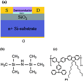 |
| | Fig. 1 (a) The schematic view of the bottom-gate transistor configuration. The chemical structures of (b) hexamethyldisilazane (HMDS) and (c) poly(N-(4-(9,9-dioctyl-fluoren-2-yl)phenyl)-N,N′,N′-triphenyl-l,4-phenylenediamine) (P1). | |
3. Results and discussion
The transmission spectrum of P1 in the wavelength region of 300–800 nm is shown in Fig. 2. The corresponding spectra of P3HT and bare glass are provided as well for comparison. It is clear that the polymer P1 maintains high transmittance (>80%) in the region of 450–800 nm, which is comparable with bare glass. The transmittance of P1 reduced to around 60% at 400 nm and then decreased further in the UV region. The result suggests that P1 is a wide bandgap polymer, which exhibits high transparency in the visible region. In contrast, P3HT has very pronounced reduction of transmittance (<10%) in the visible region (450–600 nm). The inset of Fig. 2 shows a photograph of P1 and P3HT films spin-cast on glass substrates individually, and bare glass for visual comparison. It is evident that the P1 film shows very high transparency as compared with the P3HT film. As a result, P1 would be a suitable polymer for transparent electronics.
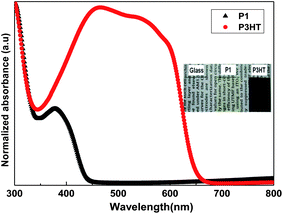 |
| | Fig. 2 The UV-Vis transmission spectra of P1 and P3HT thin films on glass, and bare glass. The inset shows the photograph of bare glass, and P1 and P3HT thin films on glass substrates for visual comparison. | |
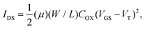
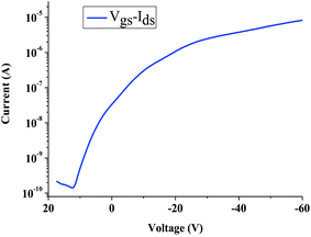
According to a previous report, the polymer P1 reveals a relatively high hole mobility as compared with other conjugated polymer systems by time-of-flight measurements (TOF).21Fig. 3 shows the output characteristics (Ids and Vds) of the transistor with the gate voltage (Vgs) from 0 to −60 V in steps of 10 V. It exhibits p-channel field effect transistor characteristics in our device. The accumulation of holes forms a conductive p-channel, when the negative Vgs is applied to the gate electrode. A saturation drain current with increasing drain voltage (Vds) is obtained, even when the gate voltage is zero. The curves shown in Fig. 3 exhibit qualitatively ideal transistor characteristics using P1 material as an active layer. The voltage transfer characteristic (VTC) of drain current versus gate voltage at Vds = −60 V is shown in Fig. 4. The VTC gives the current response ability versus gate voltage of transistors. The device with P1 material as the channel layer has an on–off ratio of about 5.8 × 10⁴. Further assessment of OTFT current–voltage characteristics allows the estimation of the effective channel mobility. The field effect mobility μ of the fabricated device can be estimated using the equation:22–25
| |  | (1) |
where
W and
L are the width and length of the channel,
COX is the insulator capacitance per unit of the gate dielectric, and
VT is the threshold voltage. The mobility was extracted from the saturation regime at a drain–source voltage of −60 V. The calculated value of the mobility for the transistor is 0.95 × 10
−2 cm
2 V
−1 s
−1, which to the best of our knowledge suggests that P1 possesses the highest field effect mobility among transparent
polymers for transistors.
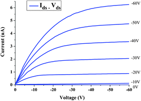 |
| | Fig. 3 Drain current–voltage characteristic of a P1-based OTFT under different working voltages. | |
 |
| | Fig. 4 Transfer characteristics of a P1-based OTFT. | |
4. Conclusion
In summary, we have demonstrated a high performance organic thin film transistor based on a novel highly transparent p-type semiconductor polymer P1. Our study suggests that the fabrication of organic transistors via a solution process by utilizing P1 provides an excellent opportunity for future transparent flexible electronics.
Acknowledgements
This work was supported by the National Science Council and Ministry of Education of the Republic of China.
References
- B. Crone, A. Dodabalapur, Y. Y. Lin, R. W. Filas, Z. Bao, A. LaDuca, R. Sarpeshkar, H. E. Katz and W. Li, Nature, 2000, 403, 521 CrossRef CAS.
- T. Someya, H. E. Katz, A. Gelperin, A. J. Lovinger and A. Dodabalapur, Appl. Phys. Lett., 2002, 81, 3079 CrossRef CAS.
- J. H. Jou, M. H. Wu, S. M. Shen, H. C. Wang, S. Z. Chen, S. H. Chen, C. R. Lin and Y. L. Hsieh, Appl. Phys. Lett., 2009, 95, 013307 CrossRef.
- M. Kano, T. Minari, K. Tsukagoshi and H. Maeda, Appl. Phys. Lett., 2011, 98, 073307 CrossRef.
- G. Wang, T. Hirasa, D. Moses and A. J. Heeger, Synth. Met., 2004, 146, 127 CrossRef CAS.
- I. M. Graz and S. P. Lacour, Appl. Phys. Lett., 2009, 95, 243305 CrossRef.
- J. F. Chang, B. Sun, D. W. Breiby, M. M. Nielsen, T. I. Sölling, M. Giles, I. McCulloch and H. Sirringhaus, Chem. Mater., 2004, 16, 4772 CrossRef CAS.
- Hyejin Kim, Bokyung Yoon, Jinwoo Sung, Dae-Geun Choi and Cheolmin Park, J. Mater. Chem., 2008, 18, 3489 RSC.
- P. Y. Lo, P. W. Li, Z. W. Pei, J. Hou and Y. J. Chan, IEEE Electron Device Lett., 2009, 30, 629 CrossRef CAS.
- K. J. Baeg, D. Khim, D. Y. Kim, J. B. Koo, I. K. You, W. S. Choi and Y. Y. Noh, Thin Solid Films, 2010, 518, 4024 CrossRef CAS.
- E. Orgiu, N. Crivillers, J. Rotzler, M. Mayor and P. Samorı, J. Mater. Chem., 2010, 20, 10798 RSC.
- R. E. Presley, D. Hong, H. Q. Chiang, C. M. Hung, R. L. Hoffman and J. F. Wager, Solid-State Electron., 2006, 50, 500 CrossRef CAS.
- H. H. Hsieh and C. C. Wu, Appl. Phys. Lett., 2007, 91, 013502 CrossRef.
- Y. J. Cho, J. H. Shin, S. M. Bobade, Y. B. Kim and D. K. Choi, Thin Solid Films, 2009, 517, 4115 CrossRef CAS.
- Y. J. Lin, Y. C. Li, T. C. Wen, L. M. Huang, Y. K. Chen, H. J. Yeh and Y. H. Wang, Appl. Phys. Lett., 2008, 93, 043305 CrossRef.
- Y. C. Li, Y. J. Lin, C. Y. Wei, Z. X. Lin, T. C. Wen, M. Y. Chang, C. L. Tsai and Y. H. Wang, Appl. Phys. Lett., 2009, 95, 163303 CrossRef.
- L. A. Majewski, M. Grell, S. D. Ogier and J. Veres, Org. Electron., 2003, 4, 27–32 CrossRef CAS.
- J. Veres, S. D. Ogier, S. W. Leeming, D. C. Cupertino and S. Mohialdin Khaffaf, Adv. Funct. Mater., 2003, 13, 199–204 CrossRef CAS.
- J. Veres, S. Ogier and G. Lloyd, Chem. Mater., 2004, 2004, 4543–4555 CrossRef.
- S. C. Lim, S. H. Kim, J. H. Lee, M. K. Kim, D. J. Kim and T. Zyunga, Synth. Met., 2005, 148, 75 CrossRef CAS.
- W. H. Chen, K. L. Wang, W. Y. Hung, J. C. Jiang, D. J. Liaw, K. R. Lee, J. Y. Lai and C. L. Chen, J. Polym. Sci., Part A: Polym. Chem., 2010, 48, 4654 CrossRef CAS.
- F. C. Chen, Y. S. Lin, T. H. Chen and L. J. Kung, Electrochem. Solid-State Lett., 2007, 10, H186 CrossRef CAS.
- L. Zhen, W. Guan, L. Shang, M. Liu and G. Liu, J. Phys. D: Appl. Phys., 2008, 41, 135111 CrossRef.
- P. D. Kazarinoff, P. J. Shamburger, F. S. Ohuchi and C. K. Luscombe, J. Mater. Chem., 2010, 20, 3040 RSC.
- L. Miozzo, A. Yassar and Gi. Horowitz, J. Mater. Chem., 2010, 20, 2513 RSC.
|
| This journal is © The Royal Society of Chemistry 2012 |
Click here to see how this site uses Cookies. View our privacy policy here.