DOI:
10.1039/C1JM13766B
(Paper)
J. Mater. Chem., 2012,
22, 192-198
Film thickness controllable wet-imprinting of nanoscale channels made of conducting or thermoresponsive polymers
Received
5th August 2011
, Accepted 16th September 2011
First published on 24th October 2011
Abstract
We report the fabrication of structured polymer films via a novel imprinting routine, which additionally allows for entire surface coverage by an underlying homogeneous polymer film. The imprinting method is based on an inverted micromolding in capillaries (MIMIC) approach and in combination with master molds made of bisphenol-A–polycarbonate (PC) sample sizes of up to 20 × 30 mm2 were perfectly structured. Nanoscopic channel structures made of the conducting poly(3,4-ethylenedioxy-thiophene):poly(styrene sulfonate) (PEDOT:PSS) and the thermoresponsive poly(N-isopropylacrylamide) (PNIPAM) also prove the wide application possibilities of this structuring method. For PEDOT:PSS structures the film thickness of the homogeneous supporting polymer layer can be controlled between 0 and 80 nm by an externally applied pressure during imprinting. In addition, conducting polymer blend films as they are used for organic solar cells have a reduced optical reflection if spin cast onto such structured PEDOT:PSS films. For channel structures made of PNIPAM it is shown that their macroscopic optical grating effect responds to the environmental humidity. Due to water inclusion in the PNIPAM network unifying of adjacent channels occurs already in the early stages of the swelling process and results in a homogeneous polymer film. Finally a first batch processing device for the structuring routine is demonstrated, which also guarantees constant lift-off conditions.
Introduction
Due to their immense chemical variety and the resulting application possibilities structured polymer films are in the focus of worldwide research. Especially the easy fabrication of organic structures on mesoscopic and even nanoscopic scale is of utmost interest.1 Therefore different fabrication routines have been invented to suit the individual needs depending on the size of the imprinted structures, the materials used, and the overall area to be covered. Common methods used for the assembly of polymeric microstructures are for example photolithography,2molding,3 and embossing.4 However, many of these methods are limited to planar substrates, rigid master structures, and only a few specialized polymers.5 In addition to these top-down methods block copolymers6 and polymer sphere arrays7 have shown their suitability to act as promising platforms for the fabrication of nanostructured materials. In general, organic materials are due to their solution processability very promising candidates for a cost-effective production of future flexible electronic devices on an industrial scale e.g. via different printing methods.8 Nevertheless up to now most of the different structuring routines for polymer thin films include a treatment step at high temperatures or under high-intensity UV-radiation. Such high energy steps are on the one hand necessary to cure functionalized polymers or on the other hand to soften the material by heating it above its glass transition temperature (Tg). Therefore still new and simple ways to fabricate microstructures have to be developed in order to fulfil the demand of large area polymeric microstructures at low costs and under repeatable conditions. One possible approach is the MIMIC-method (micromolding in capillaries).9 As other methods like microcontact-printing10 or replica-molding11 also this routine belongs to the group of soft lithography and has great advantages: no exposure to high-energy radiation, fabrication at low-costs, and a direct replication of the master structures. Since many novel polymers are sensitive to temperature and pressure, this method based on solution casting principles is very well suited for organic microstructures. Up to now molds based on poly(dimethylsiloxane) (PDMS) are widely used for different imprinting techniques even though they struggle with the disadvantage of being elastic under pressure (elastic modulus ≈ 2–4 MPa). Because of that still stiff inorganic molds produced from silicon, fused silica or amorphous metals allow for the smallest imprint patterns (down to ∼10 nm).12 Since such robust mould materials are crucial for small structure sizes a new class of rigiflex lithography was introduced.13 These bilayer molds manage the bridge between hard and soft lithography combining the advantages of both methods: high resolution and good flexibility. However, the fabrication of such bilayer master structures is rather complicated.
In this article we report a new imprinting routine, which is suitable for various application-oriented polymeric materials and allows a distinctive control of the film thickness. Therefore after introducing the structuring method the results for two different polymer types and their application possibilities are presented. After illustrating a fabrication tool as it can be used for a possible batch production the article ends with a short conclusion.
Results and discussion
Imprinting technique
The novel imprinting routine combines the principles of micromolding in capillaries with the advantages of a semi-flexible mold as a cost effective competitor against other imprinting techniques. The material of choice is a commercially available mold made from bisphenol-A–polycarbonate (PC). Compared to PDMS, PC has a higher Young's modulus (E = 2–2.4 GPa), a Tg of 150 °C, and it shows good chemical resistance against diluted acids. It can also resist higher tensile strengths (σt (PC) ≈ 60 MPa vs. σt (PDMS) ≈ 2 MPa) and hence its high stiffness in combination with its known capability of undergoing plastic deformations by keeping its original shape makes it an ideal candidate also for lithographic approaches. Due to the excellent structure transfer from hard master structures to PC at high replication fidelities it is a standard material for thermal nanoimprinting of nanoscopic structures.14 Concerning the longtime stability of master molds it was recently investigated that an increased elastic modulus of the master structures also increases their reusability for multiple imprinting processes.15
For a standard MIMIC-process the master is put on a support and the polymer solution is spread around its edges. In our approach an inverted design is chosen. The mold with the desirable inverted structure is covered with polymer solution and the substrate is placed upside-down on the polymer solution. Due to the capillary forces the channels are filled and the desired structures develop during solvent evaporation. However, especially for molds with nanoscopic structure features, good wetting properties and a low viscosity of the polymer solution are desired to completely fill the mold structures. By changing the order of the mold and the support—support on mold instead of mold on support—we are able to regulate the thickness of a continuous polymer layer underneath the microstructures. A similar inverted approach was already shown for different inorganic oxide structures, which however still require a posterior heat treatment step to undergo the sol–gel transition.16 Since for the inverted experimental set-up a steady material support from the underlying solution layer is guaranteed the microstructures are completely filled and hence a perfect replication of the master structure is achieved.
Fig. 1 shows the schematic procedure of the imprint. The PC mold has to be horizontally aligned and a given amount of polymer solution is spread on the master depending on the solvent type and the substrate material (values are given in the Experimental section). By gently putting the solid substrate on top of the solution a homogeneous layer of solution is sandwiched between substrate and mold. During the solvent evaporation step an external pressure can be applied to control the total film thickness of the polymer structures and the homogeneous polymer layer underneath. Therefore additional weights in size of the substrate are most suited for uniform imprints. They have the advantage to self-regulate the changing substrate height during solvent evaporation and, hence, guarantee a constant pressure. After the solvent has evaporated completely and the mold structures are filled perfectly with solid polymer, the lift-off takes place. Due to the good flexibility of the PC mold (flexural modulus of 2200 MPa17) the master can be easily bent beneath the substrate leaving an uniformly structured polymer film on the solid support. In general, a perfect lift-off is only possible for systems which allow a stronger surface adhesion of the dry polymer film to the applied substrate than to the master mold. As it is shown in the following for two different examples PC in many cases fulfils this restriction. This straight procedure makes our approach appropriate for a possible application in a roll-to-roll fabrication of structured organic materials as it has been already realized on flexible PET substrates by nanoimprint lithography.18 Further information on this aspect is given below. The time necessary for the imprinting process can be controlled by different environmental conditions such as the surrounding solvent vapor pressure or a change in temperature. Since the polymeric structures develop from solution there is a limitation for the solvents used in order not to corrode the mold. Although PC can be dissolved in different halogens, it shows a good chemical resistance against alcohols, halogenated hydrocarbons, and water. Thus this routine allows an easy fabrication of microstructures from multiple different polymeric components. In the following, two examples based on the conducting poly(3,4-ethylenedioxythiophene):poly(styrene sulfonate) (PEDOT:PSS) and the temperature-responsive poly(N-isopropylacrylamide) (PNIPAM) are presented.
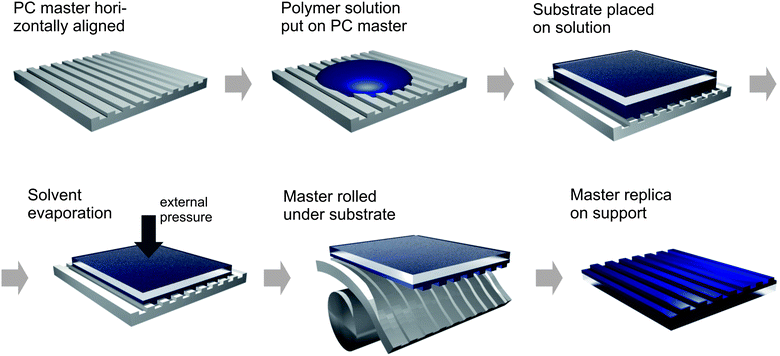 |
| | Fig. 1 Schematic procedure for the formation of patterned polymer films based on semiflexible polycarbonate master molds. | |
Structures made of PEDOT:PSS
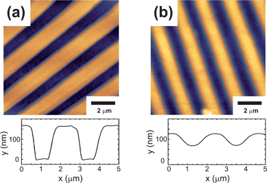
PEDOT:PSS is widely used for organic electronics as an interlayer between electrode and active organic layer.19,20 It is as well a promising candidate for transparent electrodes replacing e.g. conducting indium tin oxides (ITO).21 For polymer light emitting diodes patterned PEDOT:PSS anodes with channel structures of 100 μm have been already fabricated via a solution based imprinting method using a PDMS mold.22 In addition, smaller structure sizes have been reached utilizing a time consuming multiple-step photolithography method based on novel photoresists.23Fig. 2(a) shows the topography atomic force microscopy data of imprinted channels according to the fabrication routine from above and the corresponding profile cut taken perpendicular to the channel structures. The shape of the channels is defined by a spacing of 0.8 μm, a periodicity of 2 μm, and a total height of 175 nm, which match well to the negative structure of the master mold. On hard glass or silicon substrates channel structures with an overall size of up to 20 × 30 mm2 have been fabricated homogeneously. Since the area was limited by the size of the mold it can be expected that larger substrates as well can be imprinted using the same technique. As already mentioned a key parameter for a successful imprinting is the surface adhesion of the polymer and the polymer solution to the substrate. For a perfect replica it is necessary to guarantee a full coverage of the substrate by the polymer solution during the imprinting. Therefore the contact angles between the PEDOT:PSS solution and the different substrates are an appropriate measure: θc (glass) = 8°, θc (PC) ≈ 91°, and θc (textured PC) ≈ 92°. The smaller contact angle between the solution and solid support indicates a complete substrate coverage and hence guarantees a uniform polymer layer underneath the final imprinted structures. Since the contact angle of the solution on the PC mold is ∼91° it can be expected that the capillary forces are very small and that the channels are not filled without any additional pressure. The applied aqueous PEDOT:PSS solution had a total polymer concentration of 1.3 wt% (more details are found in the Experimental section). By varying the concentration between 0.3 and 2.6 wt% it was found that low polymer concentrations lead to incomplete structures due to a lack of polymeric material. In contrast, a mean polymer concentration of 1.3 wt% was best suited for reproducible and well controllable structured films.
 |
| | Fig. 2
AFM topography images and the corresponding profile plots of (a) pure imprinted PEDOT:PSS channels and (b) coated channel structures. The pristine structures show a rectangular shape, whereas additional spin coating with a polymer blend layer leads to a wavy surface. | |
For actual electronic devices PEDOT:PSS is widely used in combination with photoactive polymers in order to build organic light emitting diodes or solar cells, which already reach power conversion efficiencies of over 7%.24Fig. 2(b) shows the surface of such a photoactive polymer blend film based on poly(9,9-dioctylfluorene-co-benzothiadiazole) (F8BT) and poly(3-hexylthiophene) (P3HT) spin cast on a structured PEDOT:PSS layer (see Fig. 2(a)). In comparison to the pure PEDOT:PSS channels, which have a peak-to-valley ratio of 175 nm, the corresponding value for the coated sample is reduced to 55 nm. Similar wavy surface modifications, which were achieved via direct soft lithography, already led to an improved overall power conversion efficiency of organic solar cells.25 As it can be seen in Fig. 3 the almost sinusoidal surface additionally decreases the optical reflection along the incoming plane depending on the wavelength of the incoming light. The reflectivity of the P3HT:F8BT blend film is not only lowered by a factor five, also additional reflection characteristics due to the wavy surface are introduced. Nevertheless for application of such structured surfaces in electronic devices a continuous PEDOT:PSS layer underneath the imprinted structures which covers the whole substrate is crucial. This is the only way to fully utilize the electron blocking or hole injecting characteristics of the PEDOT:PSS and to avoid short-circuit faults between bottom and top electrodes. Since such intermediate layers are in general highly important for the device efficiency also other novel materials are currently investigated as hole transport and electron blocking layers.26Fig. 4 shows a scanning electron microscopy (SEM) image of such a channel structure with an overall film thickness of 250 nm taken at an incident angle of 50°. Since the imprinted channels have a height of 175 nm the homogeneous layer thickness is around 75 nm, which is also in good agreement with the SEM image (Fig. 4). The increased contrast between the polymer surface and the film profile due to a thin vertically evaporated gold layer reveals a homogeneous polymer coverage. Explicitly also the area between the fabricated structures shows a smooth PEDOT:PSS film.
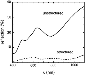 |
| | Fig. 3
Reflectivity
spectra of P3HT:F8BT polymer blend films spin cast on planar and structured PEDOT:PSS films. For the structured film the reflectivity along the sample normal is reduced strongly. | |
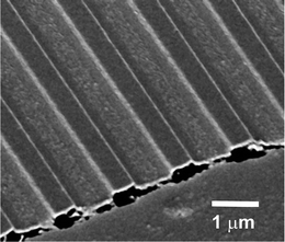 |
| | Fig. 4 The side view SEM image of the channel structures reveals a homogeneous polymer layer underneath. | |
Because PEDOT:PSS is known to absorb optical light27 a good control of its film thickness is crucial for any optoelectronic applications. Fig. 5(a) shows the total film thickness of the structured films with respect to the applied pressure during the solvent evaporation step. Interestingly an increasing film thickness is observed for enhanced pressures. A possible explanation for this counterintuitive dependence is based on a pressure induced higher degree of entanglement between the polymer chains. It can be speculated that during the evaporation step a more entangled polymer network hinders the migration of the polymer chains. Therefore only the smaller solvent molecules can diffuse to the substrate edges and the long rod-like polymer chains are trapped. For higher pressure this effect can even be increased and hence lead to thicker polymer films. However, additional experiments involving other polymer types would be necessary to fully understand this behavior. In addition, the quality of the imprinted channel structures is given by the total film thickness. It has been found that for overall PEDOT:PSS film thicknesses smaller than 175 nm, which is the actual channel depth of the master mold, the imprinted structures are incomplete. Fig. 5(b) shows an optical micrograph image of such a defective film and Fig. 5(c) shows a homogeneously imprinted film with an increased total film thickness. It is seen that thin films are not fully covered and have fractured and incomplete channel structures. A homogeneous polymer layer connecting the imprinted structures (as seen in Fig. 4) is not present and the obtained channel structures are freestanding. For the incomplete films the missing parts of the polymeric channel structures remain in the master mold during the lift-off. In additional experiments imprinted PEDOT:PSS films with an overall film thickness of up to ∼1 μm could be fabricated by modifying the polymer concentration. As indicated already by the optical microscopy image in Fig. 5(c), imprinted PEDOT:PSS films with an overall thickness of above 180 nm show a uniform channel spacing over a macroscopic area. In addition, AFM data taken at multiple different spots of a standard 20 × 20 mm2 sample reveal also identical channel dimensions.
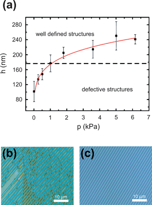 |
| | Fig. 5 (a) The overall film thickness is plotted with respect to the applied pressure during imprinting. The optical micrographs show (b) incomplete structures for film thicknesses below 175 nm and (c) perfect imprints for thicker films. | |
As mentioned in the Introduction one of the main advantages of organic electronics lies in their mechanical flexibility. Therefore Fig. 6 proves that the same imprinting technique is not limited to solid supports but can also be applied on flexible PET foils covered with ITO. Based on Bragg's principles the observable rainbow spectrum is due to interference effects of light reflected from the channel structure. It has to be noted that different surface properties of other substrate materials might require modified experimental conditions. However, since for ITO and glass substrates good imprinting results were achieved under identical experimental conditions, the structuring routine can be easily adapted to other sample systems (additional information about sample preparation is given in the Experimental section).
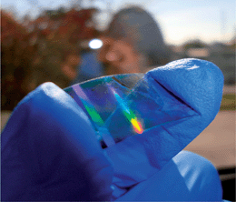 |
| | Fig. 6 Imprinted PEDOT:PSS channels applied to flexible PET substrates covered with ITO show an optical grating effect. | |
Structures made of PNIPAM
The presented inverted imprinting approach based on PC molds is not restricted to conducting polymers but can also be applied to other polymer types e.g. temperature responsive hydrogels. As an example PNIPAM dissolved in water is known to undergo a reversible lower critical solution temperature (LCST) transition accompanied with a tremendous change in volume.28,29 Due to its LCST at 33 °C PNIPAM has been in focus for hydrogen-bonded layer-by-layer materials acting as temperature-triggered release layers for controlled drug delivery systems.30 For application in nanocomposites hydrogel networks support the in situ controlled growth of gold nanorods by regulating the reduction rate of gold ions.31 The preparation of thin PNIPAM films and the swelling kinetics of these films have been studied already32 and it is known that such films are very sensitive to high humidity environmental conditions. Fig. 7 shows the swelling and the antithetic shrinkage process at room temperature of a 83 nm thick PNIPAM film. Due to water uptake in a saturated environment the film thickness can expand to values three times higher as its original film thickness (dswell/d0 ≈ 3). Whereas the swelling process happens on a time scale of hours (maximum film thickness after 300 min), the PNIPAM film releases the previously incorporated water almost instantaneously after a sudden decrease of humidity. In combination with additional physical properties as they can be introduced by structuring the high sensitivity of PNIPAM to humidity can be the essential key for novel ‘smart’ applications. In Fig. 8optical microscopy images display the evolution of PNIPAM channels, if they are exposed to saturated water vapor. They have been fabricated according to the presented routine and since the same PC mold as for the PEDOT:PSS channels was used the structure dimensions are similar as compared to Fig. 2(a). In order to focus on the swelling of the channel structures and not of the homogeneous PNIPAM layer underneath free-standing structures are chosen. Therefore the polymer was dissolved at a concentration of 28 mg ml−1. Higher concentrations of 36 mg ml−1 result in imprints with a homogeneous surface coverage. Interestingly, a partial unification of adjacent channels can be found happening already in the early stages of the swelling process. For the maximum water uptake the swollen film buries the fabricated structures and even leads to a homogeneous surface coverage. The rapid decrease of film thickness in the swollen-dry transition is indicated by the color change in the optical microscopy images. As for the PEDOT:PSS grating in Fig. 6 a similar physical color effect is also seen for the untreated PNIPAM channels (inset: Fig. 8, 0 min). Since this phenomenon is depending on the periodicity and the shape of the structures a smooth transition from an intense rainbow spectrum to a featureless surface reflection (inset: Fig. 8, dry) can be observed. Such water vapor sensitive gratings have great potential not only for optical but also for medical applications, since this structured ‘multitasking-smart’ material reacts to certain manually controlled environmental variations by film thickness adaptations in combination with a change of its optical properties.
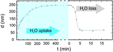 |
| | Fig. 7 Film thickness changes of homogeneous PNIPAM thin films by modification of ambient conditions due to H2O uptake and loss. The solid line acts as a guide to the eye. | |
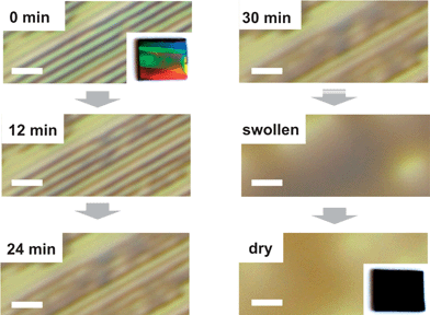 |
| | Fig. 8 The optical microscopy images show the swelling and unifying of single PNIPAM-channels due to H2O inclusion (scale bar depicts 5 μm). The inset photographs illustrate the optical grating effect of the sample before (0 min) and after water vapor treatment (dry). | |
Batch-processing set-up
For a large scale fabrication of such organic optical or electronic devices the roll-to-roll approach is very promising.33 Therefore Fig. 9 shows a schematic illustration of a lab-scale fabrication device as it was used for the introduced structuring routine. It was designed in such a way that it could be adapted for a future roll-to-roll process. The set-up includes two deflection pulleys with a diameter of 130 mm and an additional tension pulley, which is necessary to guarantee a strong tension of the tooth belt and hence a good alignment. The bisphenol-A–polycarbonate master structure can be mounted on the metal-reinforced rubber tooth belt by simply sticking for the thinner or screwing for the thicker PC master structures (total master thickness varied between 0.2 and 1.2 mm). Since the fabrication routine is based on solution casting principles a horizontal alignment of the master structure is absolutely necessary. Therefore the set-up is equipped with a leveling stage, on which the sample remains during the solvent evaporation step (Fig. 9, see 1). Since this is the time limiting step during sample production, the environmental humidity and temperature can be modified in order to speed up the solvent evaporation (see also the Experimental section). For the sample lift-off the master is moved towards the deflection pulley and due to the bending of the master structure along the curvature of the deflection pulley the sample substrate is automatically lifted off. For the lift-off a rotational speed of the deflection pulley of 10 deg s−1 was appropriate for a successful substrate separation. This corresponds to a processing speed of 40 m h−1 for the lift-off step. Afterwards the sample could be easily picked up with an additional pick-up pulley and transported to a following production step (Fig. 9, see 2). An additional advantage of this set-up is that it not only allows for a batch production of structured polymer films but it as well guarantees constant peel-off conditions. These constant lift-off conditions also result in high reproducibility rates on a lab scale for standard structured PEDOT:PSS samples with a total film thickness of above 180 nm (see also Fig. 5(a) and (c)). However, a precise control of the environmental conditions (temperature and humidity) and the applied external pressure is crucial for perfect reproducibility.
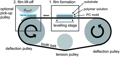 |
| | Fig. 9 Schematic illustration of a batch-processing device as applied for our imprinting routine. During the film formation due to solvent evaporation (see 1) the sample is supported by an additional leveling stage. For the sample lift-off (see 2) the master structure is bent along the curvature of the deflection pulley. | |
Conclusion
A modified imprinting routine has been introduced and its application was shown exemplary for conducting and thermoresponsive polymers. Due to its very well suited mechanical properties BPA–PC is advantageous as a mold material: it guarantees high resolution imprints in combination with a flexibility suited for direct application in roll-to-roll production. In comparison to the standard MIMIC experimental procedure in our approach the substrate is put on the mold, which is covered with polymer solution beforehand. This inverted order allows for the fabrication of nanostructures on top of a homogeneous polymeric layer which is especially interesting for optoelectronic devices as e.g. solar cells or light emitting diodes. For such applications the conducting PEDOT:PSS polymer is widely used and it was shown that structured PEDOT:PSS films can be easily fabricated not only on solid supports but also on flexible ITO covered PET foils. In addition, the thickness of the homogeneous PEDOT:PSS layer underneath the structures can be controlled by an applied external pressure during the solvent drying phase. Besides conducting structures also thermoresponsive optical gratings made of PNIPAM were imprinted via the same routine. By exposing them to water vapor a tunable optical grating effect can be observed, which is interesting for future structured smart materials. All in all the presented imprinting routine has proven its potential as a low-cost batch processing technique for structured polymer thin films with widespread application possibilities.
Experimental
The PEDOT:PSS (Sigma Aldrich) was an aqueous solution with a polymer concentration of 0.8 wt% of PEDOT and 0.5 wt% of PSS. Before use the solution was treated in an ultrasonic bath for 10 min at room temperature and filtered directly on the mold using a polytetrafluorethylene filter (PTFE, 5 μm). The PNIPAM was synthesized by the group of A. Laschewsky at the University of Potsdam. Its molecular weight was 57![[thin space (1/6-em)]](https://www.rsc.org/images/entities/char_2009.gif) 000 g mol−1 and it was dissolved in deionized water at a concentration of 28 g l−1. The glass substrates were acidic precleaned for PEDOT:PSS and base cleaned for PNIPAM.34 The flexible ITO covered PET foils were purchased from Solaronix (PETITO 175-60) and cleaned in a sequence of ethanol, acetone, and isopropanol before nitrogen blow-drying. The bisphenol-A–polycarbonate (PC) molds are commercially available on a large scale or custom-made. For the standard samples shown in this manuscript a PC mold with a thickness of 1 mm was applied. Imprinting was performed for 48 to 96 h in a horizontally aligned closed container (relative humidity, RH = 70%) or for 24 h at standard conditions (RH = 35%). The samples were kept at room temperature (RT = 23 °C) during processing. However, higher processing temperatures of 40 °C have already indicated faster sample preparation rates. For the imprint of a standard sample size of 20 × 20 mm2 a total solution volume of 0.25 ml was used for both polymers. The optical reflectivity measurements were carried out on a Lambda 35 UV/Vis spectrometer (PerkinElmer). Contact angles were measured with a Dataphysics OCA20 set-up. The atomic force microscopy images were taken in non-contact mode (ULTRAObjective, Surface Imaging Systems GmbH) and the radius of the tip was small in comparison to the measured structures. The overall thicknesses of the PEDOT:PSS films imprinted at different external pressures were determined with a Dektak 3030 from Veeco. The corresponding measurement errors are given by the standard deviation of multiple measurements on different sample positions. The film thickness changes of the spin coated PNIPAM film were measured in situ using a Filmetrics F20-UV white light interferometer. Optical microscopy images were taken on Zeiss Axiolab and Zeiss Axio Imager.A1m and scanning electron microscopy images on a Zeiss NVision40.
000 g mol−1 and it was dissolved in deionized water at a concentration of 28 g l−1. The glass substrates were acidic precleaned for PEDOT:PSS and base cleaned for PNIPAM.34 The flexible ITO covered PET foils were purchased from Solaronix (PETITO 175-60) and cleaned in a sequence of ethanol, acetone, and isopropanol before nitrogen blow-drying. The bisphenol-A–polycarbonate (PC) molds are commercially available on a large scale or custom-made. For the standard samples shown in this manuscript a PC mold with a thickness of 1 mm was applied. Imprinting was performed for 48 to 96 h in a horizontally aligned closed container (relative humidity, RH = 70%) or for 24 h at standard conditions (RH = 35%). The samples were kept at room temperature (RT = 23 °C) during processing. However, higher processing temperatures of 40 °C have already indicated faster sample preparation rates. For the imprint of a standard sample size of 20 × 20 mm2 a total solution volume of 0.25 ml was used for both polymers. The optical reflectivity measurements were carried out on a Lambda 35 UV/Vis spectrometer (PerkinElmer). Contact angles were measured with a Dataphysics OCA20 set-up. The atomic force microscopy images were taken in non-contact mode (ULTRAObjective, Surface Imaging Systems GmbH) and the radius of the tip was small in comparison to the measured structures. The overall thicknesses of the PEDOT:PSS films imprinted at different external pressures were determined with a Dektak 3030 from Veeco. The corresponding measurement errors are given by the standard deviation of multiple measurements on different sample positions. The film thickness changes of the spin coated PNIPAM film were measured in situ using a Filmetrics F20-UV white light interferometer. Optical microscopy images were taken on Zeiss Axiolab and Zeiss Axio Imager.A1m and scanning electron microscopy images on a Zeiss NVision40.
Acknowledgements
We thank Prof. Dr A. Laschewsky for synthesizing the PNIPAM. The authors also thank M. Rawolle for her support with the SEM. The financial support by DFG in the priority program SPP1259 (MU1487/8) and by BMBF project 05KS7W01 is gratefully acknowledged.
References
- H. D. Tran, D. Li and R. B. Kaner, Adv. Mater., 2009, 21, 1487 CrossRef CAS.
-
W. M. Moreau, Semiconductor Lithography: Principles and Materials, Plenum Press, New York, 1988 Search PubMed.
- J. F. Dijksman, Philips Tech. Rev., 1989, 44, 212 Search PubMed.
- S. Y. Chou, P. R. Krauss and P. J. Renstrom, Science, 1996, 272, 85 CrossRef CAS.
- E. Scheler and P. Strohriegl, J. Mater. Chem., 2009, 19, 3207 RSC.
- J. Bang, U. Jeong, D. Y. Ryu, T. P. Russell and C. J. Hawker, Adv. Mater., 2009, 21, 4769 CrossRef CAS.
- H. Park, S. Choi, J.-P. Lee and S. Park, J. Mater. Chem., 2011, 21, 11996 RSC.
- F. C. Krebs, Sol. Energy Mater. Sol. Cells, 2009, 93, 394 CrossRef CAS.
- E. Kim, Y. Xia and G. M. Whitesides, Nature, 1995, 376, 581 CrossRef CAS.
- A. Kumar and G. M. Whitesides, Appl. Phys. Lett., 1993, 63, 2002 CrossRef.
- Y. Xia, E. Kim, X.-M. Zhao, J. A. Rogers, M. Prentiss and G. M. Whitesides, Science, 1996, 273, 347 CrossRef CAS.
- G. Kumar, H. X. Tang and J. Schroers, Nature, 2009, 457, 868 CrossRef CAS.
- D. Suh, S.-J. Choi and H. H. Lee, Adv. Mater., 2005, 17, 1554 CrossRef CAS.
- F. Zhang and H. Y. Low, Nanotechnology, 2006, 17, 1884 CrossRef.
- D. R. Barbero, M. S. M. Saifullah, P. Hoffmann, H. J. Mathieu, D. Anderson, G. A. C. Jones, M. E. Welland and U. Steiner, Adv. Funct. Mater., 2007, 17, 2419 CrossRef CAS.
- M. J. Hampton, S. S. Williams, Z. Zhou, J. Nunes, D.-H. Ko, J. L. Templeton, E. T. Samulski and J. M. DeSimone, Adv. Mater., 2008, 20, 2667 CrossRef CAS.
- C. K.-Y. Li, Z.-Y. Xia and H.-J. Sue, Polymer, 2000, 41, 6285 CrossRef CAS.
- S. H. Ahn and L. J. Guo, Adv. Mater., 2008, 20, 2044 CrossRef CAS.
- F. C. Krebs, Sol. Energy Mater. Sol. Cells, 2009, 93, 465 CrossRef CAS.
- M. A. Ruderer and P. Müller-Buschbaum, Soft Matter, 2011, 7, 5482 RSC.
- P. A. Levermore, R. Jin, X. Wang, L. Chen, D. D. C. Bradley and J. C. de Mello, J. Mater. Chem., 2008, 18, 4414–4420 RSC.
- P. G. Taylor, J.-K. Lee, A. A. Zakhidov, M. Chatzichristidi, H. H. Fong, J. A. DeFranco, G. G. Malliaras and C. K. Ober, Adv. Mater., 2009, 21, 2314 CrossRef CAS.
- Y. Liang, Z. Xu, J. Xia, S.-T. Tsai, Y. Wu, G. Li, C. Ray and L. Yu, Adv. Mater., 2010, 22, E135 CrossRef CAS.
- T. Granlund, T. Nyberg, L. S. Roman, M. Svensson and O. Inganäs, Adv. Mater., 2000, 12, 269 CrossRef CAS.
- S.-I. Na, S.-S. Kim, J. Jo, S.-H. Oh, J. Kim and D.-Y. Kim, Adv. Funct. Mater., 2008, 18, 3956 CrossRef CAS.
- Y. Sun, M. Wang, X. Gong, J. H. Seo, B. B. Y. Hsu, F. Wudl and A. J. Heeger, J. Mater. Chem., 2011, 21, 1365 RSC.
- L. A. A. Pettersson, S. Ghosh and O. Inganäs, Org. Electron., 2002, 3, 143 CrossRef CAS.
- H. G. Schild, Prog. Polym. Sci., 1992, 17, 163 CrossRef CAS.
- T. Hellweg, C. D. Dewhurst, W. Eimer and K. Kratz, Langmuir, 2004, 20, 4330 CrossRef CAS.
- E. Kharlampieva, V. Kozlovskaya and S. A. Sukhishvili, Adv. Mater., 2009, 21, 3053 CrossRef CAS.
- C. Jiang, Y. Qian, Q. Gao, J. Dong and W. Qian, J. Mater. Chem., 2010, 20, 8711 RSC.
- W. Wang, K. Troll, G. Kaune, E. Metwalli, M. A. Ruderer, K. Skrabania, A. Laschewsky, S. V. Roth, C. M. Papadakis and P. Müller-Buschbaum, Macromolecules, 2008, 41, 3209 CrossRef CAS.
- F. C. Krebs, S. A. Gevorgyan and J. Alstrup, J. Mater. Chem., 2009, 19, 5442 RSC.
- P. Müller-Buschbaum, Eur. Phys. J. E: Soft Matter Biol. Phys., 2003, 12, 443 Search PubMed.
|
| This journal is © The Royal Society of Chemistry 2012 |
Click here to see how this site uses Cookies. View our privacy policy here.