Visible light photochemical activity of heterostructured PbTiO3–TiO2 core–shell particles
Li
Li
,
Yiling
Zhang
,
Andrew M.
Schultz
,
Xuan
Liu
,
Paul A.
Salvador
and
Gregory S.
Rohrer
*
Department of Materials Science and Engineering, Carnegie Mellon University, Pittsburgh, PA, USA. E-mail: gr20@andrew.cmu.edu; Fax: 412 268 7596; Tel: 412 268 2696
First published on 10th May 2012
Abstract
Heterostructured powders composed of microcrystalline PbTiO3 cores coated with nanostructured TiO2 shells were prepared by a sol–gel method. When exposed to visible light (λ > 420 nm), the heterostructured powder degrades methylene blue at a rate 4.8 times greater than PbTiO3, TiO2, or mechanical mixtures of the phases. The rate at which the heterostructured powder degrades methylene blue depends on the processing temperature; samples annealed at 500 °C are the most reactive, even though they do not have the highest surface area. Enhanced degradation rates were not observed for Pb-doped TiO2, indicating that it is the core–shell architecture and not contamination by lead that increases the reactivity. The improved reactivity of microcrystalline-PbTiO3/nanostructured-TiO2 heterostructures in visible light is attributed to visible light absorption in the PbTiO3 core, charge separation at the buried interface between the ferroelectric PbTiO3 and the dielectric TiO2, and dye degradation on the nanostructured TiO2 shell.
1. Introduction
Titania is the most widely studied photocatalytic material.1–3 To enhance its visible light response, it is often doped or used in conjunction with other semiconductors.4–9 Doping is thought to create absorption states in the gap, allowing absorption of lower energy light. Semiconductor junctions can promote charge separation through favorable band alignments and this has the potential to reduce recombination losses. The advantage of semiconductor junctions, in the form of composite or core–shell materials, is that the light absorption and surface reaction steps can be optimized in distinct phases. For example, it has been shown that when titania is coupled to certain oxides with a narrower band gap, its photochemical activity in visible light is enhanced.10,11 Recent work on BaTiO3–TiO2 and SrTiO3–TiO2 microcrystalline-core/nanostructured-shell materials has demonstrated that this hierarchical architecture leads to enhanced water splitting with UV irradiation.12 The present paper is based on a similar composite strategy, but using a visible light absorbing, ferroelectric core (PbTiO3). The composite material described here is distinct from previously studied core–shell materials because it combines a micron-scale, visible light absorbing core that is ferroelectric. The choice of a micron-scale core is to ensure that the volume is sufficient to support full polarization and band bending, which will enhance charge separation. The micro–nano core–shell hierarchical structure presents a new strategy for improving and optimizing the reactivity of photocatalysts. The purpose of this paper is to demonstrate that the visible light photochemical reactivity of titania can be enhanced by supporting it on a ferroelectric PbTiO3 core.The motivation for using a micronsized ferroelectric, visible-light absorbing core derives from the bulk photovoltaic effect observed in semiconducting ferroelectrics.13–15 The internal dipolar field that arises from the spontaneous ferroelectric polarization creates mismatches in the electrochemical potential of electrons at surfaces.16,17 Inoue and co-workers18 showed that the photocatalytic activities of TiO2 and NiO films were enhanced when supported on a poled, ferroelectric LiNbO3 substrate. A similar increase in photocatalytic activity related to domain polarization was observed for ferroelectric Pb(Zr,Ti)O3.19 Those experiments provide direct evidence that the internal dipolar field of a ferroelectric can influence the movement of charge carriers and the photochemical reactivity.
More recently, Giocondi et al.20 showed that photochemical reduction reactions were spatially localized on domains with positive polarization and photochemical oxidation reactions were localized on domains with negative polarization. Burbure et al.21 showed that photochemical reactions on TiO2 films supported by BaTiO3 were also spatially localized and similarly correlated with domain structure. In these TiO2–BaTiO3 heterostructures, the thickness of the film and the orientation relationship between substrate and coating also influenced the photochemical activity of the heterostructure.22,23 Tiwari and Dunn24 recently reviewed the possibility of using polarizable semiconductors to control photochemical reactions. The fact that nanocomposites of ferroelectric BiFeO3 and titania have shown enhanced visible light reactivity supports this concept.8 However, in the BiFeO3/titania work, both phases are nanostructured and the ferroelectric component is unlikely to support full polarization or any significant band bending that can separate charge carriers.25,26 To benefit from any possible advantages imparted by dipolar fields from ferroelectric domains, it is necessary for the ferroelectric to be larger than a critical size in the range of about 200 nanometers.26 Therefore, we have been interested in heterostructured core–shell particles having micronsized cores that absorb light in extended space charge regions, rather than in nanostructured core materials. A recent study of planar heterostructures composed of dense titania supported on visible light-absorbing BiFeO3 demonstrated that electrons generated in the substrate could participate in reduction reactions on the titania surface.10
Taken together, the previous findings suggest that a heterostructured photocatalyst consisting of a ferroelectric, visible light absorbing, microcrystalline core surrounded by a nanostructured titania shell could have enhanced photochemical reactivity in visible light. This paper describes the sol–gel synthesis and characterization of such a material, employing PbTiO3 as the core and nanostructured titania as the shell. The PbTiO3 crystals are relatively large, on the order of microns, while the coating is nanostructured and has a relatively high surface area. The degradation of methylene blue, monitored by optical absorption spectroscopy, is used as a measure of photochemical reactivity. The results show that the heterostructure is more reactive than either of the component phases alone, or mixtures of them, indicating that the enhancement is a result of the particle architecture.
2. Materials and methods
Materials preparation
Commercially available micron-sized PbTiO3 (mc-PbTiO3) (99.9%, Alfa Aesar) was coated with nanostructured TiO2 (ns-TiO2) using a previously reported sol–gel method.8 Titanium tetrabutoxide (TBOT, 99.0%, Acros Organics) was used as a Ti source to fabricate the heterostructure via hydrolysis in the presence of ethanol as a solvent. The procedure starts by mixing 8.6 mL of TBOT with 15 mL of ethanol and stirring for 10 min. To control the hydrolysis rate, 1 mL of 2,4-pentanedione was added to the TBOT/ethanol solution. Another solution was prepared by mixing 20 mL of ethanol, 9 mL of water, and 1 g of mc-PbTiO3. This mixture was sonicated 0.5 h to disperse the powders. The pH was then adjusted to be between 3 and 4 by adding 10 mL acetic acid (≥ 99.7%, Fisher Scientific). The TBOT/ethanol solution was then added drop-wise into the mixture to form the precursor, which was stirred at room temperature for 2 h and then aged at 90 °C in a water bath for 7 h. The product was obtained by collecting the aged powders, washing several times with ethanol, and drying at 80 °C for 24 h. This powder was then calcined in air to crystallize the TiO2 shell. The powders were heated and cooled at 0.5 °C min−1, and annealed for 2 h at 400 °C, 500 °C, or 600 °C. TiO2 was prepared using the same procedure but without the addition of mc-PbTiO3. Pb-doped TiO2 was prepared by dissolving 1 mol% PbO into the precursor solution. As a control experiment, a mechanical mixture of PbTiO3 and TiO2 was prepared (mass ratio 1![[thin space (1/6-em)]](https://www.rsc.org/images/entities/char_2009.gif) :2, consistent with the component percentage of powders prepared by sol–gel method) in ethanol and sonicated at room temperature for 1 h. The mixture was then dried overnight in air at 50 °C.
:2, consistent with the component percentage of powders prepared by sol–gel method) in ethanol and sonicated at room temperature for 1 h. The mixture was then dried overnight in air at 50 °C.
Materials characterization
All powders were analyzed by X-ray diffraction (XRD) using a diffractometer (PANalytical, X’Pert Pro, Philips, Netherlands) equipped with Cu-Kα radiation and operated at 45 kV and 40 mA. A scan rate of 3°/min and a step size of 0.05° were used for all θ–2θ scans. The morphology and microstructure of the powders were characterized with transmission electron microscopy (TEM, F20, TECNAI, Hillsboro, OR) working at an accelerating voltage of 200 kV. Powders were ultrasonically dispersed in methanol and several drops of the suspension were distributed dropwise to the surface of 400 square mesh copper grid coated with a holey carbon support film. N2 adsorption–desorption measurements (Nova 2200e, Quantachrome, FL), used to determine the specific surface area of powders by Brunauer–Emmett–Teller (BET) approach, were performed at 77 K using a multi-point method. Prior to the measurement, all samples were vacuum-degassed for 3 h at 300 °C to remove moisture. The pore size distribution was obtained by Barret–Joyner–Halenda (BJH) model based on the desorption data. Pore volume was measured at the P/P0 = 0.99 point. Diffuse reflectance spectroscopy (DRS) was used to analyze the optical properties of powders. The diffuse reflectance spectra were recorded by a UV-vis spectrophotometer (USB2000, Ocean Optics), equipped with R600-7 reflection probe which is optimized for 250–800 nm region. A PTFE standard with uniform reflectivity between 250 nm and 2000 nm was utilized as the reference.Photochemical reaction setup
The rate of degradation of methylene blue (MB) under visible light irradiation was used as a measure of photochemical activity. A 300 W high pressure mercury lamp was used as the illumination source. An aqueous suspension of 0.3 g of photocatalyst was added to 65 mL of a 10−5 M MB solution and poured into a 100 mL quartz reactor. A UV cutoff filter (Oriel, λ > 420 nm) with 20 cm2 window was placed in front of the quartz reactor to absorb UV light. Prior to irradiation, the suspension was stirred continuously for 2 h in the dark to saturate the powders with the dye solution. The reaction was carried out for five hours and 5 mL samples were removed each hour for absorption measurements. The degradation of methylene blue was evaluated by comparing the intensity of the absorbance peak at 663.89 nm (denoted as C) and the initial intensity (denoted as C0) before irradiation.3. Results
X-ray diffraction patterns of the PbTiO3–TiO2 core–shell particles, the component phases, and Pb-doped titania, all annealed at 500 °C, are shown in Fig. 1. All diffraction peaks could be indexed to the standard patterns of PbTiO3 (JCPDS 78-0299) and anatase TiO2 (JCPDS 46-1237). The pattern for the composite is consistent with a superposition of the two component phases, indicating that almost no reaction occurs between PbTiO3 and TiO2. This observation is consistent with the PbO–TiO2 phase diagram.27 Compared with the diffraction pattern of TiO2, Pb-doped TiO2 shows a small peak at 2θ = 32.4°, which is consistent with the most intense peak in the PbTiO3 pattern, (110). This indicates that the doping exceeded the solubility limit of Pb in TiO2 and that a small amount of the ternary compound was formed. The 2θ peaks at 25.2° and 47.8° are indexed to (101) and (200) planes of anatase, which are marked in Fig. 1 and were used to calculate the lattice parameters of TiO2, Pb-doped TiO2, and TiO2 in the heterostructure. The results are shown in Table 1. Because the ionic radius of Pb is much larger than Ti, it is expected that substitution at the Ti site will cause some lattice expansion. The data in Table 1 indicate a significant lattice expansion occurred for the Pb-doped TiO2 and a slight lattice expansion occurred for the TiO2 in the heterostructures. The expansion of the unit cell indicates that Pb was substitutionally incorporated in the doped titania, with the amount being below the targeted value (owing to the PbTiO3 formation) for the Pb-doped TiO2. The intermediate value of the lattice parameters in the TiO2 coating in the PbTiO3–TiO2 heterostructure indicates only a small amount of Pb interdiffuses to the coating through the interface (being less than the ≈1 mol% in the doped sample).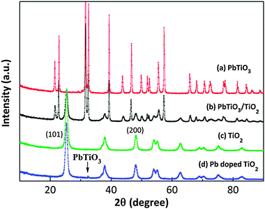 | ||
| Fig. 1 X-ray diffraction patterns of (a) PbTiO3, (b) PbTiO3–TiO2 (c) TiO2 and (d) Pb-doped TiO2 annealed at 500 °C. | ||
| Material | d 101 (Å) | d 200 (Å) | a/Å | c/Å | cell volume/Å3 |
|---|---|---|---|---|---|
| TiO2 | 3.501 | 1.889 | 3.778 | 9.315 | 133.0 |
| H-TiO2 | 3.508 | 1.890 | 3.780 | 9.418 | 134.6 |
| Pb-doped TiO2 | 3.515 | 1.892 | 3.784 | 9.492 | 135.9 |
The TEM images in Fig. 2 illustrate the morphology and microstructure of the heterostructured powders annealed at 500 °C. The image in 2(a) shows a typical particle and the higher resolution image in 2(b&c) shows the interface between the mc-PbTiO3 and ns-TiO2. The PbTiO3 core is electron opaque and appears black in the image. The nanocrystalline TiO2 shell appears as a semi-transparent layer surrounding the core. The partially transparent layer shows a granular contrast that corresponds to titania particles with an approximate diameter of 10 nm, which is consistent with the value of 9 nm calculated based on a Scherer analysis of the breadth of the X-ray peaks shown above. A sharp and clear interface between the micronsized core and the nanostructured coatings can be observed. The thickness of the titania layer is not constant and varies in the range of 50–100 nm, except for the occasional agglomerate attached to the surface.
 | ||
| Fig. 2 TEM images of heterostructured particles composed of mc-PbTiO3 and ns-TiO2 annealed at 500 °C. (a) Low magnification bright field image of entire particle, (b) High magnification bright field image of detail of the PbTiO3–TiO2 interface, (c) HRTEM image of the interface, (d) SAED of TiO2 coating, (e) HRTEM image of the interface after in situ annealing with high energy electron beam. | ||
A high resolution TEM (HRTEM) image taken from the interface is shown in Fig. 2(c). The measured spacing of lattice fringes in the titania coating was 3.5 Å, corresponding to the interplanar distance of the (101) plane of anatase TiO2. The selected-area electron diffraction (SAED) pattern of TiO2 coating is presented in Fig. 2(d). The SAED pattern shows a series of concentric circles rather than sharp bright dots because of the polycrystalline nature of the nano-sized grains. Those diffraction circles were indexed and identified as the planes of tetragonal anatase TiO2.
To demonstrate the influence of high temperature annealing on the nanostructured TiO2 and its interface with the micron sized core, we carried out an in situ annealing experiment in the TEM using a high energy electron beam focusing on the interface with accelerating voltage of 200 kV. A very thin coating area, with two or three TiO2 particle layers, was selected and exposed to a high-energy electron beam. Then we investigated the same region after the annealing with TEM. The interface after in situ annealing is shown in Fig. 2(e). The area in the right side of the interface, related to mc-PbTiO3 core, did not change under annealing. However, coarsened TiO2 grains are clearly observed on the left side of the interface and the size of TiO2 particle has increased from 10 nm to 25 nm. This also leads to a clear decrease in the overall surface area, which is unwanted for catalysis. The observation of fringes (marked with white curve and line) at the PbTiO3–TiO2 interface suggests a direct connection between the two phases, which is beneficial for the electron transfer between the core and shell.
The surface area and pore morphology of mc-PbTiO3–ns-TiO2 annealed at 400, 500, and 600 °C are shown in Table 2. The diameters of the PbTiO3 particles are in the micron range and, therefore, the surface area is small. This result is consistent with the TEM images. The surface areas of the PbTiO3–TiO2 heterostructures decrease on annealing from 117 m2 g−1 at 400 °C to 74 m2 g−1 at 500 °C and 26 m2 g−1 at 600 °C. This is the result of thermally driven consolidation and coarsening, as shown in the in situ TEM experiment.28,29 Based on their measured pore sizes, the mc-PbTiO3–ns-TiO2 and ns-TiO2 prepared by the sol–gel method can be considered mesoporous.
| Material | Processing T/°C | BET surface area (m2 g−1) | Pore volume (cc/g) | Pore radius Dv (r) (Å) |
|---|---|---|---|---|
| ns-TiO2 | 500 | 83 | 0.14 | 25 |
| mc-PbTiO3 | 500 | 2 | 0.01 | N/A |
| mc-PbTiO3–ns-TiO2 | 400 | 117 | 0.19 | 23 |
| 500 | 74 | 0.15 | 28 | |
| 600 | 26 | 0.13 | 55 |
Fig. 3 shows the UV-vis diffuse reflectance spectra of the mc-PbTiO3–ns-TiO2 as well as those of component phases, all annealed at 500 °C. The region between 400 and 450 nm is magnified in the inset to highlight the details near the onset of absorption. The reflectance spectra recorded from the UV-vis spectrometer were converted to absorbance using the Kubelka–Munk function.30 The data in Fig. 3 confirm that TiO2 exhibits little absorbance of light with wavelengths longer than 400 nm. The onset of the absorption of light by PbTiO3 occurs at a longer wavelength because of its smaller band gap energy.31 Specifying a value for the band gap of PbTiO3 is complicated by its anomalous absorption edge32 and, because of this, a wide range of values between 2.75 eV and 3.6 eV can be found in the literature.31–34 Micron-sized PbTiO3 prepared by molten salt methods was reported to have band gap 2.75 eV,31 and this material is apparently similar to the material used here. The absorbance data in Fig. 3 shows that PbTiO3 begins to absorb light at 435 nm, a wavelength consistent with a band gap of 2.85 eV. The absorbtion edge of heterostructured PbTiO3–TiO2 is close to that of the PbTiO3 core material, indicating that the core is the primary photon absorbing phase in the visible region of the spectrum.
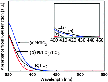 | ||
| Fig. 3 Absorbance data, converted from diffuse reflectance spectra using the K-M function. (a) PbTiO3–TiO2, (b) PbTiO3 and (c) TiO2 annealed at 500 °C. The inset enlarges the absorbance spectra between 400 nm and 450 nm. | ||
mc-PbTiO3–ns-TiO2 annealed at 500 °C and its component phases were used to photochemically degrade methylene blue using visible light (λ > 420 nm). Methylene blue is an organic heterocyclic-dye and is relatively stable against degradation in normal conditions. Photochemical degradation leads to a reduction in absorbance, which correlates to a reduction in concentration. The results are shown in Fig. 4. The data denoted as “blank” is the result of a control experiment carried out in the same way as all of the others, but without an added catalyst. The constant absorbance with time verifies that methylene blue is not homogeneously degraded by visible light under these conditions. Similarly, no degradation is detected for the experiment with microcrystalline PbTiO3 used as the photocatalyst. Recall that this sample has a small surface area compared to the others, so this result does not necessarily mean that PbTiO3 is inert for this reaction, simply that it is not capable of degrading detectible amounts of MB under these conditions. TiO2 by itself shows modest reactivity, even though the absorbance data in Fig. 3 indicates that it is not able to absorb visible light photons. This phenomenon has been reported previously and is referred to as the “TiO2-mediated dye degradation” process.35,36 According to the reported process, TiO2 is not excited by the visible light but provides a pathway for electron transfer from excited dye molecules to oxygen atoms adsorbed on the TiO2 surface. The generation of superoxide radical anion, ˙O2−, and ˙OH radicals on the surface of TiO2 are the primary species responsible for organic dye degradation in these conditions.35,36
 | ||
| Fig. 4 Photochemical dye degradation with PbTiO3–TiO2 annealed at 500 °C and its component phases during irradiation by visible light (λ > 420 nm). Blank refers to data from a control experiment conducted without the addition of a catalyst. The curve from the blank is not visible, because the data from PbTiO3 overlaps it on the horizontal axis. | ||
Compared with the low rates of MB degradation by TiO2, PbTiO3, and physical mixtures of the two phases, the mc-PbTiO3–ns-TiO2 core–shell structure exhibits greater photochemical activity measured by the dye degradation rate. The greater degradation rate is reflected in both the slope of the absorbance versus reaction time curve and by the total amount of dye degraded during the experiment. After 5 h of irradiation, the concentration of MB in the solution decreased to 20% of its initial concentration. The time evolution of the dye concentration can be reasonably accounted for by a pseudo-first-order model, represented by the following equation.37–39
| ln(C0/C) = Kappt | (1) |
Fig. 5 compares the dye degradation rates of mc-PbTiO3–ns-TiO2 annealed at 400 °C, 500 °C, and 600 °C. The results of the dye degradation experiment using Pb-doped TiO2 are also shown in Fig. 5. The results indicate that the annealing temperature influences the photochemical activity of mc-PbTiO3–ns-TiO2. It is noteworthy that the photochemical activity of these heterostructured powders is not simply related to the surface area. The sample annealed at 500 °C degrades MB at the highest rate, even though it does not have the largest surface area. The powder annealed at 600 °C exhibits the lowest reactivity among the heterostructured mc-PbTiO3–ns-TiO2 samples. The photochemical reactivity of the Pb-doped TiO2 is similar to the undoped, ns-TiO2. The reaction rates are 0.049 h−1 and 0.05 h−1 for the Pb-doped and undoped materials, respectively.
 | ||
| Fig. 5 Methylene blue degradation with PbTiO3–TiO2 annealed at different temperature from 400 °C to 600 °C and TiO2 doped with 1 mol% Pb. | ||
4. Discussion
The most interesting aspect of the results presented here is that PbTiO3 microcrystals coated with nanostructured TiO2 have a greater photochemical activity for methylene blue degradation under visible light than either of the components from which the composite is made, or a mixture of the two phases. To understand the reactivity of the heterostructured catalyst, schematic energy level diagrams are constructed for both negative and positive polarizations normal to the heterostructure and these are presented in Fig. 6(a) and (b), respectively. In this schematic, the band gap energy of PbTiO3 and TiO2 (anatase) is assumed to be 2.85 eV and 3.2 eV, respectively. The band gap for PbTiO3 is based on the DRS measurement (Fig. 3) and the band gap for TiO2 is based on a reported value.40,41 The reported work function of TiO2 is 4.2 eV42 and this value was used to position the Fermi level relative to the vacuum level. We assume that the Fermi level is 0.1 eV below the conduction band edge.43 The conduction band edge energy of PbTiO3 was estimated, using the method of Butler and Ginley,44 to be 4.23 eV below the vacuum level. The electrochemical equilibrium between solid and the solution is achieved by having a constant Fermi level throughout all three phases. In each case, it is assumed the surface potential, Vs, is controlled by the interaction between the titania and the aqueous solution and we use a value of 0.5 eV. The redox potential of 10−5 M methylene blue solution was reported to be +0.011 eV on NHE scale at pH = 7 and is marked in the figure.45 Finally, we assume that the energy levels in the TiO2 layer are not fully relaxed to the bulk energy levels because it is thinner than the depletion layer which is about 100 nm in titania.25 | ||
| Fig. 6 A schematic energy level diagram of PbTiO3–TiO2 with (a) negative polarization and (b) positive polarization normal to the heterostructure interface. Evac, EC, EF, Ev, and Es are the energies of the vacuum level, conduction band, Fermi level, valance band, and surface potential, respectively. | ||
As stated above, Fig. 6(a) and (b) respectively depict the energy levels for the heterostructures when the negative polarization (the positive direction of polarization points into the ferroelectric) and positive polarization (the opposite case) are normal to the heterostructure interface. We ascribe band bending in the micronsized ferroelectric core to arise primarily from the spontaneous polarization, which has been measured to be 75 μC cm−2 at room temperature,46 and leads to an internal charge that is offset by the depletion & accumulation region in the doped semiconductor. The core also absorbs most of the visible light. Recall that the DRS data showed that the mc-PbTiO3–ns-TiO2 composite absorbed visible light, and that titania does not. Therefore, electrons and holes created in the PbTiO3 core will be influenced by the band bending. Photogenerated electrons in PbTiO3 will be drawn to the PbTiO3–TiO2 interface in positive domains and holes will be repelled from the interface. The opposite process will occur in negative domains, where holes will be drawn to the interface. The use of a micronsized core is necessary to prevent the decrease in ferroelectric spontaneous polarization that occurs with decreasing particle size. The decrease in polarization begins in the range of 100–200 nm,47 so this is the minimum size of cores that support full polarization. The cores used in the present experiments were significantly larger than the minimum, and could perhaps be optimized further by decreasing the average size below a micron. Meanwhile, the fully extended space charge region of the micronsized core can increase the amount of separated charge carriers and improve the efficiency of light absorption. Previous experiments demonstrated that mc-BaTiO3–ns-TiO2 exhibited higher photocatalytic activity for hydrogen production than ns-BaTiO3–ns-TiO2.12
Once carriers reach the PbTiO3–TiO2 interface, Fig. 6 indicates that there are energy barriers for transmission. For example, electrons transported to the interface in positive domains (see Fig. 6(b)) encounter increasing energy levels in the shell layer and holes reaching the interface in negative domains encounter a similar barrier. It should be noted that the titania shell is actually porous and the energy levels are not expected to vary uniformly. For the charge carriers to be injected into the nanostructured TiO2 layer, they must either have enough energy to overcome the barrier48 or they must tunnel through it.22,23 Because the titania grains are only on the order of 10–15 nm, the distances necessary for transport in the porous coating are significantly smaller than the complete shell thickness. Therefore, tunneling may be the dominant process. Because the transfer of photogenerated charge carriers from the core to the shell is essential for the reaction to occur, it is important that the core and shell be chemically bonded to each other, and not simply in contact. The importance of the quality of this interface is indicated by the low reactivity of the mechanical mixture of PbTiO3 and TiO2. Note that while it is possible that the reaction occurs at the PbTiO3–TiO2 interface, we think that this is unlikely to make a significant contribution to the reactivity; the PbTiO3 has a very low surface area to begin with, and the reaction would be further limited to sites along the three phase boundaries where dye from solution could come in contact with the PbTiO3–TiO2 interface.
Because the outer TiO2 layer is nanostructured and mesoporous, there is a large surface area for the dye to absorb and for charge carrier transfer. The dye degradation process has been studied and reported on previously.1,36,39 Based on these studies, it is agreed that photogenerated electrons combine with the adsorbed oxygen molecules to form superoxide radical anions, ˙O2−. The photogenerated holes oxidize excited dye molecules to form radicals or they oxidize surface adsorbed H2O to form hydroxyl radicals, ˙OH. While the oxidation half of the reaction is most directly associated with the dye degradation, both are essential for maintaining charge balance.
The annealing temperature influences the crystallinity,49 surface area,49 and the contact at the core–shell interface,12 and each of these characteristics have different effects on the photochemical activity. In the mc-PbTiO3–ns-TiO2 heterostructured powders, the sites where the charge carriers react with adsorbed molecules are on the TiO2 surface, even though no charge carriers are generated in the TiO2 layer. This means that the carriers must be transported from the light absorbing PbTiO3 core to the titania/solution interface without recombination. Because crystal defects are known recombination centers, higher crystallinity and improved interface quality are expected to enhance the photochemical activity and these characteristics are expected to improve with greater annealing temperatures. On the other hand, higher annealing temperatures are expected to reduce surface areas and this will decrease the photochemical activity. These considerations form the basis for a plausible explanation of the observed variation in reaction rate with annealing temperature. The sample annealed at the lowest temperature (400 °C) has the highest surface area (117 m2 g−1). The surface area of the sample annealed at 500 °C is 37% lower, yet it has a slightly higher reactivity. In this case, we propose that increases in the crystallinity and interface quality offsets the reduction in surface area. The sample annealed at 600 °C exhibits the lowest reactivity (see Fig. 5) and it has the lowest surface area (26 m2 g−1). In this case, it seems that any further gains in crystallinity or interface quality cannot offset the decrease in surface area. Finally, it should also be mentioned that the coating architecture is also important and affected by the annealing.38 A dense shell blocks the penetration of the methylene blue to the inner parts of the shell near the core and forces charge carriers to be transported over longer distances. Both of these factors will limit the photochemical activity.
Considering the fact that Pb-doping has been reported to extend the absorption edge of some layered perovskite photocatalysts to the visible light range, it might be proposed that the increased photochemical reactivity of PbTiO3 supported titania is the result of a small amount of Pb that dissolved in the titania during processing.50 Contrary to this suggestion, calculations were used to predict that the band gap of anatase is enlarged by 0.02 eV with Pb doping.51 To determine if changes in the electronic structure caused by Pb doping influence the reactivity, a control experiment was conducted to measure the degradation of methylene blue by Pb-doped titania. The result shows that Pb-doped TiO2 is less reactive than mc-PbTiO3–ns-TiO2 annealed at the same temperature (500 °C). In addition, the reactivity of Pb-doped TiO2 is similar to the undoped TiO2. Those results indicate that Pb doping is not the primary factor leading to the enhancement of photochemical reactivity of mc-PbTiO3–ns-TiO2.
While there have been two other examples of heterostructured photoactive materials comprised of micron scale cores and nanostructured coatings,11,12 this is the first example that uses a visible light absorbing ferroelectric core. The strategy of separating the light absorbing function and the surface reaction function of the photocatalyst to different phases in intimate contact is likely to lead to many other visible light photochemically active materials. The findings presented here indicate that controlling the hierarchical structural features of the particle, including the length scales of structural features in the core and the shell, will be important for optimizing performance.
Conclusion
Heterostructured powders consisting of a microcrystalline PbTiO3 core surrounded by a nanostructured TiO2 shell were prepared by the sol–gel method. This composite exhibited enhanced photochemical activity for methylene blue degradation in visible light when compared to the component phases by themselves. The enhanced photochemical reactivity is attributed to the absorption of visible light by the PbTiO3 core, the separation of photogenerated carriers by internal fields at the interface, and reaction at the surface in a nanostructured TiO2 shell. The enhancement in the photochemical activity cannot be explained by the incorporation of Pb in the titania. The reactivities of materials annealed at different temperatures did not scale with surface area, suggesting that the crystallinity of the shell and structural integrity of the interface are also important factors.Acknowledgements
This work was supported by National Science Foundation (grants DMR 0804770 and DMR 1206656) and the PA DCED.Notes and references
- C. C. Chen, W. H. Ma and J. C. Zhao, Chem. Soc. Rev., 2010, 39, 4206–4219 RSC.
- A. L. Linsebigler, G. Q. Lu and J. T. Yates, Chem. Rev., 1995, 95, 735–758 CrossRef CAS.
- F. Han, V. S. R. Kambala, M. Srinivasan, D. Rajarathnam and R. Naidu, Appl. Catal., A, 2009, 359, 25–40 CrossRef CAS.
- X. B. Chen, L. Liu, P. Y. Yu and S. S. Mao, Science, 2011, 331, 746–750 CrossRef CAS.
- S. H. Elder, F. M. Cot, Y. Su, S. M. Heald, A. M. Tyryshkin, M. K. Bowman, Y. Gao, A. G. Joly, M. L. Balmer, A. C. Kolwaite, K. A. Magrini and D. M. Blake, J. Am. Chem. Soc., 2000, 122, 5138–5146 CrossRef CAS.
- T. Hirakawa and P. V. Kamat, J. Am. Chem. Soc., 2005, 127, 3928–3934 CrossRef CAS.
- S. U. M. Khan, M. Al-Shahry and W. B. Ingler, Science, 2002, 297, 2243–2245 CrossRef CAS.
- S. Li, Y. H. Lin, B. P. Zhang, J. F. Li and C. W. Nan, J. Appl. Phys., 2009, 105 Search PubMed.
- J. H. Luo and P. A. Maggard, Adv. Mater., 2006, 18, 514–517 CrossRef CAS.
- Y. L. Zhang, A. M. Schultz, P. A. Salvador and G. S. Rohrer, J. Mater. Chem., 2011, 21, 4168–4174 RSC.
- B. Gao, Y. J. Kim, A. K. Chakraborty and W. I. Lee, Appl. Catal., B, 2008, 83, 202–207 CrossRef CAS.
- L. Li, G. S. Rohrer and P. A. Salvador, J. Am. Ceram. Soc., 2012, 95, 1414–1420 CrossRef CAS.
- P. S. Brody, Solid State Commun., 1973, 12, 673–676 CrossRef CAS.
- P. S. Brody, J. Solid State Chem., 1975, 12, 193–200 CrossRef CAS.
- V. M. Fridkin, Ferroelectrics, 1984, 53, 169–187 CrossRef CAS.
- S. R. Morrison, Electrochemistry at Semiconductor and Oxidized Metal Electrodes, Plenum Press, New York, 1980 Search PubMed.
- A. J. Nozik, Annu. Rev. Phys. Chem., 1978, 29, 189–222 CrossRef CAS.
- Y. Inoue, M. Okamura and K. Sato, J. Phys. Chem., 1985, 89, 5184–5187 CrossRef CAS.
- Y. Inoue, K. Sato and H. Miyama, J. Phys. Chem., 1986, 90, 2809–2810 CrossRef CAS.
- J. L. Giocondi and G. S. Rohrer, J. Phys. Chem. B, 2001, 105, 8275–8277 CrossRef CAS.
- N. V. Burbure, P. A. Salvador and G. S. Rohrer, J. Am. Ceram. Soc., 2006, 89, 2943–2945 CAS.
- N. V. Burbure, P. A. Salvador and G. S. Rohrer, Chem. Mater., 2010, 22, 5831–5837 CrossRef CAS.
- N. V. Burbure, P. A. Salvador and G. S. Rohrer, Chem. Mater., 2010, 22, 5823–5830 CrossRef CAS.
- D. Tiwari and S. Dunn, J. Mater. Sci., 2009, 44, 5063–5079 CrossRef CAS.
- W. J. Albery and P. N. Bartlett, J. Electrochem. Soc., 1984, 131, 315–325 CrossRef CAS.
- T. M. Shaw, S. Trolier-McKinstry and P. C. McIntyre, Annu. Rev. Mater. Sci., 2000, 30, 263–298 CrossRef CAS.
- J. R. Soh, H. M. Lee and H. S. Kwon, CALPHAD: Comput. Coupling Phase Diagrams Thermochem., 1994, 18, 237–244 CrossRef CAS.
- C. K. Chan, J. F. Porter, Y. G. Li, W. Guo and C. M. Chan, J. Am. Ceram. Soc., 1999, 82, 566–572 CrossRef CAS.
- Q. H. Zhang, L. Gao and J. K. Guo, Appl. Catal., B, 2000, 26, 207–215 CrossRef CAS.
- P. K. a. F. Munk, Z. Tech. Phys., 1931, 12, 593 Search PubMed.
- D. Arney, T. Watkins and P. A. Maggard, J. Am. Ceram. Soc., 2011, 94, 1483–1489 CrossRef CAS.
- V. I. Zametin, Phys. Status Solidi B, 1984, 124, 625–640 CrossRef CAS.
- S. M. Hosseini, T. Movlarooy and A. Kompany, Phys. B, 2007, 391, 316–321 CrossRef CAS.
- H. O. Yadav, Ceram. Int., 2004, 30, 1493–1498 CrossRef CAS.
- T. X. Wu, G. M. Liu, J. C. Zhao, H. Hidaka and N. Serpone, J. Phys. Chem. B, 1999, 103, 4862–4867 CrossRef CAS.
- W. Zhao, C. C. Chen, X. Z. Li, J. C. Zhao, H. Hidaka and N. Serpone, J. Phys. Chem. B, 2002, 106, 5022–5028 CrossRef CAS.
- K. V. Baiju, S. Shukla, K. S. Sandhya, J. James and K. G. K. Warrier, J. Phys. Chem. C, 2007, 111, 7612–7622 CAS.
- M. A. Carreon, S. Y. Choi, M. Mamak, N. Chopra and G. A. Ozin, J. Mater. Chem., 2007, 17, 82–89 RSC.
- A. Houas, H. Lachheb, M. Ksibi, E. Elaloui, C. Guillard and J. M. Herrmann, Appl. Catal., B, 2001, 31, 145–157 CrossRef CAS.
- J. Pascual, J. Camassel and H. Mathieu, Phys. Rev. B, 1978, 18, 5606–5614 CrossRef CAS.
- F. A. Grant, Rev. Mod. Phys., 1959, 31, 646–674 CrossRef CAS.
- A. Imanishi, E. Tsuji and Y. Nakato, J. Phys. Chem. C, 2007, 111, 2128–2132 CAS.
- R. G. Breckenridge and W. R. Hosler, Phys. Rev., 1953, 91, 793–802 CrossRef CAS.
- M. A. Butler and D. S. Ginley, J. Electrochem. Soc., 1978, 125, 228–232 CrossRef CAS.
- P. S. Rao and E. Hayon, J. Phys. Chem., 1973, 77, 2753–2756 CrossRef CAS.
- V. G. Gavrilya, R. I. Spinko, M. A. Martynen and E. G. Fesenko, Soviet Physics Solid State,Ussr, 1970, 12, 1203 Search PubMed.
- E. K. Akdogan, C. J. Rawn, W. D. Porter, E. A. Payzant and A. Safari, J. Appl. Phys., 2005, 97, 084305 CrossRef.
- X. Zhang, L. Z. Zhang, T. F. Xie and D. J. Wang, J. Phys. Chem. C, 2009, 113, 7371–7378 CAS.
- A. Kudo and Y. Miseki, Chem. Soc. Rev., 2009, 38, 253–278 RSC.
- H. G. Kim, O. S. Becker, J. S. Jang, S. M. Ji, P. H. Borse and J. S. Lee, J. Solid State Chem., 2006, 179, 1214–1218 CrossRef CAS.
- R. Long, Y. Dai, G. Meng and B. B. Huang, Phys. Chem. Chem. Phys., 2009, 11, 8165–8172 RSC.
| This journal is © The Royal Society of Chemistry 2012 |