Advances on structuring, integration and magnetic characterization of molecular nanomagnets on surfaces and devices
N.
Domingo
*,
E.
Bellido
and
D.
Ruiz-Molina
*
Centre d'Investigació en Nanociencia i Nanotecnologia (CIN2, ICN-CSIC), Esfera UAB, Edifici CM7, Campus UAB, 08193, Cerdanyola del Vallès, Spain. E-mail: ndomingo@cin2.es; druiz@cin2.es; Fax: +34 935813717; Tel: +34 935814777
First published on 2nd August 2011
Abstract
This critical review represents a concise revision of the different experimental approaches so far followed for the structuration of molecular nanomagnets on surfaces, since the first reports on the field more than ten years ago. Afterwards, a presentation of the different experimental approaches followed for their integration in sensors is described. Such work involves mainly two families of sensors and devices, microSQUIDs sensors and three-terminal devices for single-molecule detection. Finally the last section is devoted to a detailed revision of the different experimental techniques that can be used for the magnetic characterization of these systems on surfaces, ranging from magnetic circular dichroism to magnetic force microscopy. The use of these techniques to characterize other nanostructured magnetic materials, such as nanoparticles, is also revised. The aim is to give a broad overview of the last advances achieved with these techniques and their potential and evolution over the next years.
 N. Domingo | Neus Domingo was born in Igualada (Catalonia, Spain) in 1977. She received her PhD in Physics from the University of Barcelona, working on Single-Molecule Magnets and Nanoporous magnetic metal–organic systems, under the supervision of Javier Tejada. After two years of post-doctoral research at the CNR in Rome studying exchange bias effects in magnetic nanoparticles, she moved to CIN2 (ICN-CSIC) and focused on the deposition of different types of nanomagnets on surfaces. Her research interests include study of the magnetic properties of different types of nanomagnets. She is currently centered on scanning probe microscopies applied for the study of nanomagnetism. |
 E. Bellido | Elena Bellido was born in Barcelona (Spain), in 1982. She received the BSc degree in Chemistry in 2006 at Autonomous University of Barcelona (UAB). In 2007 she obtained her MSc degree in Chemistry. Since 2007 she is pursuing her PhD in Chemistry at the Research Center on Nanoscience and Nanotechnology (CIN2) under the supervision of Dr Daniel Ruiz Molina. Her research focuses on the development of novel strategies for the nanostructuration and integration of functional materials into devices by means of AFM-based nanolithography techniques. |
 D. Ruiz- Molina | Daniel Ruiz-Molina got his PhD on polyradical dendrimers at the Institute of Materials Science of Barcelona (CSIC) with Prof. Jaume Veciana. Afterwards he took a postdoctoral position at the UC San Diego working with Prof. David N. Hendrickson on single-molecule magnets and molecular switches for three years. Since 2001 he got a permanent position at the CSIC and more recently at the new Research Center on Nanoscience and Nanotechnology, where he is heading the Nanostructured Functional Materials group. His main research areas are fabrication of hybrid colloids and surfaces, biomimetic functional nanostructures and micro-/nanoparticles for smart applications and encapsulation/delivery systems. |
1. Introduction
Research on magnetic molecular materials as an alternative and complementary approach to reproduce the magnetic properties of inorganic solids started to raise attention more than 30 years ago.1,2 Molecular materials exhibit very homogeneous dimensions with sizes over a few nanometres or even below, an enormous monodispersivity, can be obtained in large quantities in a reproducible way, can be manipulated in a large variety of solvents and matrices and finally, can be obtained at very reasonable low costs. As recently pointed out,3,4 most of the work reported over this time has been devoted to the study of magnetic behaviour of single crystals of magnetic molecular systems, as well as amorphous and polycrystalline samples. This includes innovative research on stable pure organic materials that show magnetic ordering albeit being traditionally diamagnetic,5–7 molecular clusters that exhibit single molecule magnet behaviour8 or switchable magnetic molecules,9 among others. These new materials have been translated into new and pioneer advances such as the possibility to use them as perfect monodispersed model systems to study quantum phenomenologies, such as quantum tunnelling of the macroscopic magnetic moment,10–12 as solvent magnetic nanosensors13 or even as molecular switches.14,15For all the above mentioned reasons, magnetic molecular materials have been proposed as potential candidates for several applications such as high-density magnetic storage,16 classical17 and quantum computing applications,18–21 spintronics22 or magnetic cooling at low temperatures.23,24 However, before such applications become a reality, there is a fundamental issue that needs to be addressed, namely, the development of strategies to evolve from bulk crystals to molecules suitable to be grafted on surfaces, sensors or other systems able to act as a device. The challenge is the definition of experimental strategies to properly assemble and integrate these molecular materials into functional devices without compromising their properties.
There are different families of molecular materials that have been studied on surfaces. Among them, worth to mention are: (a) spin-crossover (SCO), (b) organic radicals and (c) open-shell metal–organic complexes, (d) supramolecular metal–organic structures and (e) single molecule magnets (SMMs). Such families are briefly revised next.
SCO systems are transition metal complexes that display magnetic bistability and interconvert reversibly upon external stimuli. A breakthrough in the surface structuration of these complexes resulted from the sequential assembly of chemical and electron beam lithography techniques.25,26 Unconventional soft-lithographic techniques have also successfully been applied to pattern spin-crossover nanoparticles27 and to perform reliable nanopatterns of crystals and molecular deposits.28,29
Encouraging results for the structuration and organization of organic radicals embrace from the deposition of aromatic nitronyl nitroxide radicals (NitR) derivatives on gold surfaces30 to the patterning of functionalized NitR moieties prepared by deposition techniques such as microcontact printing.31 Veciana and co-workers studied the use of organic radicals that could favour spin polarization and conservation during transport. In this way, they functionalized polychlorotriphenylmethyl (PTM) radicals following different strategies in which interactions of different nature are involved (i.e. van der Waals, electrostatic, coordination and covalent bond) and have proved the persistence of the open-shell character of these radicals on surfaces for all the cases.32,33 The family of PTM organic radicals shows a rich redox behaviour that has permitted controlling the on–off states of the magnetic and fluorescent properties of these radicals, acting as switches.15 Still, only very fundamental studies of adsorption and organization of organic radicals on a Cu(110) surface by combined Scanning Tunneling Microscopy (STM) and reflection absorption infrared spectroscopy techniques and modelling by density functional theory (DFT) have been described.34
Metallosupramolecular compounds and arrays combine the properties of their constituent metal ions and organic ligands, and present several attractive features such as their redox, magnetic and spin-state transitions.35 Engineering of highly organized supramolecular architectures (constructed from no covalent interactions) of open-shell metal–organic complexes is a topic of intense research, mostly in the frame of experiments requiring a high vacuum environment. Important basic information to make molecular spintronic devices has been extracted from studies of metal–organic clusters on surfaces, such as substrate-induced magnetic ordering and switching of iron porphyrin molecules.36 In addition to discrete clusters, other research efforts have been reported on higher dimensional supramolecular metal–organic structures. Some examples are the control of the magnetic anisotropy in two-dimensional high-spin Fe arrays at a metal interface,37 the nanostructuration of cyanide-bridged co-ordinated structures grafted on focused ion beam (FIB) patterned Si substrates,38 the use of polymetallic oxalate-based 2D magnets as soluble molecular precursors from the nanostructuration of magnetic oxides39 or the formation of a monolayer of superparamagnetic cyanide-bridged coordination nanoparticles.40
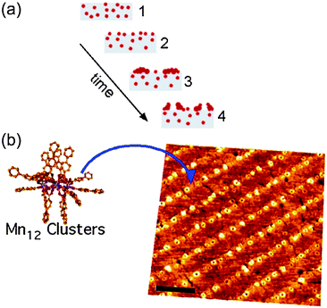
SMMs are the family of magnetic molecules most widely studied on surfaces. Since their discovery in the early 1990s,8 SMMs have been the focus of many investigations, motivated by the fact that these molecular exchange-coupled transition metal clusters show slow relaxation of the magnetization and magnetic hysteresis of purely molecular origin,4,41 thanks to the combination of large-spin ground states and high axial magnetic anisotropy.8,42 The first approach to deposit SMMs on surfaces was attempted by Coronado and co-workers.43,44 By making use of the Langmuir–Blodgett technique, the authors created a surfactant molecular film at the air–water interface where Mn12 clusters arrange both in the form of isolated molecules and/or well-defined monolayers, which may exhibit magnetic anisotropy depending on the orientation of the film with respect to the applied magnetic field. This fact was attributed to the preferential orientation of the complexes with their easy magnetization axis normal to the film surface. After this pioneering work, numerous experimental studies for the deposition and nanostructuration of SMMs on different surfaces have also been reported, mainly devoted to the archetypal SMM, the dodecamanganese acetate cluster (Mn12-ac) and its derivatives, because of their large anisotropy barrier and very-slow spin dynamics at low temperature. However, promising SMM families have recently emerged and attention is also addressed in organizing these molecules on a surface. In general, SMM like behaviour is described by: (i) large magnetic moment in the ground state, (ii) high magnetic anisotropy due to large zero-field splitting and (iii) slow relaxation of the magnetization.
Among this variety of magnetic molecular materials available on surfaces this review, which does not pretend to be exhaustive, will focus on SMMs, though other families such as metal phthalocyanines generally referred to also as Single Ion Magnets (SIM) or antiferromagnetic rings, also known as Molecular Spin Clusters (MSC) will also be included in some sections. Section 2 of this paper pretends to be an in-deep review of the advances on the structuration of different families of SMMs on surfaces and the deposition techniques used to this end.
On the other hand, the evolution from bulk to single molecules grafted on a surface encloses other fundamental aspects that need to be addressed in parallel. It is widely known that nanoscale dimensions favour the appearance of new phenomenologies different from the characteristic bulk features of the sample, that arise from the different role of intermolecular interaction forces and also with the environment.45,46 Surface effects as well as interaction with the substrate can completely change the characteristic SMM behaviour observed in crystals, either increasing its magnetic anisotropy or completely removing it. To assess the nanostructuration effect on the properties of molecular magnets, new characterization tools that fulfil the sensitivity and nanometric resolution requirements to study magnetic molecular complexes on surfaces are required. Two different trends following this aim have been followed.
In the first approach, typical magnetic characterization techniques for bulk crystalline samples such as Superconducting Quantum Interference Devices (SQUID magnetometer) or Hall sensors have been miniaturized to increase their sensitivity down to a single magnetic nanoparticle moment, though the single SMM moment limit has still not been reached. Moreover, there is the need for the development of specific deposition and nanostructuration techniques to integrate the magnetic materials into the nanosensors with the required control on positioning and quantity of material. In Section 3, we will review state of the art on the sensitivity of these nanodevices and the pioneering approaches so far followed for the integration of magnetic molecular materials on hybrid devices.
On the second approach, common surface characterization techniques with atomic resolution such as STM have been applied to detect and study magnetic moments of molecules on different surfaces. The main limitation at the moment for the use of STM comes from the need to use robust enough molecules and suitable deposition techniques to work in ultrahigh vacuum conditions. Other alternative surface magnetic characterization techniques commonly applied for the study of thin films such as Magnetic Circular Dichroism (MCD), X-ray MCD (XMCD), Magneto Optical Kerr Effect (MOKE), or magnetic resonant techniques like β-detected Nuclear Magnetic Resonance (β-NMR) have been exploited with enhanced sensitivities to study large distributions of molecular magnets grafted on surfaces. The use of these techniques has allowed obtaining molecular magnetic features and substrate effects as averages on monolayers over the entire sample surface. In Section 3, we will review the different characterization techniques used for the magnetic characterization of nanostructures on surfaces, putting emphasis on their advantages and restrictions for the characterization of SMMs on surfaces.
2. Structuration of SMMs on surfaces
2.1. Nanostructuration on surfaces from solution
The easiest way to assemble molecules on a surface is by the direct deposition of a solution droplet of the target molecule and the posterior solvent evaporation or by dipping the native surface on the solution, whereupon pristine molecules are physisorbed via weak non-covalent interactions such as hydrogen bonds, ionic interactions, van der Waals forces, and hydrophobic interactions (Scheme 1a). For instance, thin films of Mn12-ac on Si substrates were directly created by dipping the native substrate in a diluted solution containing the SMMs and immediately removed.47 This method, named dip and dry, can be improved with the use of SMMs bearing external groups to favour a better assembly of the SMMs onto the surface in a more stable manner, through van der Waals and/or π–π interactions. This strategy was followed by Ruiz-Molinaet al. to study the structure of the SMM clusters when physisorbed on Au(111) surfaces by Atomic Force Microscopy (AFM).48 With this aim, they made use of a Mn12 derivative bearing biphenyl groups that enhance adsorbate–surface interactions by weak non-covalent bonds on Au. The initially formed molecular layer covers homogenously the whole surface, whereas further growth takes place mostly in the form of molecular wires (or aggregates) and occasionally as molecular islands. Interestingly, the Mn12 core is preserved for all the cases although its aggregation state appears to influence significantly the rigidity of the molecular aggregates. Force volume imaging experiments have demonstrated that molecules in the second layer are stiffer, i.e. more rigid, than the molecules lying at the background layer (Fig. 1). This fact clearly reveals that the interplay of attractive and repulsive forces between molecules and the molecule–surface interaction modulate the mechanical properties of the Mn12 SMMs upon grafting. These results are very important to understand how surface-induced morphological deformations can modify the magnetic properties of these molecular systems on the translation from the macroscopic bulk crystals to a surface.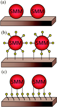 | ||
| Scheme 1 Representation of different strategies for the nanostructuration of SMMs on surfaces: (a) SMM direct deposition on a bare surface in order to immobilize the SMM via weak non-covalent interactions, (b) pre-functionalization of SMMs with functional groups able to interact chemically with the bare surface, (c) pre-functionalization of the surface with suitable functional groups able to interact with the SMM. | ||
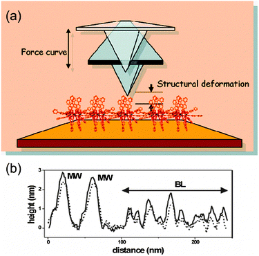 | ||
| Fig. 1 (a) Representation of the AFM experiments for the study of the differential surface effect on Mn12 directly in contact with the surface versus those separated by a molecular layer. The Mn12 SMMs bearing external biphenyl groups are deposited on Au(111) surfaces by the dip and dry method. (b) AFM surface profiles of a region exhibiting molecular wires (MW) and background layer (BL) Mn12 structures which demonstrate the influence of the SMM aggregation state on the stiffness of the structures. The scans were recorded sequentially at low (solid line) and high (dashed line) tip loads. Reprinted with permission from ref. 48. Copyright 2009 American Chemical Society. | ||
An alternative to the dip and dry method consists in the well-known drop casting approach. For instance, Bucher and co-workers simply deposited a very dilute drop on a Au(111) substrate (followed by solvent evaporation) to directly deposit the [Mn12O12(tBuCO2)16(H2O)4] or Mn12Piv16 SMM.49 Given that the direct deposition of Mn12Piv6 complexes from a solution is not a self-limiting process, they were able to grow several tens of monolayers at once by controlling the amount of solution added, which was useful to obtain a minimum quantity of material to perform SQUID magnetometer measurements. Later on, the drop casting method was also used by Ruiz-Molina and co-workers to study by STM the physisorption of the double-decker bis(phthalocyaninato) terbium(III) (TbPc2) on highly oriented pyrolytic graphite (HOPG).50 These studies revealed that the phthalocyanine molecules self-organize to form well-defined two dimensional assemblies with their molecular planes parallel to the graphite surface, i.e. with a preferential orientation of the magnetization axis perpendicular to the graphite surface. Due to their relevance for a full development of their magnetic characteristics as well as the development of possible future molecule-based devices, this issue has become a real challenge and will be discussed in Section 2.4.
Pre-functionalization of SMMs. This approach consists in the development of strategies to introduce specific functionalities around the magnetic core of the molecule that favour the binding of the clusters on native surfaces without altering the SMM behaviour (Scheme 1). The first attempts to graft functionalized SMM were inspired in the adsorption of organic thiol and sulfides on Au surfaces. For this, the acetate groups of the Mn12-ac were replaced by carboxylate groups containing thiol groups. This approach was applied for the first time by Cornia et al. to graft SMMs onto a Au(111) surface.51 They designed a 16-sulfanylhexadecanoate Mn12 derivative, in which thiol groups were acetyl-protected in order to avoid undesirable reactions in the presence of Mn12 centres. The deposition was carried out by incubating the Au substrate in a SMM solution in basic media to ensure the deprotection of thiol groups. The SMMs completely covered the surface with disordered layers, which could be disrupted by a continuous scanning of the area allowing the first imaging of well-isolated molecules of Mn12 on the surface by means of STM. Since then, several works reported new routes to organize Mn12 molecules onto surfaces exploiting the well-known ligand-exchange reaction.52–54 For instance, Cornia and Sessoli et al. reported a strategy based on the incorporation of thioether groups that also interact with Au, but in a weaker and more reversible way.53 The nanocluster was deposited by the incubation of the surface in a solution containing the Mn12 derivative. In this way, it was possible to obtain sub-monolayers (sML) of individually accessible clusters which could be imaged by STM. An extension of this study reported by the same authors investigated the influence of several experimental parameters, such as the solvent and the incubation time, on the molecular surface coverage.54
Besides the Mn12 family, other emerging SMM families have been pre-functionalized to be anchored on surfaces. The family of Mn6 SMMs, which contain six MnIII atoms, has received great attention due to the high effective energy barrier value of 86.4 K shown, together with an effective spin of S = 12. Two derivatives of Mn6, [MnIII6O2(sao)6(O2C-tp-3)2(EtOH)4] with spin ground state S = 4 and [MnIII6O2(Et-sao)6(O2C-tpc-3)2(EtOH)4(H2O)2] with S = 12, were anchored to Au surfaces through the use of 3-thiophenecarboxylate (tpc) ligands (Mn6-tpc) containing a S-atom. STM images revealed the formation of sML of isolated clusters with unaltered electronic structure after deposition as studied by X-ray Absorption Spectroscopy (XAS) and X-ray Photoelectron Spectroscopy (XPS).55,56
A different class of SMM comprising four high-spin Fe(III) ions, the Fe4 SMMs family, has been functionalized to promote interactions with different substrates. Fe4 SMMs functionalized with terminal alkenyl and thioacetyl groups57 were prepared by site-specific substitution on the complex [Fe4(OMe)6(dpm)6] (Hdpm = dipivaloylmethane) using derivatives of 2-(hydroxymethyl)propane-1,3-diol as incoming ligands, which can be sulfur functionalized to promote interactions with Au surfaces. The two tripods were located along the idealized threefold molecular axis, leading to wire-like molecular geometries that graft these molecules on H-terminated Si and Au substrates. The study of a monolayer of the resulting [Fe4(L)2(dpm)6] cluster (for which a ligand made up of long aliphatic chain was used to separate the molecule from the substrate) self-assembled on Au by means of XAS and XMCD demonstrated that the electronic structure and magnetic properties of this robust tailor-made Fe4 linked to Au were preserved upon grafting (Fig. 2).58,59Solvent effects on the resulting SMMs were also investigated by means of STM, XPS and Time of Flight Secondary-ion Mass Spectroscopy (ToF-SIMS).60 Finally, an alternative route to anchor the Fe4 cluster on Au through two 1,2-dithiolan-3-yl alligator clips has been reported.61
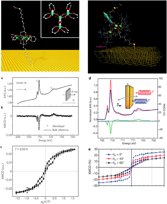 | ||
| Fig. 2 (top) Schematic representation of a Fe4 derivative bearing thiolate-terminated aliphatic long chains (left panel) and short chains (right panel) self-assembled on a Au surface. Inset left panel: magnetic core structure of Fe4, the arrows indicate the ground-state spin arrangement. (a, d) Iron L2,3-edge XAS spectra recorded using left-(σ+) and right-(σ−) hand circularly polarized light and H = 3 T on (a) the Fe4 monolayer with short aliphatic chains (T = 0.50 ± 0.05 K) and (d) on the Fe4 monolayer with long aliphatic chains (T = 0.65 ± 0.05 K)—left axis, blue and red lines. (b, d) XMCD spectrum obtained as (σ− − σ+) recorded in similar experimental conditions (b) on a thick film of Fe4 with long aliphatic chains on the same substrate and (d) a monolayer of Fe4 with short aliphatic chains (green line—right axis). (c) Magnetic hysteresis for the Fe4 monolayer with long aliphatic chains at T = 0, 50 K monitored through the XMCD intensity (multiplied by −1) at 709.2 eV obtained from XAS signals normalized to the pre-edge intensity (704.0 eV). The error bars represent the standard deviations estimated by averaging over three field cycles. A sweeping rate of 2 mT s−1 has been used. (e) Angle-resolved hysteresis loops for the Fe4 monolayer with short aliphatic chains obtained from the XMCD at 709.2 eV and T = 0.65 ± 0.05 K. Left panel: Reprinted by permission from Macmillan Publishers Ltd: Nature Materials ref. 58, Copyright 2009. Right panel: Reprinted by permission from Macmillan Publishers Ltd: Nature ref. 127, Copyright 2010. | ||
Cr7Ni molecular antiferromagnetic rings are a new class of molecular nanomagnets (MNM) that also show interesting quantum phenomena62 and have also been proposed as candidates for the implementation of quantum gates.63 Corradini et al. have obtained sML distributions of sulfur-functionalized derivatives on Au(111) surfaces, from the liquid phase.64 By using four different sulfur derivatives with a different number, location and orientation of the S groups,65 they were able to demonstrate that in all cases a robust grafting of the molecules on the Au substrate was obtained. The best results in terms of level of coverage and bonding robustness as well as smallest percentage of free ligands on the substrate was obtained for the Cr7Ni derivative functionalized with one peripheric 3-4-methylthiophenyl-propionate (MTPP) ligand (Cr7Ni-4mtpp), for which the binding to the substrate is done through a single protected S-atom. In contrast, functionalization with S-free derivatives yields smaller bonding strengths.
Functionalization of SMMs can be designed to favour the attachment to specific substrates, such as graphene. Graphene has recently been the focus of considerable interest due to its fascinating mechanical and electrical properties, and is a promising candidate for applications in electronics, as a one-atom-thick layer material to build ultrasensitive probes. Deposition of molecules on graphitic layers like carbon nanotubes (CNT) or graphene shows some limitations. The molecules need to be physisorbed on the carbon surface without the formation of covalent bonds that otherwise can strongly modify the structural and electronic properties of the substrate, and consequently alter the performance of graphene based devices. Instead, non-covalent π-stacking should preserve graphene intrinsic features while providing an effective coupling with the magnetic properties of molecules grafted on it. Most of the efforts to graft magnetic molecules on graphitic surfaces have been performed on CNT in perspectives for potential applications of CNT-based devices. A recompilation of such experiments will be reviewed in Section 3.2. Still, Lopes et al. have recently published a study of the interaction of SMMs grafted on graphene by combined AFM and Raman microspectroscopy. Pyrenyl-substituted heteroleptical TbPc2 (pyrene-TbPc2) were deposited on graphene by drop casting of a pyrene-TbPc2 solution, followed by rinses in dichloromethane and isopropanol to remove the residual sample.66 This decoration process is directly applicable in situ to graphene-based devices, i.e.graphene transistors. Pyrene groups and alkyl chains are well-known to exhibit an attractive interaction with the sp2carbon materials, thus resulting in the coupling of the pyrene-TbPc2 molecules with the graphenevia van der Waals interactions. Raman spectroscopy is used to confirm in a fast and non-destructive way that both TbPc2 and graphene electronic properties remain intact, and that only small charge transfer occurs.
Pre-functionalization of surfaces to chemically bind SMMs. Another experimental approach is based on the pre-functionalization of the surface allowing for the deposition of the SMM through strong covalent ligand-exchange reactions or electronic interaction (Scheme 1c). The strategy was exploited by Bucher and co-workers to covalently bind the Mn12Piv16 cluster to Au(111).49,67 Two different organosulfurs, 1,16-mercaptohexadecanoic acid and 11-mercaptoundecanoic acid, were used to functionalize the surface with terminal carboxylic groups accessible for the optimal attachment of the clustersvia ligand-exchange reaction. STM images of the resulting substrate revealed molecules of Mn12Piv16 arranged into domains of ordered monolayers. The partially ordered layer described in this work49 has been discussed by Voss and co-workers,68 who suggested that the results could be influenced by a multiple tip artefact. They investigated the topography and electronic structure of Mn12-parafluorobenzoate [Mn12O12(O2CC6H4F)16(H2O)4] or Mn12-pfb deposited via ligand exchange reaction on two differently pre-functionalized Au(III) surfaces with 4′-mercapto-octafluoro-biphenyl-4-carboxylic acid (4-MOBCA) and 4-(mercaptomethyl)-2,3,5,6-tetrafluorobenzoic acid (4-MMTBA). A partial ordering of the Mn12-pfb moieties on the 4-MMTBA seemed to be visible by STM, though the authors showed that it was simply an artefact due to the low conductivity of the Mn12-pfb/4-MMTBA system. These results showed similarities with the partial ordering of the Mn12-piv on the pre-functionalized surface with the 1,16-mercaptohexadecanoic acid reported by Bucher and co-workers.49 Voss and co-workers suggested the possibility that also in that case the conductivity of this system was also too low, which may also have resulted in an apparent ordering of the Mn12-piv moieties due to a STM tip artefact. On the other hand, they reported the possibility of influencing the assembly of monolayers of Mn12 SMM on a pre-functionalized Au (111) surface by using flexible linker molecules,68 which might allow the deposition of ordered Mn12 monolayers due to sterical reasons. However the low conductivity of these linker molecules reveals the need for a compromise between conductivity and flexibility of the functionalization layers used for the anchoring of Mn12.
Along this line, Burgert and co-workers made use of two types of short and highly conductive molecules for the modification of the Au surface: 4-MOBCA and 4-mercapto-2,3,5,6-tetrafluorobenzoic (4-MTBA).69 This approach ensured not only the effective grafting of the Mn12 clusters but also the optimal electronic coupling of the SMM with the surface necessary for the investigation of the electronic structure of the Mn12 cluster by means of scanning tunnelling spectroscopy (STS).70
In another interesting work, Voss et al. studied the direct grafting on an unmodified Au surface of the Mn12-thiophene-3-carboxylate (Mn12th) cluster, which contained thiol-modified ligands to promote strong S–Au interaction.71 A second strategy was the deposition of a Mn12-biphenyl-carboxylate (Mn12-biph) via ligand-exchange reaction on the Au surface, which was pre-functionalized with 4-MTBA. Both SMM monolayers were studied by means of STM, XPS, XAS and resonant photoelectron spectroscopy (RPES). The investigations on the SMM monolayer obtained by the direct deposition of the Mn12 derivative on native Au indicated a strong fragmentation of the Mn12 core. On the other side, the pre-functionalization of the surface was found to be optimal for the deposition of intact Mn12 clusters. These results are important to properly understand the influence of not only the surface but also of the grafting mechanisms on the SMMs properties.
Most of the work so far reviewed in this section has been focused on the deposition of Mn12 SMMs exclusively on pre-functionalized Au surfaces. Since this approach can be extended to many other surfaces covered with terminal carboxylate groups, this opens up the possibility to graft SMMs on surfaces with relevant technological importance such as Si (100).72–74Mn12 derivatives have been covalently grafted on Si surfaces pre-functionalized with carboxylate groupsvia thermal hydrosylation reaction between H-terminated Si(100) and methyl 10-undecenoate (Fig. 3a,b).72 After removal of the protecting ester groups, the surface was treated with a solution containing the Mn12-ac clusters to anchor the SMMs to the organic layer by means of ligand-exchange reaction. Furthermore, the possibility to control the density of the Mn12 clusters grafted on the Si(100) was investigated by tailoring the presence of carboxylate receptors on the surface using a mixture of methyl 10-undecenoate and 1-decene as an unreactive spacer.74
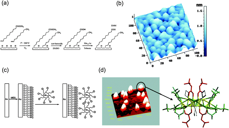 | ||
| Fig. 3 (a) Three-step procedure for anchoring of Mn12 on Si(100) pre-functionalized with carboxylic acids with control on density of SMM grafted by tuning the presence of the carboxylate receptors on the surface using unreactive spacers and (b) 3D AFM image of the SAM after the anchoring of Mn12. (c) Schematic procedure to immobilize via electrostatic interactions a polycationic Mn12 molecule on a Au surface previously modified with anionic self-assembled monolayers and (d) STM analysis of the SMMs once grafted on the surface. Reprinted with permission from ref. 74 and 75 (panels (a, b) and (c, d), respectively). Copyright 2006 Wiley-VCH Verlag GmbH & Co. KGaA and 2005 American Chemical Society. | ||
Finally, a variant that combines both the chemical modification of the surface and of the Mn12 clusters through electrostatic interactions as the driving force has also been described. Such ionic approach, proposed by Coronado et al., led to individually accessible Mn12 clusters grafted on Au (Fig. 3c,d).75 The approach involved the pre-modification of the Au with sodium mercaptoethanesulfonate HS(CH2)2SO3Na (MES) in order to functionalize the surface with negatively charged SO3− terminated groups. Then, the chemically modified surface was immersed into a solution containing a polycationic Mn12 derivative, which contained the 16 quaternary ammonium substituent in its periphery (Mn12-betaine). For short incubation times of the surface in the SMM solution, a partial coverage of well-isolated molecules on the surface takes place while the formation of 3D aggregates for longer incubation times is observed. Even more, the maximization of the number of ionic interactions between the cationic ligands and the negatively charged organic layer seemed to induce a preferential orientation of the Mn12-betaine molecules with their magnetic axis perpendicular to the surface, as suggested by STM analysis.
In a similar procedure, Ghirri et al. have recently shown the deposition of Cr7Ni molecular rings on graphite from the liquid phase.76 They elaborated a route involving the preparation of a buffer layer with pure electrostatic interaction with the substrate, which can also help to stabilize the molecules through ionic interactions between the buffer and the sample. More specifically, they used a self-assembled monolayer (SAM) of alkane sulfonates deposited on HOPG and then suitable cationic clusters of different Cr7Ni derivatives were immobilized on the anionic SAM.
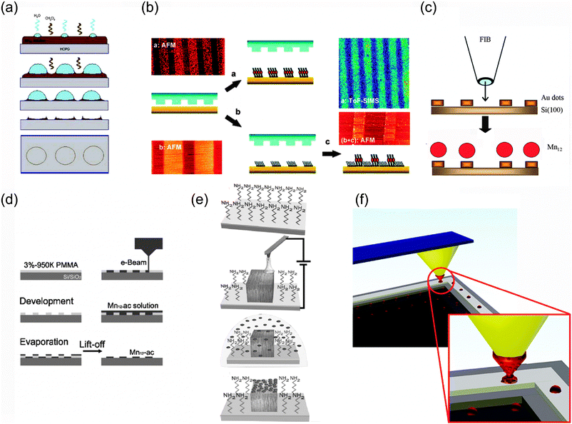 | ||
| Scheme 2 Patterning strategies used for the fabrication of SMM-based arrays on the surface. Schematic representation of the techniques: (a) breath-figures templates (b) microcontact printing (μCP); (c) focused ion beam (FIB) lithography; (d) electron beam lithography (EBL); (e) local oxidation nanolithography (LON) and (f) dip pen nanolithography (DPN). Reprinted by permission from ref. 77, 79, 86 and 87 (panels (a), (b), (d) and (e), respectively). Copyright 2005 The Royal Society of Chemistry, 2005 American Chemical Society, 2007 American Institute of Physics and 2007 Wiley-VCH Verlag GmbH & Co. KGaA, respectively. | ||
Breath-figure templates. Ruiz-Molina and co-workers have reported a procedure for obtaining self-assembled molecular magnetic rings, taking advantage of the breath figures phenomenon (Scheme 2a).77 Specifically, water droplets formed upon cooling evaporation of the solvent were used as templates to arrange Mn12 bearing aromatic biphenyl groups by non-covalent interaction with the surface. The same breath figures phenomenon made possible the fabrication of highly ordered honeycomb structures by drop casting a solution of a Mn12 modified with stearic acid (CH3(CH2)16COOH), the Mn12O12(C17H35COO)11(CH3COO)5·H2O (Mn12-st) on glass and mica substrates at high relative humidity.78 By changing the concentration of the Mn12th cluster solution, 2D and 3D honeycomb structures were successfully obtained.
Stamp-assisted (soft-lithography) techniques. This method consists in covalent grafting of SMMs by applying direct and indirect variations of the microcontact printing technique (μCP). This strategy has afforded ordered Mn12 sulfur-derivative monolayer stripes with widths of 5 μm onto Au (Scheme 2b).79 However, in all these cases, the SMM structures obtained were far from the nanoscale range. Attempts to organize such molecules into ordered structures at the nanometre scale have made use of unconventional lithographic techniques.80–82 For instance, a stamp-assisted deposition technique called lithographically controlled wetting (LCW) has been used for the nanostructuration of Mn12 clusters by the confinement of a solution containing the molecules to the protruding regions of a stamp placed on top of the solution layer.80
Lithography assisted structuration. The standard photolithographic approach is a straightforward way to fabricate micron-sized patterned Mn12 films into arbitrary shapes on Si/SiO2.83 More recently, other methods have been implemented, which are mainly indirect procedures where pre-patterned surfaces are firstly fabricated to confine the SMM deposition to pre-determined nanoscale regions of the surface. The techniques used are (i) focused ion beam (FIB) lithography, (ii) electron-beam lithography (EBL) and (iii) local oxidation nanolithography (LON). High-resolution FIB milling was used to pattern matrices made of 100 × 100 nm2Au dots, on which sulfur-functionalized Mn12 derivatives were adsorbed in the sML coverage range (Scheme 2c).84 The authors made use of Mn12 bearing anthracene-1,8-dicarboxylate ligands (Mn12-adc), which are expected to favour a preferential orientation of the clusters with the easy axis perpendicular to the surface.85 Teizer and co-workers demonstrated the capabilities of EBL (Scheme 2d) for the formation of high-resolution nanopatterns of Mn12-ac with arbitrary shapes, such as lines with a reduced width of only ∼50 nm,86 after confirming that the lithographic chemicals used in this study do not interfere with the core properties of Mn12. The LON technique exhibits excellent resolutions and permits the fabrication of dots and stripes of only few nanometres, which can be used as templates for the selective deposition of Mn12 clusters. Coronado and co-workers took advantage of the combination of this top-down nanolithography technique with electrostatic interactions for the SMM patterning.75 They fabricated silicon oxide templates on a Si(100) surface by means of LON to induce a preferential interaction between positively charged Mn12 clusters and the local oxide nanopatterns (Scheme 2e).87 Prior to the local oxidation, the Si(100) surface was modified with an amino-terminated monolayer to induce a repulsive interaction between the positively charged SMM and the rest of the non-oxidized surface. More recently, LON has been used to fabricate 1D arrays of individual ferritin molecules (Fig. 4).88 Selective deposition was driven again by the electrostatic interactions existing between the protein and the silicon oxide templates. The use of electrostatic interactions presents an extra advantage: on top of giving control on the positioning, they also allow to switch the interaction, that is, to have control on the attachment/removal of this molecule on the surface by changing the pH of the solution media as demonstrated by the authors. This approach could be successfully generalized and extended in order to pattern ferritin particles over macroscopic regions by making use of print-based methods such as lithography-controlled dewetting instead of LON.
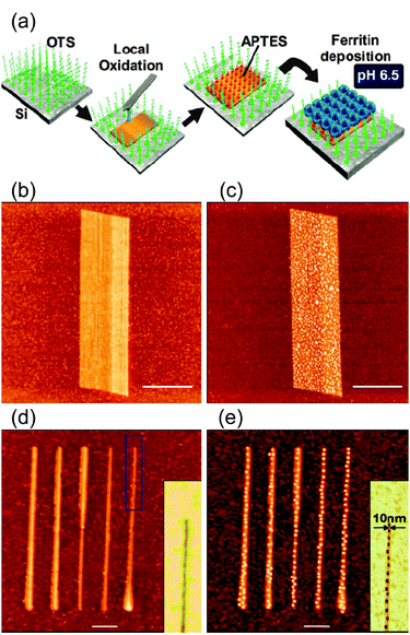 | ||
| Fig. 4 (a) Schematic representation of the site-selective deposition of ferritin molecules onto silicon oxide templates fabricated on a Si(100) by means of local oxidation nanolithography (LON). AFM image of an oxide pattern (b) before and (c) after ferritin deposition process. (d) Parallel array of oxide lines whose widths accurately match the protein size (10–15 nm). (e) Same array after the deposition of ferritin molecules, which arrange into chain-like structures giving to 1D arrays. The insets of (d) and (e) show the AFM phase image of a section of the corresponding topography AFM image. The scale bars are 1 μm in (b,c) and 100 nm in (d,e). Reprinted with permission from ref. 88. Copyright 2010 Wiley-VCH Verlag GmbH & Co. KGaA. | ||
Dip-pen nanolithography . DPN has already shown its enormous potential for structuring a wide diversity of substances on surfaces with high resolution (Scheme 2f).89–91DPN allows the control on the nanostructure shape and size in a wide range of substrates of technological interest, such as Au, Si and Nb. Maspoch and co-workers have recently developed a direct route for the nanopatterning of ferritin particles by direct-write DPN without the need for any previous functionalization of the substrate nor the molecule, or the application of external stimuli.92 Even more interesting is the fact that ferritin molecules deposited on each dot organized as sML, as observed by AFM. In addition, DPN enables a fine control on the number of particles deposited onto a surface (Fig. 5).93 The same authors demonstrated that the number of ferritin particles deposited on a dot-like feature can be controlled by knowing the contact angle between the ink protein solution and the substrate, and by selecting the initial protein concentration and the dot-like feature diameter.
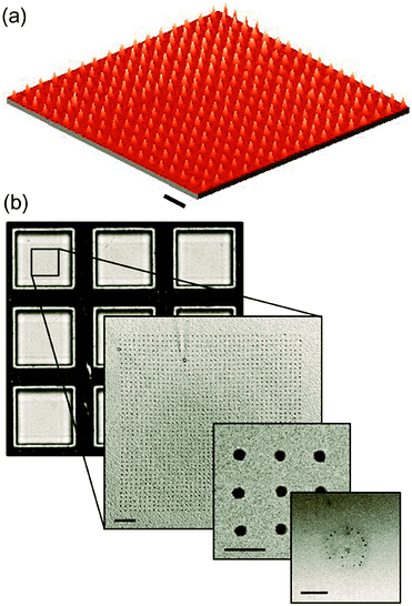 | ||
| Fig. 5 (a) 3D AFM image of a ferritin array with dot diameters of 100 nm fabricated on Au by means of direct-write dip pen nanolithography (DPN). (b) TEM images of a ferritin nanoarray with dot diameters of 150 nm generated by direct-write DPN on a TEM grid. The central inorganic core of the protein allows its visualization by TEM, and therefore, the study of the number of ferritin molecules deposited on each dot. The scale bars are 1 μm in (a) and 2 μm, 500 nm and 100 nm for the different magnifications in (b). Panel (a): see ref. 92. Panel (b): reprinted with permission from ref. 93. Copyright 2010 Wiley-VCH Verlag GmbH & Co. KGaA. | ||
Other examples of assembly of molecular magnets on CNT are reported by Charron et al.,103,104 who showed the first direct assembly of a SMM polyoxometalate (POM) of formula [Fe4(H2O)2(FeW9O34)2] (Fe6POM) on a CNT with preservation of the SMM behaviour upon assembly. This finding was consistent with the hypothesis that the tungsten oxide matrix chelating the Fe4 moiety prevents extensive deformation of the coordination sphere of the magnetic ions and thus precludes a dramatic change in the anisotropy behaviour when the molecules are not assembled within the crystal. The same research group extended the grafting of the paramagnetic POM of formula [As2W20O68Co(H2O)] (CoPOM) together with its isostructural diamagnetic analogue [As2W20O68Zn(H2O)] (ZnPOM). The functionalization in all cases is done by simply stirring of single-walled CNTs in presence of polyoxometalate molecules. Therefore, the use of magnetic ions encapsulated in polyoxometalate matrices holds great promise for the design of robust spintronic devices based on CNTs and magnetic molecules.
Apart from the control on grafting without introducing local defects, it is also of crucial importance to demonstrate that at least the SMMs retain their structural integrity and magnetic identity when grafted on the CNTs. With this aim, another example of a magnetic molecule with SMM like behaviour, the heteroleptic TbPc2, bearing a pyrenyl group, was successfully attached onto a SWCNT with π–π interactions,105 by immersing the CNT in a solution of the SMM. The supramolecular assembly was obtained via π-stacking interactions between the pyrenyl groups and the CNT walls and shows even improved magnetic anisotropy, probably due to the suppression of intermolecular interactions. Survival of the SMM behaviour of the conjugate was proved by bulk ac-magnetic susceptibility measurements on a SQUID magnetometer.
2.2. Physical techniques for SMM deposition on surfaces
All the approaches described in Section 2.1 are solution-based techniques that are not suitable to be used in combination with in situ ultra-high vacuum (UHV) characterization techniques. Instead, physical techniques such as pulsed laser deposition (PLD)106 and matrix assisted pulsed laser evaporation (MAPLE)107,108 can be used. The main limitation for using these techniques is the thermal stability of the SMM that can be overcome either by using low energy processes that prevent the cluster fragmentation or by the use of robust SMM clusters. Sessoli and co-workers demonstrated that it is possible to mould a derivative of the Fe4 cluster, the [Fe4(Ph-C(CH2O)3)2(dpm)6] or Fe4-Ph, into variable-thickness films by thermal evaporation under high-vacuum conditions without inducing changes in the chemical structure or in the magnetic properties of the cluster due to its robustness and resistance to prolonged heating and HV conditions.109An alternative deposition route, able to fabricate films of intact Mn12 under controlled vacuum conditions on different surfaces, is the direct injection of a spray containing a solution of the SMM.110 The vacuum spray technique allows not only the deposition of unaltered SMM but also the control on the thickness of the fabricated films from μm down to the nm range. Even though there is no preferential orientation of the Mn12-ac molecules deposited on the surface, the roughness of the films with thickness under 150 nm is really low, of the order of 4 nm. Moroni et al. deposited Mn12-ac by vacuum spray on transparent LiF substrates and demonstrated the preservation of its SMM behaviour by MCD measurements.110 Saywell and co-workers made use of the non-thermal technique of the electrospray deposition process in UHV (UHV-ESD) for the deposition of Mn12-ac and [Mn12O12(O2C6H5)16(H2O)4] or Mn12-bz clusters on a Au surface.111,112 They observed that the SMMs self-assembled in low-dimensional molecular chains as a result of the anisotropic nature of the molecule–molecule and molecule–substrate interactions. Successful attempts to deposit SMMs under UHV conditions have been carried out for other SMMs based on lanthanide bis-phthalocyaninato (LnPc2)113,114 such as TbPc2 SMMs complexes.114 Vitali and co-workers investigated the electronic structure of TbPc2 on a Cu(111) surface by STM, DFT and STS. The authors deposited the SMM under UHV conditions using a method named dry imprinting114 that makes use of a soft applicator formed by a fibber-glass bundle coated with a fine-grained powder of the SMM crystals; the clusters are directly deposited on the Cu(111) surface when the coated bundle is brought into gentle contact with the surface (Fig. 6). Simultaneously, Stepanow et al. have reported the magnetic properties of isolated TbPc2 molecules supported on a Cu(100) surface deposited by thermal evaporation.115 In fact, a recent review appeared while writing this paper that compiles several examples of self-assembled nanometre-scale magnetic networks deposited under vacuum conditions.116
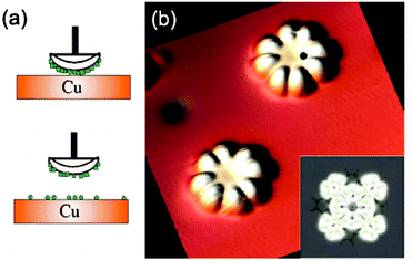 | ||
| Fig. 6 (a) Schematic representation of the deposition of TbPc2 on Cu(111) in UHV by means of a dry imprinting technique. (b) Constant current topograph of two isolated TbPc2 molecules supported by the Cu(111) surface (image size, 7 nm × 7 nm; tunnelling conditions, −0.8 eV, 0.7 nA). The inset shows simulated STM image of an isolated TbPc2 molecule. STM measured energy resolved conductance maps of this molecule are shown in Fig. 28. Reprinted with permission from ref. 114. Copyright 2008 American Chemical Society. | ||
2.3. Polymer assisted structuration on thin films
The incorporation of the SMMs on a thin film or host material suitable to be processed while keeping their chemical integrity and magnetic identity has faced the following different perspectives. Steps towards this goal are the incorporation into matrices such as mesoporous silica,117 organic polymers such as poly(methyl methacrylate) (PMMA) or polycarbonate (PC),118 the formation of hybrid polymers by the polymerization of magnetic clusters in the presence of organic monomers,119 and the use of CNTs, exfoliated graphite and diatoms for the encapsulation of SMMs.120,121 However, these examples are far from the scope of this review, which is more focussed on the deposition of thin films of magnetic molecules on surfaces.We will do review those specific examples where SMMs have been incorporated and brought to the surface of a thin film.122,123 A simple and reliable methodology to address individual SMMs on a thin film surface was initially explored by Veciana and co-workers.81,82,124 A polymeric thin film made from a polycarbonate matrix and the [Mn12O12(O2CC12H9)16(H2O)4] complex was treated with different vapour organic solvents that induced the emergence of a small fraction of clusters on the surface of the film. The aggregation state of the Mn12 molecules onto the film surface can be controlled depending on the nature of the organic solvent. The authors subsequently reported another approach that combines the demixing process of a binary polymer/Mn12 mixture with soft-lithography (Fig. 7).82 In this way, following a stamp-assisted deposition with a DVD as a structured master, they obtained a replica made of a mixture of the Mn12 clusters and the polymer. When the film is exposed to a saturated atmosphere of solvent vapour, the replica experiences a smoothening of its topography and the Mn12 molecules concentrated preferentially in the regions corresponding to the original protrusions. Following this approach, magnetic patterns of Mn12 that closely reproduced the topographic indentations of the DVD master were obtained and imaged by means of Magnetic Force Microscopy (MFM).82 An extension of this work was developed later on by the same authors reporting the capabilities of this patterning process for ordering nanosized rings of SMM into parallel lines of nanometric width.81
 | ||
| Fig. 7 (a) Schematic illustration of the patterning process for fabricated nanosized rings of Mn12 molecules ordered into parallel lines by combining the demixing process of a binary polymer/SMM mixture with soft-lithography (step 1, film as prepared; step 2, demixing; step 3, droplet formation; step 4, nanoring formation). (b) AFM image of the nanoring formation. The scale bar is 1 μm. Reprinted with permission from ref. 81. Copyright 2006 American Chemical Society. | ||
Another development came from Coronado and co-workers, who managed to embed a [Mn12O12(H2O)4·(C6F5COO)16] or Mn12-PhFs into conducting polymers.125,126 The incorporated Mn12 molecules oxidized the arylamine polymer resulting in a hybrid material with increased conductivities. This partially oxidized composite remained completely soluble, thus allowing for its easy processing into thin films by spin-coating from solution. Homogeneous and transparent films with thickness between 20 nm and 200 nm were obtained with this procedure. The resulting high conductivity of this material, which reached values of ∼0.01 S cm−1, makes it suitable as charge-transport material in organic cells and organic light-emitting diodes (OLEDs).
2.4. Orientation of SMM in self-assembled monolayers
Up to this point, different physical and chemical approaches used for the structuration of SMMs on surfaces have been described. The variety of alternatives is notably large, especially considering the relative novelty of the field. Such enormous diversity of techniques allows nanostructuration of SMM on surfaces where morphology, number of layers and nature of the SMM can be systematically tuned. However, along with the controlled grafting on surfaces, another important challenge that scientists are facing and that needs to be addressed is the orientation of the molecules on the substrate. Magnetic properties of SMMs are based on easy-axis anisotropy that induces a preferential orientation of the magnetization in a certain direction. Thus, it is critical to control the direction of the easy magnetization axis of these molecules in views of exploitation of its characteristic magnetic features, such as quantum tunnelling effects.127Pioneer work to orient the easy magnetization axis of the clusters on the surface was done by Coronado et al., who obtained a Mn12 film with the Langmuir–Blodget technique that exhibits magnetic anisotropy.43,44 Later on, Ruiz-Molina and co-workers deposited a double decker that self-organizes on a surface with its molecular planes parallel to the surface, i.e. with the magnetization axis perpendicular to the surface.50 Further attempts to orient SMMs consisted in the partial functionalization of the SMMs by ligand substitution with binding surface groups that introduce chemical anisotropy to the molecule and orientational restrains to its binding with respect to the surface.85,127–130 For instance, Christou and co-workers prepared mixed-carboxylate complexes selectively ordered on axial and equatorial positions due to the preference of different carboxylates to occupy specific sites on the molecule.128 This has been rationalized on the basis of the relative basicities of the carboxylate groups. Some other interesting approaches have specifically designed chlorine marked mixed-ligands SMMs to monitor the ligand-exchange reaction by XPS and determine whether the nanoclusters are successfully oriented when grafted on surfaces or not. This strategy was used by Mallah and co-workers, who demonstrated the preferential orientation of Mn12 molecules with their anisotropy axes parallel to the Si surface.131,132 For this study two types of Mn12 derivatives were used (Fig. 8a): (i) a Mn12 derivative with dichloroacetate groups in both axial and equatorial positions and (ii) a mixed Mn12 derivative functionalized with dichloroacetate groups in axial positions and tert-butyl acetate groups in equatorial positions. The clusters were grafted by immersion of a carboxylic acid-functionalized Si(100) surface in a solution containing the SMMs. The ligand exchange reaction was driven by the formation of the most thermodynamically stable Mn12, where the most basic carboxylate ligands are located on the equatorial positions while the less basic ones occupy the axial positions (Fig 8b). In both cases, XPS revealed the selective exchanging of all the equatorial carboxylates by the carboxylic groups from the functionalized Si(100) surface.
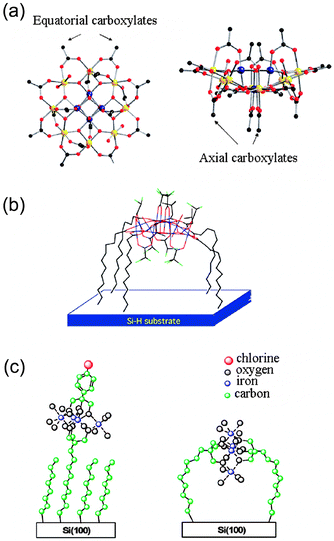 | ||
| Fig. 8 (a) Molecular structure of Mn12, whose axial and equatorial carboxylate groups are indicated. (b) Proposed model for the assembly of Mn12 whose equatorial carboxylates have been selectively exchanged with the carboxylic groups from the pre-functionalized Si(100) surface. (c) Possible orientation of Fe4 SMM linked through one or two surface-bound tripods of pre-functionalized Si surfaces with tripodal receptors. Panels (a) and (b): reprinted with permission from ref. 132. Copyright 2009 The Royal Society of Chemistry. Panel (c): reprinted with permission from ref. 134. Copyright 2008 American Chemical Society. | ||
Fonin and co-workers have shown the influence of the ligand shell of Mn12 clusters on their orientation when deposited via ligand exchange reaction on Au.133 They investigated the grafting of a Mn12-diphenylphosphinate derivative on the Au surface which was pre-functionalized with 4-MOBCA by means of STM and STS. The measured high profiles suggested a random orientation of the moieties on the surface, and such a result could be explained due to the equal high acidity of the diphenylphosphinic acid and of 4-MOBCA. Contrary to that, a preferential orientation with the easy axis perpendicular to the surface was obtained when grafting a Mn12th. In this case, the cluster orientation was attributed to the higher acidity of 4-MOBCA compared to thiophenecarboxylate ligands, which favours the ligand substitution only at the axial positions. A different route for the site-specific functionalization of Mn12 clusters was proposed by Sessoli and co-workers.85 They demonstrated that the selective Mn12 functionalization can be favoured by the entropy gain from chelate ring formation, thus providing an efficient route to greatly improve the selectivity of the ligand substitution by using dicarboxylate ligands such as anthracene-1,8-dicarboxylic acid, which leads to a selective occupation of axial binding sites. These results suggest the use of pre-modified surfaces with anthracene-1,8-dicarboxylates for the controlled deposition of Mn12 moieties with their easy axes perpendicularly oriented to the surface.
Other families of SMMs have also been grafted with a preferential orientation of their easy axis with respect to the surfaces. In a subsequent work, Sessoli and co-workers suggested the use of the site-specific binding properties of the trimethylol function toward the Fe4 SMM for grafting these moieties on H-terminated silicon surfaces (Fig. 8c).57 The grafting route was investigated by the pre-functionalization of a Si surface with tripodal receptors derived from 2,2-bis(hydrocymethyl)-10-undecen-1-ol.134 The modified surface was reacted with two types of Fe4 clusters, the [Fe4(OMe)6(tmhd)6] and a chlorine-marked complex [Fe4(L)2(tmhd)6] (Htmhd = 2,2,6,6-tetramethylheptane-3,5-dione, H3L = 2-(4-chloro-phenyl)-2-hydroxymethyl-propane-1,3-diol), and investigated by means of XPS, attenuated total reflection-infrared spectroscopy (ATR-IR) and AFM. The results showed that the aggregation state and orientation of the grafted nanoclusters could be controlled by the density of the tripodal receptors present on the surface. For low receptor concentrations, the SMM clusters were linked to the surface through one receptor. In contrast, for higher receptor concentrations, the grafting of the clusters might occur through two surface-bound tripods. A more recent work explored a simpler and faster route for the direct grafting of the Fe4 SMM on Si by a one-pot procedure based on photoinduced hydrosilylation followed by an in situ ligand exchange reaction.135 The preferential orientation of the Fe4 complexes has also been feasible on Au.127 The cluster specially designed for grafting on Au wear a linker made of a short aliphatic chain containing five carbon atoms instead of the nine carbon atoms previously reported,58 and terminated by a sulfur-containing moiety (whose complete formula was [Fe4(L)2(dpm)6], where H3L is 7-(acetylthio)-2,2-bis(hydroxymethyl)heptan-1-ol). The use of longer aliphatic chains leads to the random orientation of the cluster, due to the binding of one or both ligands to the surface.60 By contrast, the use of this shorter linker of only five carbon atoms would prevent the grafting of both ligands to the surface, due to the steric hindrance of the Fe4 discoid. X-Ray natural linear dichroism (XNLD) measurements suggested the preferential orientation of the clusters with their easy axis close to the surface normal, what was further confirmed by means of periodic DFT calculations.
3. Integration into hybrid devices
The structuration of magnetic molecular materials on surfaces described in Section 2 has been essentially promoted in views of applications in different technological fields, for which it is required to have the molecules not only isolated on surfaces but also integrated into devices that allow their reading and manipulation. The goal is twofold. First, from a scientific point of view the objective is to study and understand the magnetization relaxation at the individual molecular level, and to see how these properties are affected on moving from the macroscopic (crystals or powder) to the nanoscopic (surfaces) world. It is clear that surface deposition will affect such properties. For instance, as reviewed in the previous sections, the strong interaction of the molecule with the substrate can modify the molecular geometry, and hence alter the easy magnetization axis of the molecule by comparison with that observed in a macroscopic crystalline environment. The second objective is to convert nowadays prospective ideas into future real market devices, where each molecule could be used as a bit of magnetic information or qubit for quantum computing, among other possible applications.Most of the hybrid devices that include magnetic molecular materials are directed to the detection of the magnetic moment of isolated magnetic molecules. In this regard, the most sensitive magnetic flux detectors are SQUIDs. Their development has been focused on the increase of their sensitivity to allow the detection of a single atomic spin,136,137 following two trends: the miniaturization of the devices and the maximization of the coupling factor between the device and the sample. Other hybrid devices include those dealing with transport properties through the magnetic molecular materials, such as single molecule transistors, or field-effect transistor (FET) devices of different natures. Integration of magnetic molecules into these devices requires structuration techniques that allow the deposition of very few molecules on nanometric targets with high accuracy.
In this section we will review the different approaches followed to integrate magnetic molecules on different sensors, as well as the magnetic and transport measurements that can be derived from them. Reports will include in some cases the integration and study of magnetic nanoparticles. Indeed, even this review is focused on SMMs on surfaces, we believe that it is well-grounded to include examples of hybrid nanodevices based on magnetic nanoparticles since they are at the state of the art of the evolution and magnetic sensitivity of these devices and the integration techniques shown here could be extrapolated to SMMs when the devices achieve the required sensitivity limit to detect isolated SMMs.
3.1. Hybrid SQUID devices
The development of SQUIDs has been closely tight to the aim of measuring the magnetization reversal of an individual magnetic particle or molecule.137 For this, two requirements must be fulfilled: first, SQUIDs have to increase their sensitivity up to a single molecule level, and second, single magnetic particles or molecules must be integrated on the areas of the device that show highest sensitivity.The magnetic flux variation ΔΦ detected by a SQUID is related to the magnetization ΔM change associated with the reversal of the magnetic moments: ΔΦ = αΔM, where α is the flux coupling factor, which is defined by the geometry of the sample and by the location of the sample on the device. The flux sensitivity for a SQUID is limited by the quantum limit. Experimentally, the poor flux coupling factor that the geometry of SQUIDs with this high sensitivity present limits the spin sensitivity up to 100–1000 spins, and prevents its use to detect the magnetization reversal of single spin magnetic moment. So it is not only necessary to have a sample with enough magnetic moment, but also to place it in the right position on the sensor to maximize the flux coupling factor.
Different geometries have been investigated to maximize the coupling factor of the material with the device. One of them is the use of the SQUID junction itself to detect the signal, i.e. by placing the spins directly onto the junction.142 This approach was used by Jamet et al. that performed the first measurements of the magnetization reversal on single magnetic nanoparticles with a new microSQUID set-up.143 Single 1000 atom cobalt clusters of about 3 nm diameter were directly embedded into the Nb junctions of a microSQUID. In this way, the coupling factor was highly improved, and they were able to detect the magnetization reversal corresponding to 103μBHz−0.5 by performing three dimensional switching field measurements of single magnetic Co nanoparticles.
The simplest method initially used to integrate the magnetic materials on the devices consists in a random deposition of the sample onto an array of sensors. This deposition is done either by drop casting, placing a drop of a dispersed solution of target particles on a chip containing some hundreds of devices,144 or by spray pyrolysis of nanodroplets of a solution containing the sample nanoparticles.145 After drying, the particles are physisorbed onto the chip, but only the ones falling in the sensitive zones of the sensors such as the nanobridge of the SQUID loop have enough flux coupling with the sensor to be detected. Those are selected for the magnetic measurements. In all these cases, the position and morphology of the particles is determined by Scanning Electron Microscopy (SEM) only after magnetization measurements are done. This procedure was used by Wernsdorfer and co-workers for the successful integration of individual nanosized nickel wires as well as magnetic nanoparticles of different types and sizes in the range of 10 nm to 50 nm onto microSQUID detectors.144,146,147 The major drawback of this methodology relies on the implicit poor control on the exact particle position.
Maximization of flux coupling. The challenge of integrating a controlled number of particles onto magnetic sensor devices such as microSQUIDs with accuracy and high flux coupling factor has been addressed by means of several strategies. It is important to emphasize that all the examples reported in this direction used magnetic nanoparticles while the measurement of molecular magnetic materials remains elusive. To the best of our knowledge, the closest approximation to a molecular material is the case of ferritin,148 which consists of a cage-shaped protein that naturally accommodates an inorganic nanoparticle of hydrated iron(III) oxide (we are not considering the measurement of molecular materials by depositing powders or microcrystals, but only those cases where there is a specific structuration on surfaces). This can be explained since the real sensitivity of micro or nanoSQUIDs is still far from the single molecule level and most of the times, material with high enough magnetic moment to be detected is needed.
To improve the control on the deposition, it is well known that the tip of the scanning probe microscopes (SPM) can be used as a tool for the accurate positioning of single molecules and clusters along smooth surfaces.149–153 In this sense, it has been demonstrated that DPN is an excellent technique to deposit a controlled number of magnetic nanoparticles as sML on the most sensitive areas of a microSQUID maximizing the magnetic flux coupling of the sample with the sensor (Fig. 9).148 As theoretically calculated, the highest coupling factor was located in the closest points to the wire corners of the microSQUID, and DPN allowed creating ferritin nanostructures accurately onto these regions, with fine control on the number of ferritins deposited on each feature.92,93 The precision reached with this integration process was also demonstrated by SEM images, and the maximization of the flux coupling was proved with the magnetic measurements performed with the hybrid sensor. Furthermore, it was demonstrated that the single monolayer arrangement of magnetic ferritin nanoparticles allowed a better thermalization of the sample with respect to traditional bulk measurements.148
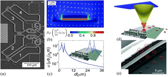 | ||
| Fig. 9 (a) SEM image of a microSQUID sensor with rectangular shaped pick-up coils with effective areas of 63 μm × 250 μm. (b) Finite element calculation of the excitation created by a primary coil when using a drive current of ip = 500 μA. (c) Numerical calculation of the coupling factor as a function of the distance from the center of the coil. The inset shows a 3D cross section of the pick-up and primary coil wires. (d) Schematic representation of the ferritin deposition process by DPN on the most sensitive areas of the microSQUID. (e) SEM images of the sensor right after the deposition of three rows of CoO@apoferritin dots. Reprinted with permission from ref. 148. Copyright 2010 American Institute of Physics. | ||
The first fully nanosized SQUIDs were reported by Lam and Tilbrook.157 They designed and fabricated a nanoSQUID with a hole size of 200 nm × 200 nm and shunted Nb nanojunctions, with a calculated sensitivity of 250 spins Hz−0.5 at 4.2 K. Actually, one of these devices operating in open-loop current biased mode was used to perform the first measurement of the magnetization reversal of a single ferritin. Vohralik and Lam detected the magnetization reversal of native horse spleen ferritin nanoparticles with a magnetic moment of μ < 300 μB.158 In this case, in order to optimize the flux coupling, they attached a small number of these organic nanoparticles directly over the nanojunction with a method combining monolayer self-assembling with electron beam lithography (Fig. 10).159 First a 200 nm × 200 nm window in the PMMA resistor deposited onto the gold over a layer of the Nb nanoSQUID is opened directly over the nanojunction by EBL. Then, in the second step, organic linker molecules are deposited directly over the exposed part of the gold and used to attach the ferritin magnetic molecules to the Nb nanoSQUIDs device.
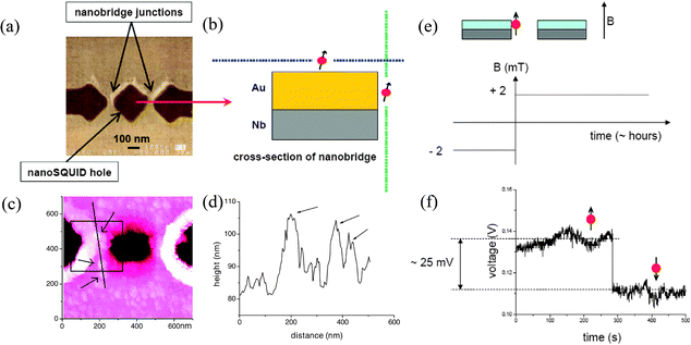 | ||
| Fig. 10 (a) SEM image of the nanoSQUID hole with two nanobridged junctions. (b) Idealized schematic cross section of one of the nanobridge junctions, showing the ferritin attached on top of the gold overlayer or on the sides of the gold layer. (c) AFM of a nanoSQUID with a scan area of 700 nm × 700 nm. Arrows indicate the positions of the ferritins and the square shows the approximate location of the PMMA window used for attachment. (d) Topography data for a line scan across the three ferritin particles indicated by arrows in (c). (e) Schematic showing the main features of the device for the measurement, having attached ferritin to the nanoSQUID. The sample was cooled down to 4.2 K in zero field and then the applied field was adjusted to the desired value and the bias current was optimized. (f) Keeping the field constant, the SQUID output voltage was recorded for a number of hours. In addition to slow drifts in the signal and a fairly constant level noise, larger jumps were also observed. These jumps may be the result of reversals of the magnetic moments of attached ferritin nanoparticles (as illustrated in the diagram). After recording the SQUID output for a number of hours, the applied field was changed and another measurement cycle was started. Reprinted with permission from ref. 158 and 159 (panels (a, b), (e, f) and (c, d), respectively). Copyright 2009 and 2008 IOP Publishing Ltd., respectively. | ||
Maximization of the flux coupling. Even the positioning of the magnetic molecule directly onto the Josephson junction clearly suits the flux coupling with the nanoSQUID, specially in the limit of very narrow bridges, other calculations estimate that atomic spin sensitivity can be achieved for a nanoSQUID with a loop radius of a few nanometres coupled to an isolated magnetic dipole at its center.160 Still, the sensitivity of the nanoSQUID is strongly dependent on the position of the nanomagnet within the loop and the distribution of the clusters of spins.161 With this aim, placement of the magnetic clusters close to nanoSQUIDs to achieve sufficient magnetic coupling between the molecule and the device has been done with several methods. Apart from the SAM used by Lam et al. for the integration of ferritin nanoparticles onto a nanoSQUID,159 a range of techniques based on SPM can also be applied.162 Pakes et al. demonstrated the control on the positioning of horse-spleen ferritin by mechanical pushing of a single particle with the tip of an AFM.153 Garno et al. reviewed other methods based on nanoshaving processes of SAM to deposit Au nanoparticles onto the exposed areas.163 Hao et al. used a SEM together with a sharpened probe (carbon fibre) to lift and position a FePt nanobead directly onto a nanoSQUID loop in a reversible way.164 In this way, they were able to measure the hysteretic magnetization behaviour of a single FePt nanobead with a magnetic moment of 107μB at a temperature of around 7 K in a weak magnetic field. In any case, among all the available nanostructuration techniques, the integration of magnetic molecular materials in SQUID devices is a real experimental challenge: it requires the use of a technique that not only allows the deposition of very small quantity of material but also the control of the positioning with nanometre resolution.
3.2. CNT-based SQUIDs and CNT-based field effect transistors
A second generation of nanoSQUIDs emerges from the substitution of the nanobridge Dayem junction by a single walled CNT placed between two superconducting electrodes (Fig. 11a).94 In this configuration, the CNT behaves as a gate-controlled Josephson junction. The first SQUID with molecular Josephson junctions made out of CNTs was presented by Cleuziou et al. in 2006,94 to be used as a detector for magnetization switching of the magnetic moment of a single molecule. The comparable size of the CNT junction, which has a cross section of about 1 nm2, with a molecule placed on top of the CNT is expected to optimize the flux coupling factor α (Fig. 11c). If feasible, this may allow the detection of the magnetization reversal of a single Mn12 molecular magnet placed on top of the CNT, considering a flux sensitivity of the CNT-SQUID device below 10 μΦ0Hz−0.5, as theoretically estimated by Bouchiat.165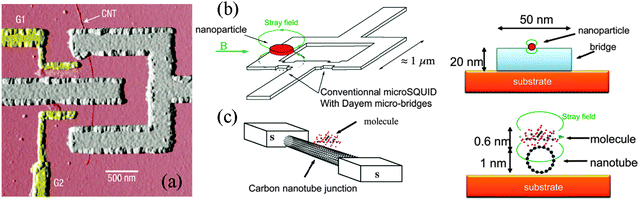 | ||
| Fig. 11 (a) AFM image of a CNT-SQUID device with two lateral gates. The SQUID loop (grey) is interrupted by the two CNT Josephson junctions with a length of about 200 nm. The single-walled CNT with a diameter of about 1 nm was located using an AFM and Pd/Al (3/50 nm) aligned electrodes were deposited over the tube using electron-beam lithography. (b), (c) Schemes of the implementation of the nano-SQUID detection in the near-field regime. (b) Nanoparticle placed on a nanobridge fabricated using state-of-the-art nanolithography and thin film deposition. (c) Molecular magnet grafted on a CNT nanobridge. Panel (a): reprinted with permission from Macmillan Publishers Ltd: Nature Nanotechnology ref. 94, Copyright 2006. Panels (b) and (c): reprinted with permission from ref. 165. Copyright 2009 IOP Publishing Ltd. | ||
The proposal of this new generation of ultrasensitive magnetometers for nanometre-sized samples has opened promising perspectives offered by the combination of CNT based electronics and molecular magnetism, especially in views of the application of molecular magnets in spintronics,166 and remains an open challenge for the following years. Apart from the CNT-based SQUID devices, CNT-FET are also of increasing interest. In these devices, the presence of a molecule grafted on the CNT locally perturbs the electronic states of the semiconductor CNT modifying the transport properties of the hybrid device. CNT-FETs are demonstrated to have single molecule sensitivity, and thus allow the study of the couple strength between the CNT and the attached SMM.101 Very recently, it has been shown that these devices can also act as supramolecular spin valves; the localized magnetic moment of TbPc2 SMM laterally coupled through supramolecular interactions to a single-walled CNT also leads to a magnetic field dependence of the electrical transport through the CNT, giving magnetoresistance ratios up to 300% down to 1 K.167 Thus, it allows electrical detection of the magnetization switching of a single quantum magnet. Finally, the switching of the magnetization of single molecules could also be detected using the nanomechanical properties of a suspended nanotube, which could act as a nanometre-sized vibrating sample magnetometer.168 The motion of the nanotube could be studied by the current through the nanotube itself. However, optimization of such CNT based spintronic schemes requires the improvement of integration methods of the magnetic molecules on the CNT.
Decoration of CNTs magnetic molecules is an active field of research since it is the open issue regarding the integration of the magnetic molecules in CNT based devices.166 Different functionalization methods have been exposed in Section 2.1.3, but still, SMM@CNT detectors and spintronics devices require the sequential addition of a small and controlled number of nanomagnets as well as grafting strategies that minimize the presence of scattering sites, such as the use of non-covalent bonds. To avoid the limitation in the performance of the CNT devices due to defects, Bogani and Wernsdorfer highlighted the fabrication steps needed for obtaining SMM@CNTs hybrids that shall be strongly considered when developing strategies for CNT devices.110
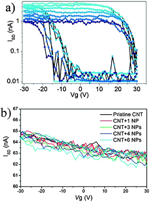
Non-covalent decoration of CNTs has only been performed in solution.100 Bogani et al. used non-covalent π-stacking interactions to graft pyrene-functionalized tetrairon(III) SMM [Fe4(L)2(dpm)6] onto the walls of CNTs, under conditions compatible with the creation of electronic devices.101 The hybrids were produced by immersion of the CNT-FETs in a solution of the SMM, followed by extensive washing. The grafting was reiterated and after each treatment the progressive addition of SMMs was followed by the CNT-based device response, demonstrating the single-SMM sensitivity of CNT-FETs. Even though the π-stacking strategy has been successfully used to graft molecules on the walls of CNTs in solution, the efficacy of this strategy when operating in conditions compatible to the fabrication of electronic devices remains undisclosed. In particular, the authors found that after each treatment, a few SMMs were found to stick onto the CNT, while some others were also located on the surrounding surface of the device, showing only limited specificity of the pyrene-substituted SMM for the CNTs. This inconvenience was overcome later on by Bogani et al., who used van der Waals interactions from ligands containing long alkyl chains to self-assemble magnetic NPs of CoFe2O4 of about 6 nm in diameter onto metallic and semiconductor CNTs, and studied the sequential grafting of the nanoparticles on the transport properties of CNT electronic devices (Fig. 12).102 The hybrids were produced by repeating immersions of CNT based electronic devices into a dispersion of the NPs. While the semiconductor CNT is sensitive to single molecule attachment, the transport properties of a metallic CNT remain unchanged, which is desirable for the use of this grafting technique for the production of CNT-SQUID devices (Fig. 13). Moreover, the use of hydrophobic tails seems more suited for a controlled and selective grafting, and allows an appealing unprecedented sequential grafting of a controlled number of dots to the CNTs. This is of great importance as spintronic devices require the sequential addition of a small but very controlled number of nanomagnets.
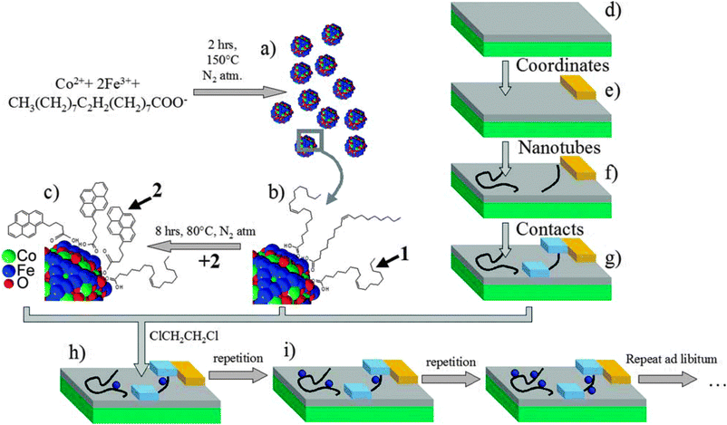 | ||
| Fig. 12 Scheme of the assembly of the hybrid CNT-FET devices with CoFe2O4 NPs. (a) Synthesis of CoFe2O4 NPs. (b) Their surface is functionalized either with oleic acid or (c) with 4-(1-pyrenyl)butanoic acid. (d) Si wafers (green) covered with a SiO2 layer (gray) (e) are used to fabricate gold electrodes (yellow). (f) CNTs are deposited and located with an AFM. (g) Individual CNTs are connected with Pd leads (blue) spaced by 300 nm. (h) Hybrids are assembled by selective grafting of NPs on CNT. (i) Successive depositions allow control over the number of NPs in the hybrid. Reprinted with permission from ref. 102. Copyright 2010 The Royal Society of Chemistry. | ||
 | ||
| Fig. 13 Effect of the CoFe2O4 NPs grafting on the transport characteristics of metallic and semiconducting CNTs. (a) Typical transfer characteristics of a semiconducting CNT-FET hybrid acquired for successive integration of NPs (color scale). (b) Same measurement for a typical metallic CNT-FET at room temperature, for several repetitions of the assembly treatment. Reprinted with permission from ref. 102. Copyright 2010 The Royal Society of Chemistry. | ||
Rod et al. proposed three experimental methods to fabricate nanoscale devices with a CNT bridging metallic electrodes and decorated with magnetic iron/iron oxide nanocubes with a size of 18 nm.169 The decoration of the CNT with iron oxide nanocubes is performed in solution and then the hybrid CNTs are deposited and aligned into the devices by (a) nanomanipulation, (b) drop casting or (c) a technique based on ac-dielectrophoresis.
Finally, another promising in situ deposition technique compatible with UHV characterization techniques uses a spray (or electrospray) to deposit materials on surfaces. This appealing method has been already used for different purposes,110–112,170 and Wernsdorfer et al. proposed to adapt it to deposit molecules directly onto the CNT junction of a CNT-based device.137 The molecular vapour should be directed into the dilution refrigerator, and as soon as a molecule lands on one of the two CNT junctions, the conductivity of the latter changes and the sample holder is confined. Magnetization measurements should then establish whether the molecule is magnetic or not.
At this point, it is worth to emphasize that most transport measurements performed with SMM@CNT-based devices mostly deal with the effect of the SMM attached to the device on its conductive properties. To the best of our knowledge, the first measurement of magnetic properties of a SMM obtained up to now with the use of such devices has been just recently published, and uses the magnetoresistance properties of a CNT based device to electrically detect the magnetic properties of TbPc2 SMM individual molecules.167 Integration of the TbPc2 SMMs was done stochastically by drop casting on a wafer of sensors consisting of single-walled CNTs placed between non-magnetic contacts. The system behaves as a supramolecular spin-valve with very high magnetoresistance ratios and opens up new perspectives for molecular spintronic devices. In a reversed way, the analysis of the differential conductance of the CNT as a function of the temperature and switching-field angle shows the fingerprints of these quantum molecular magnets such as uniaxial anisotropy and quantum tunnelling phenomena.
A new type of SQUID based on graphene has been suggested with potentially high sensitivity to detect single nanomagnets, together with high versatility to fabricate multijunction circuits,171 and it has the conduction layer directly accessible to be functionalized with the magnetic molecules. In this sense, graphene based sensors as dc SQUIDs should be devices with high sensitivity and suitable to easily integrate a wide range of magnetic materials.
On the other hand, in order to increase the sensitivity and spatial resolution of Hall magnetometers, an important issue to improve is the distance between the nanomagnet and the two dimensional electron gas (2DEG) sensing channel. Typically it is located beneath capping and insulating layers to form the well, placing the channel 20 nm or more beneath the sensor's surface. Additionally, such structures have 2DEG layer thickness ranging from 4 to 20 nm, so the rapid decay of the magnetic field within the layer itself would result in a significant reduction in sensitivity eventhough it provides information on the directionality. To overcome this factor, it is proposed to use graphene based sensors instead of 2DEG systems. Graphene's one-atom thick layer directly exposed to the external world, together with its high mobility, can lead to extraordinary magnetoresistance devices that combine Hall effect with geometric magnetoresistance, indeed having a sensing layer of thickness of atomic dimensions located just at the device's surface.172 In this sense, one of the open issues is the integration of the magnetic material on the graphene-based sensors avoiding covalent grafting and, in the case of a Hall gradiometer, with the necessary resolution in positioning to place the material on one cross-section while keeping the other one free of material. With this aim, adapted DPN nanolithography has been successfully employed to selectively deposit Co NPs on a 1 μm2 cross section of a graphene based μHall magnetometer (Fig. 14),173 though the measurement of the NPs is a work still in progress.
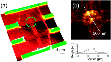 | ||
| Fig. 14 (a) 3-D AFM topography of a graphene-based Hall nanosensor with one cross section (1 × 1 μm2 in size) functionalized with Co nanoparticles, indicated with a green circle. (b) AFM image of the cross section functionalized with Co nanoparticles of 7.6 ± 1.0 nm of diameter deposited with the help of an AFM tip and height profile along the white dashed line in the AFM image. See ref. 173. | ||
Real measurements of electron transport properties of graphene based FETs functionalized with TbPc2 have indeed been performed under ambient conditions and at different TbPc2 SMM concentrations.66 The shift of the minimum of the conductance toward lower gate voltages on increasing TbPc2 SMM concentrations up to a certain point suggests n-doping of the graphene, though no significant disorder to it is induced. Still, for higher concentrations, the presence of clusters and crystallites induces defects and diffusion sites on the graphene sheet and degrades progressively the mobility. More recently, an improved device made by a graphene nanoconstriction decorated with TbPc2 SMM has been successfully used to electrically detect the magnetization reversal of these molecules in the proximity of graphene.174 Changes of magnetoconductivity of the graphene device up to 20% together with hysteresis with the magnetic field are observed due to the magnetization reversal of an average of 10 TbPc2 SMM molecules placed on the graphene nanoconstriction, demonstrating the ability of hybrid spintronic graphene based nanodevices to detect magnetization properties at the single molecule level.
3.3. Single molecule transport measurement hybrid devices
Several techniques are used to study transport properties through single molecules, using different configurations and geometries. For instance, STM has been widely used to perform spectroscopic studies on single molecules as will be shown in Section 4.5, but its two-terminal geometry prevents it from coming into the modulation of the transmolecular conduction. In this regard, three-terminal hybrid devices open a wide range of applications from single molecule transistors to spintronics devices. With this new configuration, the molecule bridges the gap between two electrodes, while a third electrode called gate electrode is used to modulate the conducting properties of the junction, for example by reducing or oxidizing the molecule, or moving the molecular levels with respect to the Fermi energy of the electrodes to allow access to different charge states. This allows spectroscopy measurements of the characteristic excited states of the molecules to be done, from vibrational,175 and electronic excitations,176,177 to states related to spin transitions.178,179 Different approaches have been used to fabricate the nanojunctions of three-terminal devices (Fig. 15),180 the most used being the electromigration technique181,182 that uses a large current density to break a thin narrow wire and form two separated electrodes (Fig. 15a).183 Still, the size and the geometry of the gap formed in this way turns out to be quite uncontrollable. In this case, the substrate can be used as the gate electrode.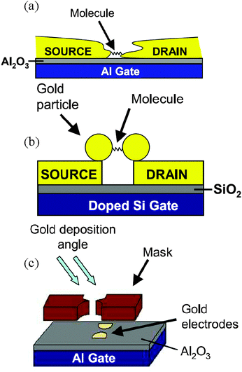 | ||
| Fig. 15 Schematic diagrams of different three-terminal devices. (a) Electromigrated thin metal wire on top of a Al/Al2O3 gate electrode. (b) Dimer contacting scheme, by using dimmers of Au nanoparticles bridged by an organic molecule. (c) Angle evaporation technique to fabricate planar electrodes with nanometre separation on top of a Al/Al2O3 gate electrode. Reprinted with permission from ref. 180. Copyright 2008 IOP Publishing Ltd. | ||
The most difficult step is indeed the integration of the molecule into the gap. In most cases, integration of molecules into nanojunctions is done by immersion of the device in a solution of the target molecules, either before or afterwards the gap formation.178,179,183–186 If the formation of the gap is itself complicated, the integration of the molecule in the device turns out to be completely random, thus leading to the need of testing hundreds of devices before the one with the expected characteristic fingerprints of the molecule on the transport measurements is found.184 An alternative has been proposed by Dadosh et al. based on the synthesis of dimers of gold nanoparticles bridged by an organic molecule (Fig. 15b).187 The integration is done by electrostatically trapping the gold nanoparticles between two metal electrodes, but in this case, the operation of the device seems to be quite affected by the behaviour of the gold nanoparticles themselves.
Different integration experiments insert individual metal–organic molecules into transistor structures for making single molecule transistors.175–177,188 For instance, Heersche and co-workers reported transport measurements through SMM in a single molecule transistor geometry (Fig. 16a–c).178 First, thin gold wires (∼10 nm) were fabricated by e-beam lithography on the top of an Al/Al2O3 gate. After cleaning treatments, the samples were soaked in a solution containing the SMM clusters. Then, electromigration181 produced nanometre-scale gaps in the gold wires in which the SMM were trapped. In this case, a derivative of the Mn12 cluster bearing acetyl-protected thiol end-groups was used, which bound the SMM to the gold electrodes by means of covalent bonds. Another experimental realization of this scheme has been described by Ralph and co-workers, who reported single molecule transistor measurements on devices incorporating SMM (Fig. 16d).189 In this case, native Mn12 clusters were directly adsorbed on the Au wires, but only found evidence of magnetic anisotropy in some of the studied molecules, meaning that molecular magnetism was usually destroyed during the device fabrication. Similar stability was shown for thiophenecarboxylate functionalized Mn12 derivatives inserted in a single-electron transistor (SET) device,183 for which many molecules were not stable enough to be measured for long periods of time. Still, del Barco and co-workers were able to show the typical Coulomb diamond response of this molecular SET.
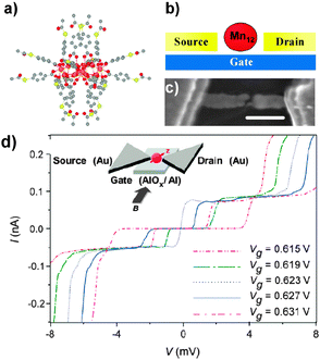 | ||
| Fig. 16 (a) Side view of a Mn12 molecule with tailormade ligands containing acetyl-protected thiol end groups (R = C6H4). Atoms are color labeled: manganese (orange), oxygen (dark red), carbon (gray), sulfur (yellow). The molecule diameter is about 3 nm. (b) Schematic drawing of the Mn12 molecule (red circle) trapped between electrodes. A gate changes the electrostatic potential on the molecule enabling energy spectroscopy. (c) Scanning electron microscopy image of the electrodes. The gap is not resolvable. Scale bar corresponds to 200 nm. (d) Current–voltage (I–V) curves at selected values of gate voltage (Vg) for a Mn12Ac transistor at 300 mK. (Inset) Schematic of a SMM transistor. Reprinted panels (a)–(c) with permission from ref. 178. Copyright 2006 by the American Physical Society. Reprinted panel (d) with permission from ref. 189. Copyright 2006 American Chemical Society. | ||
More recently, electron tunnelling spectra of N@C60 magnetic molecules were measured in a single molecule transistor geometry.185 They proved that the magnetic character of the molecule was preserved together with the capability of making good electrical contact with the individual magnetic molecule, which provides the basis for advanced strategies to electronically manipulate the spin state of molecules in hybrid devices. In this sense, van der Zant and co-workers have just proved the ability to control the high-spin to low-spin transition of a single Mn2+ ion integrated in a three-terminal device with the gate voltage, by reducing the coordinated ligand.186 In a step forward,184 they showed electrical control on the single molecule magnetism of individual Fe4 SMM embedded in a three-terminal device geometry; reduction or oxidation of the molecule induced by the gate voltage is found to even enhance the magnetic anisotropy of the SMM as probed by inelastic tunnelling spectroscopy measurements with the device.
Finally, a molecular switching device made by contacting individual nanoparticles based on spin-crossover molecules between nanometre-spaced electrodes has recently been reported.14Nanoparticles of ca. 11 nm diameter of Fe(II) coordination polymer [Fe(trz)3](BF4)2 (trz = triazole) have a spin cross-over Fe(II) core coated with an organic shell and show a cooperative spin transition from Fe(II) low spin, S = 0, to high spin, S = 2, above room temperature, with a hysteresis of about 40 K of width. A monolayer of NPs was deposited over a set of conductive devices by contact printing, and the presence of one or several particles in parallel contacting the electrodes was observed as a clear increase in the conductance between the electrodes. Thermal hysteresis in the conductance measurements in such devices was observed over room temperature, resembling that of the magnetic susceptibility measured in the aggregates, and suggesting that the intrinsic spin-crossover properties of the particles are the origin of the observed electrical bistability. Such a device has been proposed as an attractive bistable memory element for which the magnetic state can be controlled electrically.
4. Magnetic characterization techniques
The wide majority of magnetic characterization of SMMs has been done up to now in bulk crystalline samples with techniques such as SQUID magnetometers or Hall sensors. SQUIDs, based on superconducting loops containing Josephson junctions, are the most sensitive magnetic flux detectors and the most widely extended technique for magnetic characterization of materials, since together with their high sensitivity, commercial SQUID devices can easily operate in a wide range of temperatures down to the mK regime and under any kind of external applied magnetic fields. There are only a few general restrictions over the size and the shape of the sample, thus allowing the characterization of most types of magnetic materials. Measurements of SMMs are affected by the crystallinity degree of the sample, the relative orientation of the molecular axis in the crystal or the need to have enough material to give a minimum intensity of the signal, preventing most of the times the use of a single crystal when it is not big enough. Magnetometers based on the Hall effect have also emerged as an important magnetic measurement technique; they have been shown to be very sensitive, small sized and versatile, since they can be used in a wide range of temperatures and virtually without any limitation in the applied external fields. Other techniques such as Electron Paramagnetic Resonance (EPR) or High Field EPR (HFEPR) are also commonly used for the study of the magnetocrystalline anisotropy in SMMs.As we have seen in Section 3, the need to study crystalline nanoparticles as well as structured materials on surfaces, including the magnetic phenomena of individual single molecules, has promoted the miniaturization of SQUIDs and Hall sensors to increase their sensitivity up to the single molecule level. Most devices have not achieved this limit yet, but sensitivity of one or few magnetic nanoparticles is already available. As a consequence, miniaturization of flux detectors has led to the need for development of integration techniques that allow the fabrication of hybrid devices, and in a near future, also its use in applications such as spintronics,22 computation,18–21 high density magnetic storage,16 biosensing or even molecular magnetic cooling.23,24 The use of hybrid devices such as nanoSQUIDs or single molecule transport measurement devices for the study of SMM at the single molecular level has been reviewed in Section 3, since in this case, the integration of the magnetic material in the device plays an important role as has been specifically analysed.
The assessment of the SMM magnetic behaviour of a 2D assembly of molecular magnets on a surface is really challenging due to the weakness of the magnetic signal to be measured. Typically, the structural and chemical characterization of bidimensional assemblies of molecular magnets is done by STM, XAS, XPS and RPES while different magneto-optical techniques have been extensively used to address their magnetic properties.
A complementary approach to the use of nanoSQUIDs or nanoHall sensors for the magnetic characterization of SMMs on surfaces is based on the use of a broad range of characterization techniques traditionally applied in surface science that are also suitable to study the magnetic properties of SMMs and magnetic molecular materials on thin films or deposited on surfaces. Among these techniques, we can find magnetic resonant techniques covering a wide range of the electromagnetic spectra, from the microwaves used by EPR or NMR, to the optical waves used by MCD or MOKE, and also the X-ray radiation obtained from synchrotron facilities, that enable to perform XMCD studies. Finally, we find typical surface characterization techniques with atomic resolution such as STM or SPM in general, including MFM or Scanning Hall Probe Microscopy (SHPM) and Scanning SQUID Microscopy (SSQM).
Despite the wide list of available magnetic characterization techniques, not all of them have been applied for the study of individual SMMs or SMMs grafted on surfaces. XMCD (due to its surface degree of sensitivity) and MCD have been up to now the preferred techniques to study the magnetic features of archetypal SMMs like Mn12 or Fe4 on surfaces or embedded in matrices. There have also been punctual attempts to apply other surface magnetization sensitive techniques such as β-NMR or low-energy muon spin resonance (LE-μSR) that, though suitable for studying SMMs on surfaces, have not yet been really exploited. Still, it is only possible to apply other techniques such as HFEPR or the so-called Frequency Domain Magnetic Resonance Spectroscopy (FDMRS) to the study of SMMs in the case of frozen solutions, polymeric matrices or thick films, when the available magnetic signal is enough to achieve the detection limits.
Scanning Probes Microscopies are another family of techniques that show high resolution on surface characterization, and that can be implemented to study magnetic features. These range from STM to MFM, and include SHPM or SSQM.
STM has been probed to be a technique with atomic resolution and capable of detecting single magnetic moment on surfaces. Still, this high sensitivity is only achieved under UHV conditions and at low temperatures, that entail restricting conditions over the samples to be measured. In this sense, deposition techniques that are compatible with UHV conditions need to be applied, and this has limited the studies mainly to families of SMMs and magnetic molecular materials such as metal phthalocyanines or lanthanide phthalocyanines.
Finally, other SPM techniques with nanometric resolution such as MFM or SHPM have indeed been applied to the characterization of SMMs on surfaces such as Mn12 or prussian blue analogues thin films. We believe that regardless of not being yet extended, they have intrinsically a strong potential to be applied to the study of the magnetic features of SMMs on surfaces.
In this section, we will review all these general techniques for surface characterization that either have been applied to the study of magnetic properties of nanostructured SMMs on surfaces and in matrices or we think they have the potential to be applied. We will first describe the state of the art of each technique together with its capabilities and we will then give the available examples on SMMs studies.
4.1. Hall magnetometers
Micro-Hall magnetometry is based on high mobility semiconducting heterostructures with channels forming a 2DEG; the method measures the Hall response of the 2DEG to the small dipole field from the magnetic entities. The best performances in terms of magnetic flux sensitivity have been obtained with GaAs/AlGaAs heterostructures, with the 2DEG buried 50–100 nm below the surface, that combine small carrier concentration and high mobility.190Nanometre-sized Hall magnetometers have been proposed as possible tools to detect single-electron spin and perform quantum measurements on qubits.191 However, 2DEGs are extremely sensitive to patterning that induces charge depletion for lateral probe sizes below 1 μm, and, in practice, limits the applications of such devices with respect to temperature and lateral size. Many research efforts have been done to investigate different materials and procedures for the fabrication of submicron Hall probes that may overcome the limitations of the GaAs/AlGaAs heterostructures and combine spatial resolution in the nanometre range and high magnetic sensitivity, even at room temperature. Among them are the use of >100 nm thick films to overcome the problem of charge depletion, or the use of other materials as an alternative for 2DEG probes, such as semimetal Bi films, metallic Au films192 or semiconducting Si-doped GaAs,192 InAs,193InSb,194 and In0.75Ga0.25As films195 or granular Co–C films.196
Marked improvement in magnetic moment resolution, especially at high fields, can be realized by using Hall gradiometry in which an empty Hall cross with opposite current flow is employed to circumvent the difficulty of measuring a tiny signal on the top of a much larger background (see Fig. 17).197,198 Kent et al. detected and characterized arrays of nanometre scale diameter Fe nanoparticles of different shapes with a GaAs/GaAlAs micro-Hall gradiometer,197 grown by STM assisted chemical vapour deposition199 directly onto one of the cross sections of the Hall gradiometer. Later on, Liet al.198 were able to measure the magnetization switching in the easy magnetization axis of a single Fe nanocylinder of 5 nm diameter and 120 nm high, with an estimated magnetic moment of 5 × 10⁵μB at 77 K, placed in the centre of the sample cross section of 600 nm × 600 nm, just over the highest sensitivity zone. The cylinders were directly grown onto the cross section by STM assisted chemical vapour deposition from the precursor iron pentacarbonyl Fe(CO)5 by applying a bias voltage of 217 V between the tip and the substrate. The tip was then progressively moved to different spots over the cross section to cover the maximum possible area.
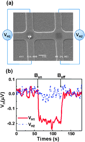 | ||
| Fig. 17 (a) SEM image of a micro-Hall device that was patterned from an InAs QW wafer viaphotolithography and wet etching, then coated with an insulating layer of SiO2, followed by a Au layer for molecular interfacing. MHA was patterned by DPN and then biotinylated and is evident as dark squares in the central, active regions of the Hall crosses; the surrounding Au surface was passivated with ODT. Three streptavidin-coated magnetic beads assembled on the biotinylated region of the left cross. (b) ac Hall voltage as a function of time for the two crosses shown in (a). Due to the presence of magnetic beads on the left cross, the ac Hall voltage VH1 (red) decreased by ∼0.19 μV when a dc magnetic field B = 70.6 mT was applied. In contrast, no change in Hall voltage VH2 (blue) was observed when B was applied to the empty cross. Reprinted with permission from ref. 204. Copyright 2009 IOP Publishing Ltd. | ||
Hall devices have been applied for the measurements of a large variety of materials including superconductors, ferromagnetic particles, ferrofluids,200 and patterned submicron- or nanomagnets,197,198 but to the best of our knowledge, no examples of magnetic characterization of SMM either grafted on surfaces or in the form of monolayers are found in the literature. Instead, they are specially appealing for applications in magnetic biosensing201 using superparamagnetic labels (i.e. magnetic beads made of a large superparamagnetic nanoparticles with diameters <15 nm, typically of Fe3O4 or γ-Fe2O3, dispersed in a micrometric spherical polymer matrix202,203) due to its exceptional magnetic moment sensitivity over a large dynamic field range. The beads surface is biologically functionalized with the adequate linker molecules and in this way, they provide selective biomolecular binding to the specific target (Fig. 17).204
4.2. Magnetic resonance techniques
Magnetic resonance techniques have been widely used for the characterization and the study of magnetic properties of SMM in bulk, that is, on large single crystals. Conventional NMR205–210 and Muon Spin Rotation (μSR)205,209,211,212 have been used to measure molecular spin dynamics down to the quantum regime. On the other hand, EPR and HFEPR (see for example ref. 213–219) have been extensively used to characterize the anisotropy parameters of all kinds of SMM and molecular magnetic materials. Still, the small quantity of material available in the case of thin films of magnetic molecules or nanostructured molecular materials on surfaces makes it almost impossible to apply these conventional bulk techniques for its magnetic characterization, and further developments are needed. Some interesting variations of these techniques that could be envisaged for further experiments on SMMs on surfaces include the detection of EPRvia magnetization measurements with a Hall probe magnetometer,220detection of the magnetization transitions in a sample by microwave absorption experiments in a resonant cavity,221 or combination of surface acoustic waves with HFEPR measurements.218A few examples of EPR measurements on SAM are available in the literature. Veciana and co-workers measured the EPR spectrum at room temperature of bistable organic PTM radical derivatives (bearing a thioacetate and a disulfide group) in the form of SAM on a surface area of 66 mm2 and contrasted it with a spectrum of the same SAM of a PTM anion.15 Paramagnetic behaviour of the PTM derivative SAM in the radical form was confirmed by a g value of 2.0026, while the anionic counterpart, after switching the SAM to its anion state, did not give any signal due to its diamagnetic nature. Later on, similar studies were performed on SAMs of tris(2,4,6-thrichlorophenyl)methyl radical (TTM) derivatives, whose magnetic nature was first confirmed by EPR at room temperature before using the samples for Electron Spin Noise–STM experiments (Fig. 18).222
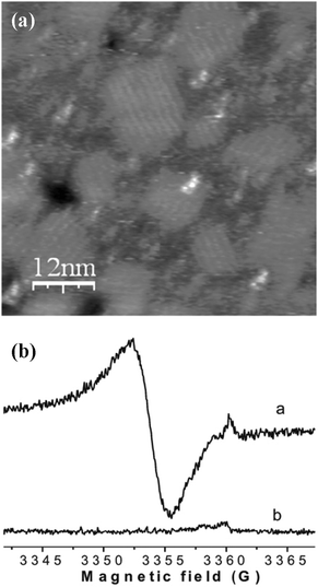 | ||
| Fig. 18 (a) STM image (60 × 60 nm) of TTM dispersed on Au(111). Tip sample bias 0.3 V and tunnelling current 15 pA. (b) a. EPR spectrum of the dip and rinse TTM sample; b. EPR spectrum of the gold/mica substrate. Experimental parameters: MW frequency 9.40388 GHz, power 20 mW, mod. amp. 1 G, field modulation frequency 100 kHz. g-value 2.00343. EPR cavity: standard TE102. Panel (a): reprinted with permission from ref. 32. Copyright 2009 The Royal Society of Chemistry. Panel (b): reprinted from ref. 222, Copyright 2009, with permission from Elsevier Masson SAS. | ||
Depth-resolved β-NMR measurements have been applied for the study of the magnetic properties of a monolayer of Mn12-ac molecules grafted on a Si substrate (Fig. 19),228 demonstrating the competence of this technique for the characterization of monolayers of magnetic molecules. From such measurements it can be deduced that the magnetic properties of Mn12-ac molecules were lost in translation from bulk to surface-grafted and dramatically affected by its interaction with the substrate.
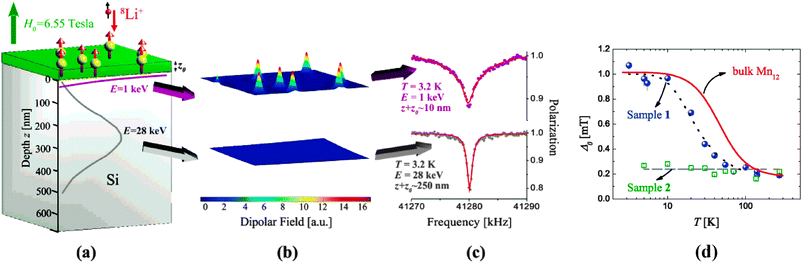 | ||
| Fig. 19 (a) A schematic of a sample of Mn12 molecules grafted on a Si substrate. The stopping profiles of 8Li in Si at E = 1 and 28 keV are also shown (purple and gray lines, respectively). (b) The simulated dipolar fields from the Mn12 monolayer calculated near the surface (top) and deep within (bottom) the Si substrate (arbitrary units). (c) The measured β-NMR spectra of the Mn12 monolayer in an applied magnetic field H0 = 6.55 T at T = 3.2 K. The top spectrum is for E = 1 keV and the bottom for E = 28 keV. The solid lines are fits to the calculated resonance line shape, and extract Δ0 as the width of dipolar field distribution, which is proportional to the magnetic moment of Mn12 molecules. (d) The measured broadening Δ0 in a sample of Mn12 molecules grafted on a Si substrate (sample 1, circles) and a clean Si substrate (sample 2, squares) as a function of temperature at E = 1 keV. The solid line is the measured magnetic moment in bulk and the dotted line is a guide to the eye. The dashed line represents the average Δ0 measured in the control sample 2. Reprinted with permission from ref. 228. Copyright 2007 American Chemical Society. | ||
4.3. Magneto-optical techniques
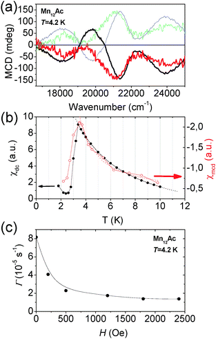 | ||
| Fig. 20 (a) MCD spectra of Mn12-ac in a frozen solution of CH2Cl2∶tol 1∶1 (black and blue lines) and CH3CN∶dmf 1∶2 (red and green lines) at H = 104 Oe (black and red) and H = −104 Oe (green and blue). (b) ZFC measurements of Mn12-ac in 1∶1 glass of CH2Cl2∶tol, with an applied magnetic field of H = 103 Oe. Solid circles indicate SQUID measurements (referred to the left axis) and open red circles stand for MCD measurements (referred to the right axis). (c) Relaxation measurements of the MCD signal at T = 4.2 K. The figure shows the adjusted MCD decay rate as a function of the applied magnetic field during the relaxation. The increase of the MCD signal decay rate at low fields is indicative of acceleration of the magnetization due to resonant quantum tunneling (see ref. 232). | ||
More recently, Bogani et al. applied this methodology to study different derivatives of Mn12 in different environments such as an amorphous matrix, Langmuir Blodget film or directly grafted on Au surfaces (Fig. 21).239 They were able to probe that while the Mn12 molecules can also retain the SMM behaviour in the polymeric matrices, eventually the SAMs of SMMs grafted on gold do not retain the hysteretic behaviour over the typical temperature range but a paramagnetic signal. Later on, Novak et al. performed similar studies on Fe4 molecular clusters diluted in different polymeric matrices.240 They compared the field dependence of the magnetization data and the MCD signal at different wavelengths at 1.55 K. Since circularly polarized light of different wavelengths excites different electronic transitions, only those electronic transitions corresponding to the Fe4 cluster ground state were sensitive to its paramagnetic behaviour and showed saturation as a function of the magnetic field. Slight differences among the magnetization and MCD signal field dependence were ascribed to possible cluster orientation effects arising from strains induced by the polymeric matrix during the preparation process. Finally, thin films of Mn12-ac deposited by a vacuum spray deposition technique on transparent LiF substrates were also studied by MCD.110 Magnetic field dependence of the MCD signal of a 20 nm film shows hysteretic behaviour with similar coercive field and shape than the one measured with SQUID for thicker films. This fact assesses the preservation of the SMM behaviour of the Mn12 molecules deposited on the LiF substrates.
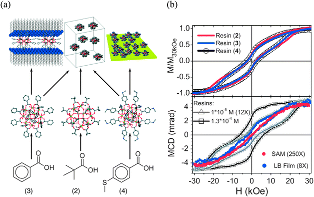 | ||
| Fig. 21 (a) Representation of the Mn12 derivatives studied by Bogani et al. in different non-crystalline environments. The lower row represents the schemes of the ligand molecules used to substitute the acetate ligands of Mn12-ac. The middle row represents the structures of the substituted clusters, as viewed along the molecular fourfold symmetry axis. The structures of (3) and (4) are obtained from previously reported X-ray data, while (2) is modeled by minimizing steric encumbrances, as no crystal structure is reported for the derivative. Oxygen atoms are red, carbon atoms grey, sulfur atoms blue, manganese centers green, and hydrogen atoms have been omitted for clarity. The last row schematically depicts the noncrystalline environments in which the molecules are organized: a LB film, on the left, the siloxanic resin in the middle, and a SAM on the right. (b) (Top) Hysteresis loops recorded with the VSM setup for samples of (2) (red line), (3) (blue line), and (4) (black circles and line) included in the 3D amorphous environment. All measurements were performed with a field-sweep rate of 10 kOe min−1 at T = 1.5 K and were rescaled to the signal at 30 kOe for better comparison. (Bottom) MCD signal acquired for the different materials as a function of the magnetic field. The same field-sweep rate of 10 kOe min−1 and the same wavelength of 632.8 nm were used for all samples. Black line and squares: (2) included in the siloxanic resin with C = 1.3 × 10⁻⁴ M at T = 1.45 K. Gray line and triangles: (2) included in the siloxanic resin with concentration C = 1 × 10⁻⁵ M at T = 1.65 K, magnified 12 times. Blue line and circles: 58 layers of a LB film of (3) on quartz magnified 8 times at T = 1.65 K. Scattered red circles: 5 superimposed plates of (4) grafted on gold, magnified 250 times, T = 1.65 K. Reprinted with permission from ref. 239. Copyright 2007 Wiley-VCH Verlag GmbH & Co. KGaA. | ||
4.4. X-Ray based techniques
Mannini et al. were the first ones to use the XMCD on Mn12 adsorbates249 to probe the remanence of SMM behaviour of the deposited molecules on Au.51 By performing XMCD measurements at sub-Kelvin temperatures, they again concluded that significant modifications of the electronic and magnetic structures occur when Mn12 is adsorbed on gold. The redox instability of Mn12 complexes on gold surfaces results in a partial reduction of metal ions to Mn2+, accompanied by structural rearrangements and the loss of magnetic hysteresis. However, the existence of additional experimental parameters that also favour the Mn12 degradation cannot be discarded at this point. Among them, there is the question whether the XMCD technique would be intrinsically unsuited for this kind of measurements, since exciting the core electrons of the molecule could be equivalent to demagnetizing it. Another exposed reason is that the steric constraints generated by the surface distort the cores of the molecules which then loose their SMM properties at 2 K.243 In this sense a possible mechanism could be the induction of Jahn–Teller isomerism responsible for the lowering of the blocking temperature as compared to that of the bulk. For this reason, the magnetization curve displays no hysteresis even though in some conditions the Mn12 molecules seem to be structurally undamaged.243
In a follow-on study, Maninni et al. showed that by comparison with Mn12, the Fe4 SMMs could possibly survive to the deposition process (Fig. 2).250 Even though the films were a few hundred nanometres thick and therefore not monolayered, they achieved surface sensitivity by using the Total Electron Yield (TEY) detection mode. Therefore, they were able to probe the butterfly shaped hysteresis cycle of a single SAM of Fe4 molecules on a Au(111) surface with XMCD synchrotron based techniques down to 0.5 K (Fig. 2c).58,60 More recently, it was used to probe the ferrimagnetic spin structure in the S = 5 ground state of Fe4 SMMs covalently grafted on Au(111) in one step using 1,2-dithiolan-3-yl side groups.61
At the same time, Corradini et al. also studied the electronic structure and magnetic properties of sML distributions of isolated molecular Cr7Ni antiferromagnetic rings deposited on Au(111) surfaces by XAS and XMCD.64 By comparison with previous studies of bulk like samples in the form of polycrystalline thick films only small differences in the magnetic properties arising from a decrease of the exchange coupling constant between the Cr and Ni ions (JCr–Ni) that becomes smaller than that of the Cr ions (JCr–Cr) were detected. This difference in the magnetic properties is unlikely associated to breaking of the bonds within the ring or direct interaction of the metal centres with the gold surface but indeed can easily be explained by a small distortion of the rings. Even though such distortion produces a compression of the energy levels spectrum, the magnetic structure of Cr7Ni–Piv remains substantially the same upon deposition on a surface. Moreover, systematic studies on different functionalization pathways to graft the molecular Cr7Ni rings onto the Au surface from the liquid phase demonstrated its influence on the magnetic properties allowing a minimization of the perturbation (Fig. 22).65
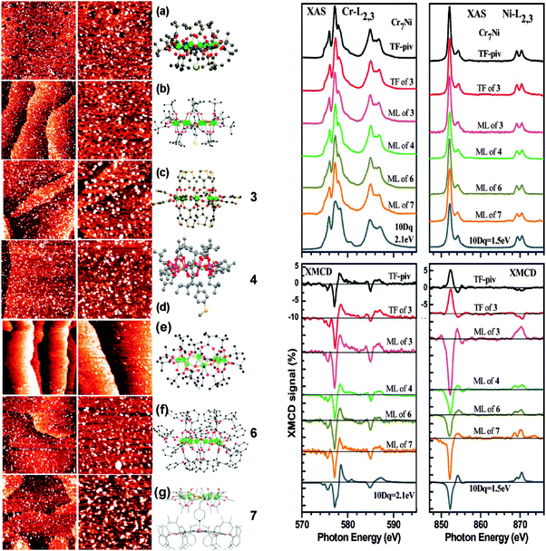 | ||
| Fig. 22 Constant-current (30 pA, 2 V) STM images of the Au(111) surface immersed for 10 min in a 5 mM solution of 4 S-derivatives and 3 S-free derivatives of Cr7Ni AFM rings; (a) Cr7 Ni-thio and (b) Cr7Ni-thiobutane with a single alkanethiol attached to the central ammonium cation, (c) Cr7Ni-3tpc with sixteen 3-thiophenecarboxylate ligands, (also sample 3) (d) Cr7Ni-4mtpp with one peripheric 3-4-methylthiophenyl-propionate (MTPP) ligand, (also sample 4) (e) Cr7Ni-pyridine with pyridinic ring (C5H4N) attached to the central ammonium cation, (f) Cr7Ni-phenoxy, with 16 phenoxybenzoate ligands, (also sample 6) (g) CoPc–Cr7Ni where the Cr7Ni ring is attached, through pyridine group, to the Co ion embedded in a phthalocyanine (CoPc) (also sample 7). Left panel shows an area of 200 × 200 nm2 and central panel shows 100 × 100 nm2. The white entities represent the grafted clusters. In the right panel the structures of the derivatives. The graphs on the right side are Cr (left panel) and Ni (right panel) L2,3 XAS and XMCD spectra for the monolayers (MLs) of 3, 4, 6 and 7, compared with the thick films (TFs) of 3 and of the pristine Cr7Ni–pivalate measured at 10 K and 5 T. The TT multiplet calculations with 10 Dq = 2.1 eV for Cr3+ and 10 Dq = 1.5 eV for Ni2+ are also shown. Reprinted by permission from ref. 65. Copyright 2010 The Royal Society of Chemistry. | ||
Finally, Moro et al. compared the XMCD spectra of sML of Mn6-tpc55,56 with those of relatively thick films,251 and observed a decrease in the average MnIII spin magnetic moment of the sML due to local distortions of the Mn environments and modified Mn–Mn exchange couplings when the Mn6 clusters are deposited on the Au surface, though the oxidation state of MnIII is still preserved. The authors suggest that these distortions might arise from the formation of covalent bonds between the Mn6 and the surface and/or the lack of isotropic interactions with the surrounding molecules, but that this is not enough to question the robustness of the Mn6 core for further developments.
All these results pointing to the survival of the magnetic properties of SMMs when deposited onto surfaces probe that there are no fundamental reasons that preclude the observation of magnetic hysteresis when SMM are wired to a conducting substrate. Moreover, they also can preserve their quantum behaviour; XMCD-detected hysteresis loops of monolayers of oriented Fe4(L)2(dpm) with short aliphatic chains on Au surfaces gave evidence of resonant quantum tunnelling of the magnetization as shown by characteristic steps of the hysteresis cycle (Fig. 2).127 This observed acceleration in the dynamics for certain fields applied along the easy axis was dependent on the relative orientation of the external applied magnetic field and the normal to the surface, and directly implies ordering of the magnetic easy axis direction with respect to the surface.
The metal–porphyrins and metal–phthalocyanines families are magnetic molecules that have also been recently taken into consideration as hybrid systems combining metal and molecular layers for their possible use in molecule-based devices. Even though formally they have not been classified as SMMs, these molecules show excellent chemical stability and furthermore they easily organize in perfect 2D networks by spontaneously ordering through lateral hydrogen bonds, thus becoming a good archetypal family of metal–organic semiconductors. XMCD has been used to study the interaction between different types of paramagnetic porphyrin molecules and ferromagnetic substrates.252 In the case of a Fe octaethylporphyrin (OEP) chloride molecule, Wende et al. demonstrated that owing to an indirect superexchange interaction between Fe atoms in the molecules and atoms in the substrate (Co or Ni) the paramagnetic molecules can be made to order ferromagnetically (Fig. 23).36 The Fe magnetic moment can be rotated along directions in plane as well as out of plane by a magnetization reversal of the substrate. More recently, Bernien et al. went a step forward and demonstrated that the interaction could be modulated; antiferromagnetic coupling between paramagnetic Fe–porphyrin molecules and the Co and Ni magnetic films can be established by an intermediate layer of atomic oxygen.253 Finally, Stepanow et al. proved that the local CuPc magnetic moment survives the interaction with the electronic states of an Ag substrate by angle-dependent XMCD and multiplet calculations.254 Moreover, an enhanced susceptibility with respect to bulk is observed, which arises from extraordinarily strong Cu spin dipole moment anisotropy, up to two times larger than the isotropic spin moment, and a huge orbital-moment anisotropy, that induces a change of up to 500% in the orbital moment from the in-plane to the out-of-plane direction.
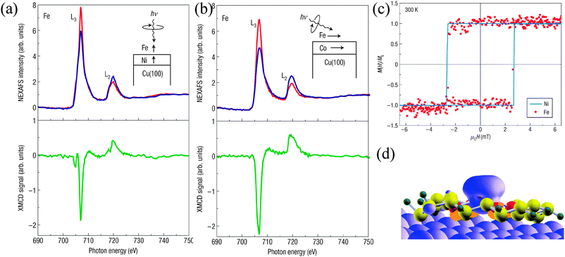 | ||
| Fig. 23 (a), (b) Element-specific magnetic properties of the Fe OEP molecule on ferromagnetic substrates determined by XMCD. X-Ray absorption coefficients for right and left circularly polarized X-rays μ + (E) (red) and μ − (E) (blue) (top) and XMCD (bottom) of the central Fe atom of the OEP molecule on Ni (a) and Co (b) substrates (300 K, 10 mT). The insets depict the orientation of the sample to the incident X-rays. The arrows for Fe and the ferromagnetic films show the alignments of the spins. (c) The element-specific field dependence of the magnetization of the Fe atoms in the molecule and the ferromagnetic substrate (Ni). Hysteresis curves of the Fe atom (filled squares) and Ni (full line) obtained by the L3 edge XMCD maxima of Fe OEP on Ni/Cu(100) at 300 K. (d) Scheme of the Fe OEP molecule placed on the Ni surface. Reprinted by permission from Macmillan Publishers Ltd: Nature Materials ref. 36, Copyright 2007. | ||
More recently, XMCD has been applied to assess the slow relaxation of the magnetization of monolayers and sML of the double decker SMM TbPc2 deposited on Cu,115Au255 and graphite surfaces,256,257 in its neutral and anionic derivatives. First measurements of field dependent XMCD properties on Cu confirmed the retainment of the magnetic anisotropy of the molecules on the surface but did not show any hysteresis of the XMCD signal as a function of the magnetic field.115 This fact was attributed to the long time-scale of a typical XMCD magnetization curve measurement, but when performing the same characterization on neutral TbPc2 thin films and thick films on Au,255 hysteresis is observed in both cases under T = 8 K and 15 K respectively. Butterfly-shaped hysteresis at T = 7 K was also confirmed for double decker SMM TbPc2 monolayers on HOPG, supporting that its intimate contact with graphite does not destroy its SMM behaviour.256,257
4.5. Neutron diffraction
Neutron scattering is extensively used to characterize magnetically ordered solids. Advances in technology improving detection methods, such as the use of multi-detectors, have allowed the application of this technique to study several different magnetic molecular materials, where the intensity of the magnetic signal is rather weak.258 Still, it shows some disadvantages that have prevented the extended use of this technique for the characterization of molecule-based magnetic materials259 such as the need for large amounts of material, the overlap of structural reflections in the region where magnetic reflections mainly occur, due to the typical low-symmetry large unit-cells that these compounds have, and the large incoherent scattering arising from the huge amount of H-atoms contained in the organic ligands, that can only be avoided with the use of deuterated derivatives of the organic samples. Neutron powder diffraction has been successfully used to determine both long-range and short-range magnetic ordering in organic magnetic materials.259,260 Besides, polarized neutron diffraction analysis allows the separation of magnetic scattering from nuclear scattering and has been applied to determine the spin density distribution in pure organic ferromagnets261 and polynuclear clusters.262 Regarding SMMs, neutron diffraction measurements allowed for example to determine the ferromagnetic long-range ordering of Mn12 acetate SMM single crystals263 and the low energy spectrum of Tm-based double-decker phthalocyanine (TmPc2) complex, also in the shape of big single crystals.264 On the other hand, inelastic neutron scattering (INS) allowed to do spectroscopic studies of the anisotropy splitting of SMM such as fully deuterated Mn12-ac, leading to magnetic relaxation measurements,265 the determination of exchange-coupling constants and spin density maps266 or the effect of pressure on the anisotropy of SMMs,267,268 and the excitation of spin waves in molecular rings.269,270 To the best of our knowledge, to date there are no works regarding the study of magnetic properties of magnetic molecular materials deposited on surfaces. The main reasons might be the weakness of the signal provided by surface samples together with the low surface sensitivity of neutrons but still, further development of technology for neutron based analysis techniques could overcome these disadvantages and allow magnetic surface analysis.4.6. Scanning tunnelling microscopy
STM is a technique with atomic resolution based on the measurement of the tunnelling current passing from a metallic tip to a conductive substrate through a sample. In this sense, it is not a technique that directly measures the magnetic features of an atom or molecule, but these properties can be inferred from the conductive measurements. For example, an indirect way to detect the presence of a magnetic moment is through the Kondo effect, that is, the screening of localized individual spins by the interacting metallic conduction electrons of the substrate.On the other hand, most of the examples of measurements on magnetic molecular materials found in the literature are on metal phthalocyanines (MPc) or lanthanide phthalocyanines (LnPc), and double decker phthalocyanines LnPc2 (only some of which do show SMM behaviour). That is because the UHV conditions that need to be applied to use this technique entail restricted conditions to the suitable deposition techniques, and as a consequence limit the availability of samples to be measured. On the other hand, it is also critical that the molecules have good conductive coupling with the substrate in order to perform good STM measurements. In this sense, if the molecules are grafted to the surface through a linker, this must be conductive and must provide good electrical coupling.
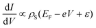
I–Vspectra were recorded by Burgert and co-workers on Mn12 derivative [Mn12O12(O2CC6H4F)16(EtOH)4]·4.4CHCl3 on a Au surface functionalized with two types of short and highly conductive molecules: 4′-mercaptooctafluorobiphenyl-4-carboxylic acid (4-MOBCA) and 4-MTBA.70 The use of these molecules ensured both the grafting of Mn12 clusters and the optimal electronic coupling of the SMM with the surface.69 Indeed, it was observed that 4-MOBCA was more advantageous to obtain the STS spectra due to the lack of observed instabilities at high bias voltages compared to the 4-MTBA molecule (Fig. 24). From the symmetry of the STS spectrum, the EF–HOMO difference was estimated to be 0.5 ± 0.2 eV, even though no detailed electronic structure of the molecules was obtained from these measurements.
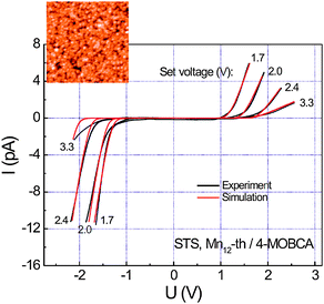 | ||
| Fig. 24 STS spectra obtained from Mn12-th at different set voltages (black) and corresponding spectra obtained from the simulations (red). A higher set voltage in STS measurements corresponds to a larger distance between tip and molecule. The inset shows an 100 × 100 nm2STM images of Mn12-th deposited on the 4-MOBCA functionalized Au(111) surface. Reprinted with permission from ref. 69 and 70 (main panel and inset, respectively). Copyright 2008 the American Physical Society and 2007 the American Chemical Society, respectively. | ||
Kondo effect. A way to obtain magnetic information from STS measurements is the study of the Kondo effect. The Kondo effect describes the scattering of conduction electrons in a metal due to magnetic impurities or localized spins; as the temperature tends to zero the magnetic moment and conduction electron moments bind very strongly to form an overall non-magnetic state that becomes effective below a critical temperature called Kondo temperature (TK). This temperature indicates the thermal range of stability of the Kondo singlet, and is dependent on the strength of the exchange interaction between the local magnetic moment in the molecule and the conducting electrons. The Kondo effect produces a pronounced resonance in the local density of states (LDOS) near the Fermi level that can be detected by low-temperature STS. In this way, magnetic configuration of localized spins, such as transition metal ions in a host molecule can be elucidated via the Kondo resonance in cryogenic STM.271–273 Most of the previous studies on the Kondo effect have focused on magnetic atoms on open metal surfaces that typically show very low Kondo temperatures. On the other hand, studies on molecular Kondo effects of magnetic atoms caged in a molecule such as MPc or LnPc, where M = Co, Fe and Ln = Tb(III) show an increase of TK.113,271,274,275 In these cases, control over the Kondo resonance properties has been achieved in many ways; by changing the ligand and the molecular structure (Fig. 25),271,272 by manipulating the nearest neighbour molecules273 (Fig. 26) or the adsorption site of the molecule with the STM tip and thus changing the molecular conformation,274 or even through quantum size effects generated by thickness-dependent quantum-well states of the substrate film.276
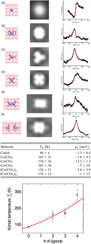 | ||
| Fig. 25 (Top) Models, STM topographies, and STS spectra in the center of the Co adatoms and complexes under investigation: (a) cobalt adatom, (b) Co(CO)2 (constantly flipping; from the spectrum a linear background has been removed), (c) Co(CO)3, (d) Co(CO)4, (e) (Co(CO)2)2, (f) (Co(CO)3)2. Models and topographies in (a)–(f) drawn to the same scale. The solid lines in the spectra are fits of a Fano function, with the parameters determined in the table (middle), where TK is the Kondo temperature and is proportional to the width of the resonances. (bottom) The scaling behavior of a cobalt impurity with nCO molecules attached to it. Data for dicobalt carbonyls are shown as crosses, the number of ligands refers to the number of CO molecules per cobalt atom. Reprinted with permission from ref. 272. Copyright 2005 the American Physical Society. | ||
 | ||
| Fig. 26 Kondo temperature tuning. (a) A sequence of STM images of different number of nearest neighbors (nn) molecules created by removing one molecule at a time with the STM tip (left) from the hexagon and corresponding models (middle). The calculated electron standing wave patterns reveal a gradual exposing of the center molecule (indicated with a red circle) to the surface state electrons. Here white and black colors in the calculated images represent higher and lower electron densities, respectively. The black region under the molecular clusters indicates a reduction of surface electronic charge density. (b) The dI = dVspectra are measured at each step by positioning the tip above the center molecule (indicated with red dot). The spectra are vertically and horizontally displaced for clarity. Horizontal displacements of 3 to 10 meV are taken for the spectra representing nn6, nn5, nn4, nn2, and nn1. (c) The plot of Kondo temperature as a function of the number of nearest neighbors. Reprinted with permission from ref. 273. Copyright 2006 the American Physical Society. | ||
But Kondo resonance has not only been studied in metal–organic systems containing magnetic ions, but also in pure charge-transfer organic assemblies containing a localized unpaired electron.277 Recently, the group of Yamashita extended the investigations of STM and STS to the double-decker SMMs LnPc2 with Ln = Tb(III) and Dy(III) and the isomorphous non-SMM YPc2, adsorbed on an Au(111) surface by thermal evaporation in ultrahigh vacuum (Fig. 27).113,275STM topography images together with conductance mapping of the molecules allow a distinction of the structure of the different LnPc2 lying on the surface, together with the presence of the corresponding LnPc compounds. Still, Kondo effect was only observed for the TbPc compound, the absence of the Kondo effect in the other compounds being related with the temperature of the sample and the interplay of TK with TB (blocking temperature of the SMM). On the other hand, spin coupling through a molecular linker (ligand-mediated exchange coupling) has also been studied for the V2(TCNE) nanostructure by studying the Kondo effect over this system composed by two V atoms connected to a single TCNE ligand.278 It is observed that a strong ferromagnetic coupling between both spins mediated by the TCNE molecule suppresses the Kondo resonance, evidencing the sensibility of this effect to the coupling of the local magnetic moments with the environment. Even though this technique is not optimal for a quantitative measurement of the spin,279 it does give direct evidence of the presence of a net spin in the molecule and of its degree of interaction with the conducting electrons.
 | ||
| Fig. 27 (a) Topographic image, (b) the conductance mapping at V = −0.8 eV and (c) STS of the TbPc molecule. In the plot of STS, the data obtained on the bare Au substrate are superimposed. High resolution STS spectra of (d) and (e) TbPc, (f) DyPc, and (g) YPc. The dI/dV data were obtained using the lock-in amplifier with a modulation voltage of 4 mV. All were obtained by placing the tip at the center of the molecules. (e) Fitting of the spectrum of TbPc with a Fano-shaped function. The smooth red curve is the result of the best fitting. Reprinted with permission from ref. 275. Copyright 2010 The Royal Society of Chemistry. | ||
Current imaging tunnelling spectroscopy. The combination of the spatial resolution given by STM with the resolution of electronic states given by STS results in a powerful technique called current-imaging tunnelling spectroscopy (CITS), which leads to energy resolved conductance maps.220 These maps represent a spatially resolved electron density of states (DOS), that is, a measure of the conductance level (dI/dV) or DOS at a constant energy in all positions of the x–y plane. This can be achieved by measuring the dI/dV signal together with the topographic image measured at a constant tunnelling current I, resulting in a set of data dI/dV(V,x,y). Energy resolved conductance maps are particularly useful for the localization of the positions of metal centres incorporated into an assembly of organic ligands via coordination bonds, due to the energy-selective mapping of the local density of states. They also apply for the identification of the orbital character of the different sated in the DOS. Following the analysis of energy resolved conductance maps, it has been proved that the molecular and electronic structures of different types of molecular magnets are preserved when adsorbed on surfaces. Since some of them show SMM behaviour, it has been inferred that these molecules should also preserve this property on the basis of their isostructural conformation on surfaces, even though no direct evidence of the SMM behaviour is observed using this technique.
One of the first examples of molecular magnets studied by STM and STS techniques are the double decker TbPc2 molecules that show SMM behaviour in bulk. The first measurements of surface-supported TbPc2 single molecules were reported by the group of K. Kern.114 They describe their structural, magnetic and electronic properties by combining STM and STS with numerical simulations based on DFT (Fig. 28). In this case, the molecules were deposited on the surface in UHV conditions using a dry imprint technique (Fig. 6); direct deposition of single molecules as well as clusters was performed through gentle contact of a fibreglass bundle coated with TbPc2 powder with the Cu(111) surface. From energy resolved conductance measurements, they confirm that the molecular structure, specifically the Tb-4f electron states, responsible for the large magnetic moment of this molecular magnet, are little affected by the molecular adsorption on the metal surface, and thus it should be expected that TbPc2 molecules adsorbed on a surface preserve their SMM character. Moreover they predict that even in the case of artificially strong metal–molecular interaction such as bond formation between the TbPc2 molecule and the Cu(111) surface, the SMM behaviour of the TbPc2 molecule could still be preserved.
 | ||
| Fig. 28 Energy resolved conductance maps of the TbPc2 molecule deposited on a Cu surface as shown in Fig. 6, at energies A = −0.8 eV, B = 0.4 eV, and C = 0.8 eV. (a) Experimentally measured and (b) calculated energy-resolved charge densities. Reprinted with permission from ref. 114. Copyright 2008 American Chemical Society. | ||
On the other hand, Petukhov et al.220 applied this technique to study the structure of Co [2 × 2] molecular grid and the star-like [FeIII(FeIII(L3)2)3](3·4CHCl3) adsorbed on HOPG and deposited by drop casting. Even these molecules are not strictly SMMs, it is worth to mention these examples because of the interesting results obtained, specifically with submolecular resolution at room temperature, being able to obtain direct information about the positions of individual magnetic ions (its application to large molecules is rather difficult at ambient conditions because of mobility or instability of the molecules, and requires the use of a low-drift STM head).220 In these systems, the density of states near the Fermi level is dominated by the weakly hybridized metal d states, thus allowing the selective mapping of the metal–ion positions, undisturbed by the surrounding organic ligands. Then, by energy-selective mapping of the local density of states, they obtained information for the localization of the positions of the transition-metal centres incorporated into an assembly of organic ligands via coordination bonds. Even the estimated dimensions of the Co [2 × 2] grid and the star-like [FeIII(FeIII(L3)2)3](3·4CHCl3) on HOPG are in perfect agreement with those obtained by X-ray crystallography, again no direct information on the magnetization properties of the molecule is obtained in this way. This technique has also been applied to probe the deposition of a Co(II) cubane [CoII4(Cl)4(HL)4] SMM on HOPG surfaces in a dichloromethane solution with very low concentration.280 In this case, the resolution is very poor due to CITS measurements at room temperature and under atmospheric pressure.
Albeit this technique neither allows for a quantitative determination of magnetic properties as previously described for scanning tunnelling spectroscopy, it is useful to characterize the molecular structure of the system once deposited on the surface. From this analysis, it is possible to infer the surface effects on the magnetic properties of the molecule.
Inelastic electron tunnelling spectroscopy or spin-flip spectroscopy. One of the first STM based techniques allowing for direct determination of the magnetic properties of a system is based on the analysis of the second derivative of the tunnelling current versus tip-sample bias, and called Inelastic Electron Tunnelling Spectroscopy (IETS). It takes into account the additional current contribution to the tunnelling current generated by inelastic processes by which some of the tunnelling electrons lose their energy by exciting vibrations of the adsorbate. With increasing bias voltage one observes a conductance step (step in the dI/dVspectra) each time the tunnelling electrons reach the threshold energy needed to excite one new vibration of the system, opening a new inelastic conductance channel. Still, the inelastic contribution to the current is small compared to the elastic tunnelling current (∼0.1%) and thus is more clearly seen as a peak in the second derivative of the current to the bias voltage. So peaks in this measurement give information on the vibrations of the adsorbate. In this regard, Heinrich and co-workers at the low-T STM lab founded by D. Eigler at IBM Almaden have pioneered spin excitation spectroscopy as a tool to quantify the magnetic properties of individual atoms or clusters.281,282 The technique IETS measures inelastic couplings of several kinds, such as excitation energies of vibrations,281 changes in the magnetic state of atoms or molecules,282 as well as surface magnons283 by the conductivity of the tunnel junction. For magnetic atoms, the energies and amplitudes of the conductance steps observed in the second derivative of the current to bias voltage correspond to spin excitations, where the tunnelling electrons transfer energy to the spin degree of freedom of the system. They deliver valuable information on the magnetic ground state and anisotropy of magnetic atoms,284 and in the case of clusters also on the Heisenberg exchange coupling between the atoms in the cluster.285–287 In this way, quantitative information on the magnetic quantum states of single atoms adsorbed onto surfaces, such as magnetic anisotropy and magnetic exchange coupling energies can be deduced with spin excitation spectroscopy.247,288
Although STM is capable of atomic resolution and can be a sensor for atomic magnetism when imaging solid surfaces, mapping of large and complex molecules with submolecular resolution still remains a difficult task, especially for organic molecules because of their mobility and instability. Beyond these limitations, some recent examples have already shown the ability of spin-flip spectroscopy to probe superexchange interaction in thin films of CoPc molecular magnets.285,287 Ordered multilayer structures of CoPc were obtained by sublimation of CoPc molecules onto Pb islands at room temperature to form a SAM with square lattice pattern, and subsequent sublimation at 120 K to form the ordered multilayer (Fig. 29). The absence of Kondo resonance for the molecules directly adsorbed on the Pb surface indicated the spin quenching for the first layer of CoPc molecules, which served as an insulating buffer to prevent the spins above it from being quenched by the Pb metallic substrate. Spin excitations of the chain-like stacks formed by the CoPc molecules from the second to the fifth layer are observed, that can be well described by the Heisenberg Hamiltonian corresponding to a chain of N molecules antiferromagnetically coupled. This observed antiferromagnetic ordering of the molecular chain is a result of the superexchange interaction among the CoPc units of different layers, while the interchain interaction dominated by noncovalent binding forces among CoPc units in the same layer has negligible effect on the magnetic coupling.
 | ||
| Fig. 29 CoPc multilayers on Pb. (a) STM image (V = 0.9 V, I = 0.03 nA) of the self-assembled multilayers of CoPc molecules on Pb(111) film (26 layers thick). (b) Molecular structure of CoPc. (c) STM image (V = 0.6 V, I = 0.1 A) showing the relative stacking of the 1st and 2nd CoPc layers. (d) STM image showing the relative stacking of the 2nd and 3rd CoPc layers. The white and black dots indicate the centers of the molecules on the 2nd and 3rd layers, respectively. (e) Stacking geometry of CoPc molecules. The molecular layers are spaced 3.5 ± 0.1 Å apart. The insets show the orientation and displacement between molecules in adjacent layers. Spin-flip spectra of individual CoPc chains. (f) Spectrum acquired with the STM tip positioned on the third molecular layers. The tunneling gap was set at V = 50 mV, I = 0.2 nA. The bias modulation was 1 mV (rms) at 1991 Hz. The arrows indicate the inelastic tunneling threshold voltages. (g) Spectra on the third layer in different magnetic fields. The STS were acquired at a set point of V = 10 mV and I = 0.15 nA at T = 0.4 K. The arrows indicate the three steps induced by 11 T magnetic field. The lock-in modulation was 0.05 mV at 1991 Hz. (h) Schematic of the spin singlet to triplet transition. The triplet states are labeled by the magnetic quantum number Sz. Sc is the total spin of the chain. Reprinted with permission from ref. 285. Copyright 2008 the American Physical Society. | ||
Zero-field splitting values of Iron(II) phthalocyanines (FePc) were also determined by means of IETS with STM. Tukahara et al. measured the energy splitting generated by spin-orbit coupling in FePc molecules sublimated onto a clean and oxidized Cu(100) surfaces, and its dependence with the applied magnetic field.286,287FePc molecules are characteristic since they take a triplet spin state with S = 1. From the steps observed in the conductance spectra, a negative value for the axial zero field constant D is obtained for the FePc molecules adsorbed on a (2 × 1)-O surface, in contrast to the positive values corresponding to the FePc in bulk. This means that the interaction with the substrate allows turning from the molecule bulk easy plane magnetic anisotropy to the easy axis magnetic anisotropy when the FePc is attached to the substrate. This is achieved by changing the balance between the in-plane and the out-of-plane orbital motions that determine the sign of D and hence the magnetic anisotropy. Indeed, the ZFS disappears when the FePc is placed on a clean Cu(110) substrate, since the strong metallic electronic structure of this surface causes stronger coupling of FePc with the substrate and leads the molecule to a null spin state with S = 0, remarking the crucial importance of the electronic coupling between a molecule and a substrate in order to manipulate its spin state. Again, electronic decoupling with the substrate, and thus survival of the S = 1 state is observed for higher layers of FePc, revealing the buffer behaviour of the first layer of magnetic molecules on metallic surfaces.
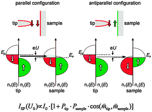 | ||
| Fig. 30 Principle of spin-polarized scanning tunneling microscopy (SP-STM): the spin-polarized tunneling current flowing between a magnetic tip and a magnetic sample depends on the relative alignment of the local magnetization of the tip and sample as well as on the spin polarization of the electronic states of the tip and sample contributing to the tunneling current. Reprinted with permission from ref. 290. Copyright 2009 the American Physical Society. | ||
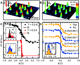 | ||
| Fig. 31 (a) and (b) Topographs of an area with several adatoms colorized with the spin-polarized dI/dV map at B = −0.5 T parallel to the tip magnetization MT (a) and B = +0.5 T antiparallel to MT (b) (T = 0.3 K). (c) Magnetization curves from the same adatom taken at different temperatures as indicated (dots). The insets show the resulting histograms of the fitted magnetic moments (in mB) for the same 11 adatoms at T = 4.2 K (black) and at 0.3 K (red) (top histogram) and for 38 hcp (orange) and 46 fcc (blue) adatoms at 0.3 K (bottom histogram, fcc bars stacked on hcp). (d) Magnetization curves of four adatoms at 0.3 K with fit curves and resulting Bsat of 99% saturation. The inset shows the histogram of Bsat (in T) for the same adatoms used in the lower histogram in (c) (fcc bars stacked on hcp). Curves in (c) and (d) are offset for clarity. Tunneling parameters are as follows: I = 0.8 nA, V = 0.3 V, Vmod = 20 mV. From ref. 296. Reprinted with permission from AAAS. | ||
The development of SP-STM technique was primarily motivated by a combination of the atomic-resolution capability of STM with spin sensitivity, and has been successfully applied to several different classes of materials, achieving the level of resolution of individual magnetic atoms adsorbed on nonmagnetic substrates, to investigate topics such as the coupling of the individual magnetic atoms and molecules to magnetic substrates, or the coupling between two magnetic adatoms mediated by the substrate. Although SP-STM is suitable for adatoms, only very recently similar experiments have been performed on molecules. The SP-STM technique was applied for the first time to a single Co–phthalocyanine (CoPc) molecule,297 adsorbed on a Co nanoisland grown on a Cu(111) substrate (Fig. 32). A different spin current was measured, depending on whether the spin of the CoPc molecule was oriented up or down, demonstrating the feasibility of SP-STM to directly visualize the spin state of a single molecule. In that case, it was proved that the interaction between the CoPc and the substrate was ferromagnetic, and that the organic ligands played an important role in both, the transmission of the ferromagnetic interactions and the adsorption geometry of CoPc. Brede et al. subsequently reported a significant spin-polarization for a CoPc molecule in contact with a ferromagnetic Fe thin film;298 the observed spin polarization is identified as a consequence of the molecule-substrate hybrid states, arising from the local molecule-surface bonding at different parts of the molecule, since a transfer of one electron from the surface to the molecule annihilates the molecular spin. Such a bonding is favoured by the van der Waal forces that play a crucial role by bringing the molecule 0.5 Å closer to the surface. In this regard, it is necessary to keep on the effort to understand the properties of organic/magnetic interfaces, since the creation of complex magnetic structures based on organic systems can lead to tools for the manipulation of local spin-polarization on magnetic surfaces.299
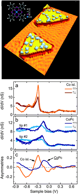 | ||
| Fig. 32 (top) Pseudo-three-dimensional STM image (40 × 20 nm2, 0.1 V, 0.5 nA) of CoPc molecules adsorbed on cobalt nanoislands grown on Cu(111). The spatial oscillations on the Cu(111) surface are due to the scattering of the Shockley surface-state electrons. The inset shows structure model for CoPc (a) typical spin-polarized dI = dV over two cobalt nanoislands of opposite magnetization (noted ↑↑ and ↑↓). Feedback loop opened at 0.6 V and 0.5 nA; (b) differential conductance (dI = dV) over the center of single CoPc molecules adsorbed on cobalt nanoislands of opposite magnetization. Two sets of spectra acquired with distinct tips (noted 1 and 2) are presented. The spectra acquired with tip 1 are displaced upward by 6 nS for clarity. Feedback loop opened at 0.6 V and 0.5 nA. (c) Asymmetries arising from opposite magnetizations for CoPc and the Co nanoislands. The asymmetries are an average of all the recorded asymmetries obtained with different tips. Reprinted with permission from ref. 297. Copyright 2008 the American Physical Society. | ||
Another candidate very promising to be applied for SP-STM studies is the double decker SMM made of a single lanthanide ion sandwiched between two phthalocyanine units (LnPc2). Phthalocyanine units have been identified to play a crucial role in this double decker SMM, and furthermore, the LnPc2 units form 2D arrays on surfaces,50 similar to CoPc molecules, that form perfect 2D networks by spontaneously ordering through lateral hydrogen bonds, when deposited on metals surfaces in ultrahigh vacuum. This means that single units can be identified and addressed by their position on the 2D array.
Even reading the spin of a molecule seems feasible with the SP-STM technique, it is to be stated that no successful writing process (that is, control on the switch of the magnetic moments) has yet been demonstrated for the case of magnetic molecules; at the moment, the only available examples are the exceptional reversal of the magnetization in the Co metal island by SP-STM spin transfer torque,294 and the change in the spin direction of a single Co atom by performing lateral atom manipulation on a magnetic template with a SP-STM.300,301
Up to now, we have reviewed how STM based techniques have been applied to perform different kind of direct and indirect magnetic measurements on different solid state or molecular materials, working with static images. In this sense, Loth et al. have focused their efforts on the application of SP-STM to study dynamic magnetic properties of spins on surfaces such as the electron spin relaxation time with nanosecond time resolution of individual atoms adsorbed on a surface, by using an all-electronic pump-probe measurement scheme.302 This experiment opens the field to apply this atomic spin sensitive technique to monitor the dynamical evolution of the excited state of a system with atomic resolution, such as the vibration of an atom or molecule and even the precession of a spin.
The application of this technique in its actual format was first done by the same author,303 to detect paramagnetic defects in oxidized silicon surfaces, as well as iron islands on Si.306 The effectiveness of this technique has also been tested with organic molecules by various groups who focused their attention on different instrumental setups using well known ESR standards.307 Molecules might have the ability to self-organize on surfaces forming either nanodots or regular monolayers and moreover, preserve its magnetism when dispersed in such surfaces. Some examples are aggregates of commercially available free radicals such as bisdiphenylene-phenylallyl (BDPA),307,3081,1-diphenyl-2-picrylhydrazyl (DPPH),307TEMPO or TEMPOL free radicals.
Mugnani et al. used ESN-STM to address the behaviour of polychlorotriphenylmethyl (PTM) radical derivatives, like the tris(2,4,6-thrichlorophenyl)methyl radical (TTM), at the single molecule level (Fig. 33).222 Samples prepared by the dip and rinse procedure showed TTM molecules adsorbed on the entire gold surface forming ordered structures of a diameter of less than 8 nm. Good ESN-STM spectra and images proved the possibility to use this technique for the detection of single spin centres on the surface, and demonstrated that these molecules retain the paramagnetic character when adsorbed on a surface. More recently, Gorini et al. extended the results of ESN-STM measurements of a thin magnetic film of thiol-functionalized nitronyl-nitroxide radicals chemically bound to a gold surface.309,310 Finally, other SAMs of radical molecules physisorbed on HOPG that retain their paramagnetic behaviour have been assessed as candidates for further single spin detection experiments using ESN-STM.96
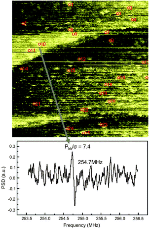 | ||
| Fig. 33 Top: ESN-STM image of TTM dispersed on gold, without any filtering. The sample was prepared by the dip and rinse procedure. While scanning ESN spectra are acquired in correspondence of detected objects, in particular the ESN spectrum presented in the bottom part corresponds to the aggregate number 10. Reprinted from ref. 222, Copyright 2009, with permission from Elsevier Masson SAS. | ||
The current demand of characterization tools at the single molecular level and protocols for spin read out at room temperature impulse this technique to be further developed since it is a promising technique to achieve these strong experimental challenges. Some of the improvements should be addressed to the anchoring of the species to be used in high vacuum to prevent diffusion of the species on the surface and also to extend the technique to low temperatures. Another possible goal could be to use this technique to detect the spin Larmor frequency of SMMs deposited on surfaces.
4.7. Other scanning probe microscopies
There are very few examples of MFM measurements of magnetic molecules or single molecule magnets. One of the main reasons is that the resolution limit, determined strongly by the size of the tip apex, is of the order of few nanometres, and easily exceeds the typical size of molecular clusters. On the other side, the MFM technique is suitable to detect magnetically ordered regions on a surface, and most of molecular magnets are paramagnetic at room temperature, and show ordering temperatures in the range of few K. That requires the use of either low temperatures or high magnetic fields to saturate the magnetic moment of the sample. Finally, the sensitivity of MFM is above the single molecule limit, thus it is generally restricted to the detection of small aggregates rather than isolated molecules.
To the best of our knowledge, the first and single example of MFM magnetic characterization of a SMM was done by Ruiz-Molina et al. on isolated Mn12-biph SMMs on the surface of polymeric thin films.124MFM images were taken at a retrace distance of 30 nm and show the magnetic signal of the corresponding topographic patterning of the SMMs on the surface (Fig. 34).82
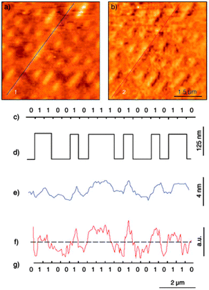 | ||
| Fig. 34 (a) AFM topography image of a DVD replica after solvent exposure (rms roughness is 1 nm). (b) Magnetic mapping of (a) with MFM. The image (phase shift during second pass) was acquired by a two-pass mode using a cobalt-coated magnetic tip. The lift height was 30 nm. (c) Sequence of bits that is represented by the topographic sequence along the track marked by line 1 in (a). (d) Idealized representation of the corresponding topographical line profile of the track in the replica before exposure to solvent. (e) Topographical line profile of the track after exposure to solvent. (f) Magnetic contrast along line 2 in (b). The mean signal line (a) is a guide to the eye. (g) Sequence of magnetic bits extracted from (f), which shows a perfect correspondence with the original sequence in (c). Reprinted with permission from ref. 82. Copyright 2005 Wiley-VCH Verlag GmbH & Co. KGaA. | ||
Almost at the same time, characterization by MFM was done on another molecule based nanostructure: a purely organic high-spin polyradical magnetic dot of poly(1,2-phenylenevinylene) networks bearing 4-substituted phenoxyl radicals with different molecular weights and spin concentrations315 dispersed on a freshly cleaved HOPG surface. The polyradical had the shape of a pseudo-two-dimensionally extended and planar disk, of about 35 nm diameter and 0.6 nm high. The intensity of the magnetic signal was found to be linearly dependent on the spin concentrations, that is the number of unpaired electrons per molecule.316,317 Since the molecules are paramagnetic, and the measurements were done without any applied external magnetic field, the proposed mechanism for the detection of the magnetic signal is an attractive interaction between the ferromagnetic probe and the radical molecule, which is directly magnetized by the probe located close enough to the sample.
More recently, bimodal MFM has been applied for the magnetic characterization of a single isolated superparamagnetic ferritin molecule.318 Garcia and co-workers were able to identify a single magnetic ferritin molecule, and its non-magnetic conjugate, an apoferritin molecule, in air and liquid (Fig. 35). Indeed, they were able to distinguish the organic peptide shell from the magnetic core and isolate in this way the magnetic signal coming from the core. In this case, they fixed the magnetization of the nanoparticles with an applied magnetic field of 80 mT perpendicular to the surface.
 | ||
| Fig. 35 Scheme of bimodal AFM operation to measure simultaneously mechanical and magnetic interactions. (a) The first two cantilever–tip eigenmodes (ω1,ω2) are excited by applying a mechanical force at the cantilever base. Ferritin molecules are imaged in liquid in the presence of an external magnetic field. (b) The amplitude of the first mode is used to generate an image of the topography in exactly the same way as in amplitude-modulation AFM. The phase shift of the second mode φ2 is used to reconstruct the structure of the protein with its mechanical (protein shell) and magnetic (iron oxide core) contributions. (c) Topography image in buffer (pH = 3) of a deposition containing ferritin and apoferritin molecules (A01 = 7 nm, Asp = 6 nm, A02 = 1.1 nm). (d) Bimodal phase shift image of (c). The phase image shows two different structures: ring-like and full nanoparticles. (e) Phase shift cross section of the nanoparticles marked in (c) and (d). (f) Bimodal phase shift image of the iron oxide core, the peptide shell and an image reconstruction of ferritin revealing the mechanical and the magnetic properties. Reprinted by permission from ref. 318. Copyright 2011 IOP Publishing Ltd. | ||
Ghirri et al. have applied SHPM to study the magnetic features of a molecule-based monolayer of the Cs0.7Ni[Cr(CN)6]0.9 Prussian blue analogue (CsNiCr)-PBA, stabilized in the form of nanoparticles with a diameter of <6 nm and selectively deposited on a functionalized Si(100) surface (Fig. 36).38 The magnetic signal of the sample was obtained after scanning over the surface at a height of 350 nm. Analysis of the hysteresis cycles with a field of up to 1 T applied perpendicular to the surface obtained at T = 20 K shows evidence for canted ferromagnetism in the grafted NP ordering.
 | ||
| Fig. 36 (a) Experimental set-up of the SHPM illustrating the disposal of sample, scanning head and magnetic fields. (b) STM image taken at T = 100 K showing the patterning of the surface. (c) Magnetic image taken at T = 100 K simultaneously with (b) and with an applied-field H = +70 kOe. The color scale indicates the strength of the detected stray field. The zero-field value of the scale is set to an arbitrary baseline. (d) Same as (c) but with reversed field (H = −70 kOe): notice that the color scale is reversed while the same spots are observed. Reprinted with permission from ref. 38. Copyright 2008 Wiley-VCH Verlag GmbH & Co. KGaA. | ||
5. Summary
Everybody agrees that the development of magnetic molecular devices, though a breakthrough if successful, nowadays represents a real challenge due to the technological limitations as well as the lack of basic information about the behaviour of the magnetic molecules upon integration. A detailed revision of the main scientific approaches developed over the last 10–12 years to overcome such technological challenges has been given in this review. For this, the manuscript has been divided into the three main areas we consider crucial, and therefore, that require special attention: (I) development of structuration techniques that allow for a proper organization of the molecular materials on surfaces and devices, (II) retrieval of basic information about the chemical stability but mainly about the conservation of their magnetic properties obtained by a wide range of techniques on the translation from the macroscopic to the nanoscopic world, contrasting the results obtained by some of them and (III) integration on sensors and feasibility of their functioning on real devices.As expected, the first area involving the development of surface structuration techniques is where scientists started to develop their work, and consequently, where most examples have been described. Most of the different experimental approaches used with this aim are not specific for molecular materials but have already been applied for nanostructured magnetic materials, embracing from self-assembly to AFM lithographies or different vacuum techniques. However, and in spite of the already large number of techniques described, new examples of techniques continue to appear, trying to full fill the highly requiring demands to build magnetic molecular devices. Though still necessary, from our point of view the scientific community should rather concentrate on the advancement of those techniques more feasible to integrate the molecules on devices rather than simply describe new examples. From all them, those that have been shown to have more potential are self-assembly, vacuum techniques and dip pen nanotechnology (DPN). Remarkable advances have been obtained specially with DPN. Integration of the molecular materials on the most sensitive areas of the sensor has been achieved, allowing for the first direct measurement of ac magnetization molecular submonolayers. Integration of molecules on break-junctions and CNT is also a successful and promising approach to indirectly measure magnetic properties at the single molecule level through conductive measurements.
Though these examples suppose important advances forward on the integration of magnetic molecules on devices, future challenges are still to come. Integration techniques must full fill in the near future also the continuous miniaturization of the devices. Such miniaturization requires not only a major precision on the deposition but also a more careful manipulation, minimizing at all the time the impact over the sensor. When structuration must be achieved over large areas, or under mild conditions, other techniques such as self-assembly arise as the most suitable. However, still a long road is ahead us for this technique to be applicable due to two main limitations, reproducibility and scalability. Improving both limitations will require to have a full control over the self-assembly processes of the molecules, which is not an easy task. Actually, it represents one of the main objectives that pursues molecular nanotechnology nowadays. A good solution to overcome these limitations could be the combination of self-assembly with AFM-assisted lithographies in solution or very precise sputtering techniques if working under vacuum conditions.
If the integration of the molecular materials on the sensors and devices could represent itself a real challenge, the maintenance of the magnetic properties upon integration is a must. Perturbations arising upon molecule–surface interactions can induce numerous changes, from chemical modifications (redox processes, chemical decomposition,…) that completely alter the magnetic properties of the molecule to molecular deformations. Such deformations, though not so drastic as a chemical decomposition, can induce a modification of the magnetic exchange pathway or simply alter the easy-magnetization axes, and therefore, the magnetization relaxation mechanisms and barriers. This is the case of the well-known Mn12 family, which recently was shown to lose its SMM behaviour by XMCD upon surface deposition (special attention is required to not confuse losing the SMM behaviour with favouring the fast relaxation processes upon surface deposition!). On the contrary, other clusters such as that of the Fe4 family or TbPc2 have already been shown to be more compact and resistant, demonstrating that the SMM behaviour features are compatible with surface interactions. In any case, chemical or strength modifications are only observable in the first sML directly in contact with the surface though not to additional layers.
Therefore, one of the first steps that must be followed upon surface integration is the chemical and morphological characterization of the resulting ad-layers. The chemical characterization includes FT-IR, XPS, EELS, TOF-SIMS or other surface-based analytical techniques. Once the chemical stability of the molecules has been confirmed, the next step is the magnetic characterization. When the integration is done into devices, characterization of the resulting hybrid nanodevices can already lead directly or indirectly to the measurement of the magnetic properties of the molecules, but sometimes they are not enough. For this reason, the use of complementary techniques such as XMCD and low-temperature STM techniques are not only required but necessary to extract all the information. Other techniques such as magnetic force microscopy (MFM) have been show to be not reliable when characterizing molecular materials. The low signal coming from these materials can induce several errors even at low temperatures to differentiate them from electrostatic and/or residual topography. Still the surface resolution given by SPM based techniques becomes essential for the future success in the characterisation of magnetic molecular materials structured on surfaces, and thus we believe that different derivatives and further improvements of AFM based techniques will play an important role on the field of molecular magnetism on surfaces.
In summary, though moving on a challenging field that is just starting to see some real applications, the good results obtained over the last few years open new expectations for the possible development of magnetic memories, quantum computing or sensor devices, among others. Surface structuration techniques have shown large advances being therefore necessary to complement in the following years the magnetization characterization techniques. Despite considerable advances, complete and reliable magnetic characterization of SMMs on surfaces still remains as a challenging issue, since the magnetic signal of monolayers, sMLs or single molecules is in most cases still below the limit of conventional characterization techniques. Indeed, techniques with nanometric resolution and very high magnetic sensitivity are needed to perform measurements of isolated SMMs, either directly or through conductance measurements. Future research lines in characterization of SMMs on surfaces will undoubtedly address these problems by opening to a wider range of techniques.
Last but not least, in most of the cases for these applications to become a reality, it would be also certainly necessary to increase the blocking temperature of the SMMs, at least over the nitrogen temperature. Working down to kelvin or even millikelvin can suppose a real limitation for the development of the devices even if technologically feasible. As an alternative for certain applications, such as that of molecular memories, the use of switchable spin-crossover or valence tautomerism could be a valuable alternative.
List of the most important acronyms
| μSR | Muon Spin Rotation |
| 2DEG | Two-Dimensional Electron Gas |
| 4-MMTBA | 4-(Mercaptomethyl)-2,3,5,6-tetrafluorobenzoic acid |
| 4-MOBCA | 4′-Mercaptooctafluorobiphenyl-4-carboxylic acid |
| 4-MTBA | 4-Mercapto-2,3,5,6-tetrafluorobenzoic |
| AFM | Atomic Force Microscopy |
| ATR-IR | Attenuated Total Reflection-Infrared Spectroscopy |
| CITS | Current-Imaging Tunneling Spectroscopy |
| CNT | Carbon Nanotube |
| DFT | Density Functional Theory |
| DPN | Dip-Pen Nanolithography |
| EBL | Electron-Beam Lithography |
| EPR | Electron Paramagnetic Resonance |
| ESD | Electrospray Deposition |
| ESN-STM | Electron Spin Noise Scanning Tunneling Microscopy |
| FDMRS | Frequency Domain Magnetic Resonance Spectroscopy |
| FET | Field Effect Transistors |
| FIB | Focused Ion Beam |
| Hdpm | Dipivaloylmethane |
| HFEPR | High Field Electron Paramagnetic Resonance |
| HOPG | Highly Oriented Pyrolytic Graphite |
| Htmhd | 2,2,6,6-Tetramethylheptane-3,5-dione |
| IETS | Inelastic Electron Tunneling Spectroscopy |
| INS | Inelastic Neutron Scattering |
| LCW | Lithographically Controlled Wetting |
| LDOS | Local Density of Electronic States |
| LE-μSR | Low-Energy Muon Spin Resonance |
| LON | Local Oxidation Nanolithography |
| MAPLE | Matrix Assisted Pulsed Laser Evaporation |
| MCD | Magnetic Circular Dichroism |
| MFM | Magnetic Force Microscopy |
| Mn12-ac | Mn12-acetate |
| Mn12-th | Mn12-thiophene-3-carboxylate |
| MNM | Molecular Nanomagnet |
| MOKE | Magneto Optical Kerr Effect |
| NitR | Nitronyl Nitroxide Radicals |
| NP | Nanoparticle |
| Pc | Phthalocyanine |
| Piv | Pivalate or trimethylacetate |
| PLD | Pulsed Laser Deposition |
| PMMA | Poly(methyl methacrylate) |
| POM | Polyoxometalate |
| PTM | Polychlorotriphenylmethyl |
| RPES | Resonant Photoelectron Spectroscopy |
| SAM | Self-Assembled Monolayer |
| SCO | Spin-Crossover |
| SEM | Scanning Electron Microscopy |
| SET | Single-Electron Transistor |
| SHPM | Scanning Hall Probe Microscopy |
| sML | Sub-Monolayer |
| SMM | Single Molecule Magnet |
| SPM | Scanning Probe Microscopy |
| SP-STM | Spin-Polarized Scanning Tunneling Microscopy |
| SQUID | Superconducting Quantum Interference Device |
| SSQM | Scanning Superconducting Quantum Interference Device Microscopy |
| STM | Scanning Tunneling Microscopy |
| STS | Scanning Tunneling Spectroscopy |
| TbPc2 | Bis(phthalocyaninato) Terbium(III) |
| TEY | Total Electron Yield |
| ToF-SIMS | Time of Flight Secondary Ion Mass Spectroscopy |
| Tpc | 3-Thiophenecarboxylate |
| TTM | Tris(2,4,6-thrichlorophenyl)methyl |
| UHV | Ultra-High Vacuum |
| XAS | X-Ray Absorption Spectroscopy |
| XMCD | X-Ray Magnetic Circular Dichroism |
| XNLD | X-Ray Natural Linear Dichroism |
| XPS | X-Ray Photoelectron Spectroscopy |
| ZFS | Zero Field Splitting |
| β-NMR | β-Detected Nuclear Magnetic Resonance |
| μCP | Microcontact Printing |
Acknowledgements
This work was supported by project MAT2009-13977-C03. N.D. and E.B. thank the Ministerio de Ciencia e Innovación for respective JdC and FPI-phD contracts. Authors acknowledge useful discussions with A. Mugarza.References
- Magnetochemistry, ed. R. D. L. Carlin, Springer-Verlag, Berlin, 1986 Search PubMed.
- Magneto-structural Correlations in Exchange Coupled Systems, ed. R. D. Willet, D. Gatteschi and O. Kahn, Reidel Publishing, Dordrecht, The Netherlands, 1983 Search PubMed.
- Molecular Magnetism, ed. O. Kahn, VCH, Weinheim, Germany, 1993 Search PubMed.
- Molecular Nanomagnets, ed. D. Gatteschi, R. Sessoli and J. Villain, Oxford University Press, Oxford, UK, 2006 Search PubMed.
- D. Maspoch, N. Domingo, D. Ruiz-Molina, K. Wurst, J. Tejada, C. Rovira and J. Veciana, J. Am. Chem. Soc., 2004, 126, 730–731 CrossRef CAS.
- D. Maspoch, N. Domingo, D. Ruiz-Molina, K. Wurst, G. Vaughan, J. Tejada, C. Rovira and J. Veciana, Angew. Chem., Int. Ed., 2004, 43, 1828–1832 CrossRef CAS.
- D. Maspoch, N. Domingo, N. Roques, K. Wurst, J. Tejada, C. Rovira, D. Ruiz-Molina and J. Veciana, Chem.–Eur. J., 2007, 13, 8153–8163 CrossRef CAS.
- R. Sessoli, D. Gatteschi, A. Caneschi and M. A. Novak, Nature, 1993, 365, 141–143 CrossRef CAS.
- E. Evangelio and D. Ruiz-Molina, Eur. J. Inorg. Chem., 2005, 2957–2971 CrossRef CAS.
- J. R. Friedman, M. P. Sarachik, J. Tejada and R. Ziolo, Phys. Rev. Lett., 1996, 76, 3830–3833 CrossRef CAS.
- L. Thomas, F. Lionti, R. Ballou, D. Gatteschi, R. Sessoli and B. Barbara, Nature, 1996, 383, 145–147 CrossRef CAS.
- J. M. Hernández, X. X. Zhang, F. Luis, J. Bartolomé, J. Tejada and R. Ziolo, Europhys. Lett., 1996, 35, 301–306 CrossRef CAS.
- D. Maspoch, D. Ruiz-Molina, K. Wurst, N. Domingo, M. Cavallini, F. Biscarini, J. Tejada, C. Rovira and J. Veciana, Nat. Mater., 2003, 2, 190–195 CrossRef CAS.
- F. Prins, M. Monrabal-Capilla, E. A. Osorio, E. Coronado and H. S. J. van der Zant, Adv. Mater., 2011, 23, 1545–1549 CrossRef CAS.
- N. Crivillers, M. Mas-Torrent, J. Vidal-Gancedo, J. Veciana and C. Rovira, J. Am. Chem. Soc., 2008, 130, 5499–5506 CrossRef CAS.
- L. Krusin-Elbaum, T. Shibauchi, B. Argyle, L. Gignac and D. Weller, Nature, 2001, 410, 444–446 CrossRef CAS.
- M. Affronte, J. Mater. Chem., 2009, 19, 1731–1737 RSC.
- Macroscopic Quantum Tunneling of the Magnetic Moment, ed. E. M. Chudnovsky and J. Tejada, Cambridge University Press, Cambridge, 1998 Search PubMed.
- E. del Barco, N. Vernier, J. M. Hernandez, J. Tejada, E. M. Chudnovsky, E. Molins and G. Bellessa, Europhys. Lett., 1999, 47, 722–728 CrossRef.
- M. N. Leuenberger and D. Loss, Nature, 2001, 410, 789–793 CrossRef CAS.
- J. Lehmann, A. Gaita-Arino, E. Coronado and D. Loss, J. Mater. Chem., 2009, 19, 1672–1677 RSC.
- J. Camarero and E. Coronado, J. Mater. Chem., 2009, 19, 1678–1684 RSC.
- M. Evangelisti and E. K. Brechin, Dalton Trans., 2010, 39, 4672–4676 RSC.
- R. Shaw, R. H. Laye, L. F. Jones, D. M. Low, C. Talbot-Eeckelaers, Q. Wei, C. J. Milios, S. Teat, M. Helliwell, J. Raftery, M. Evangelisti, M. Affronte, D. Collison, E. K. Brechin and E. J. L. McInnes, Inorg. Chem., 2007, 46, 4968–4978 CrossRef CAS.
- G. Molnár, S. Cobo, J. A. Real, F. Carcenac, E. Daran, C. Vieu and A. Bousseksou, Adv. Mater., 2007, 19, 2163–2167 CrossRef CAS.
- S. Cobo, G. Molnár, J. A. Real and A. Bousseksou, Angew. Chem., Int. Ed., 2006, 45, 5786–5789 CrossRef CAS.
- C. Thibault, G. Molnár, L. Salmon, A. Bousseksou and C. Vieu, Langmuir, 2009, 26, 1557–1560.
- M. Cavallini, I. Bergenti, S. Milita, G. Ruani, I. Salitros, Z.-R. Qu, R. Chandrasekar and M. Ruben, Angew. Chem., Int. Ed., 2008, 47, 8596–8600 CrossRef CAS.
- M. Cavallini, I. Bergenti, S. Milita, J. C. Kengne, D. Gentili, G. Ruani, I. Salitros, V. Meded and M. Ruben, Langmuir, 2011, 27, 4076–4081 Search PubMed.
- M. Mannini, L. Sorace, L. Gorini, F. M. Piras, A. Caneschi, A. Magnani, S. Menichetti and D. Gatteschi, Langmuir, 2007, 23, 2389–2397 CrossRef.
- M. Mannini, D. Rovai, L. Sorace, A. Perl, B. J. Ravoo, D. N. Reinhoudt and A. Caneschi, Inorg. Chim. Acta, 2008, 361, 3525–3528 CrossRef CAS.
- M. Mas-Torrent, N. Crivillers, V. Mugnaini, I. Ratera, C. Rovira and J. Veciana, J. Mater. Chem., 2009, 19, 1691–1695 RSC.
- C. Simão, M. Mas-Torrent, N. Crivillers, V. Lloveras, J. M. Artés, P. Gorostiza, J. Veciana and C. Rovira, Nat. Chem., 2011, 3, 359–364 Search PubMed.
- A. Robin, L. Marnell, J. Bjork, M. S. Dyer, P. S. Bermudez, S. Haq, S. D. Barrett, M. Persson, A. Minoia, R. Lazzaroni and R. Raval, J. Phys. Chem. C, 2009, 113, 13223–13230 CrossRef CAS.
- S. Stepanow, N. Lin and J. V. Barth, J. Phys.: Condens. Matter, 2008, 20, 184002 CrossRef.
- H. Wende, M. Bernien, J. Luo, C. Sorg, N. Ponpandian, J. Kurde, J. Miguel, M. Piantek, X. Xu, P. Eckhold, W. Kuch, K. Baberschke, P. M. Panchmatia, B. Sanyal, P. M. Oppeneer and O. Eriksson, Nat. Mater., 2007, 6, 516–520 CrossRef CAS.
- P. Gambardella, S. Stepanow, A. Dmitriev, J. Honolka, F. M. F. de Groot, M. Lingenfelder, S. S. Gupta, D. D. Sarma, P. Bencok, S. Stanescu, S. Clair, S. Pons, N. Lin, A. P. Seitsonen, H. Brune, J. V. Barth and K. Kern, Nat. Mater., 2009, 8, 189–193 CrossRef CAS.
- A. Ghirri, A. Candini, M. Evangelisti, G. C. Gazzadi, F. Volatron, B. Fleury, L. Catala, C. David, T. Mallah and M. Affronte, Small, 2008, 4, 2240–2246 CrossRef CAS.
- E. Coronado, C. Martí-Gastaldo, J. R. Galán-Mascarós and M. Cavallini, J. Am. Chem. Soc., 2010, 132, 5456–5468 CrossRef CAS.
- B. Fleury, F. Volatron, L. Catala, D. Brinzei, E. Rivière, V. Huc, C. David, F. Miserque, G. Rogez, L. Baraton, S. Palacin and T. Mallah, Inorg. Chem., 2008, 47, 1898–1900 CrossRef CAS.
- D. Gatteschi and R. Sessoli, Angew. Chem., Int. Ed., 2003, 42, 268–297 CrossRef CAS.
- R. Sessoli, H. L. Tsai, A. R. Schake, S. Wang, J. B. Vincent, K. Folting, D. Gatteschi, G. Christou and D. N. Hendrickson, J. Am. Chem. Soc., 1993, 115, 1804–1816 CrossRef CAS.
- M. Clemente-León, H. Soyer, E. Coronado, C. Mingotaud, C. J. Gómez-García and P. Delhaès, Angew. Chem., Int. Ed., 1998, 37, 2842–2845 CrossRef CAS.
- M. Clemente-León, E. Coronado, A. Soriano-Portillo, C. Mingotaud and J. M. Dominguez-Vera, Adv. Colloid Interface Sci., 2005, 116, 193–203 CrossRef CAS.
- N. Domingo, F. Luis, M. Nakano, M. Muntó, J. Gómez, J. Chaboy, N. Ventosa, J. Campo, J. Veciana and D. Ruiz-Molina, Phys. Rev. B: Condens. Matter, 2009, 79, 214404 CrossRef.
- C. Carbonera, I. Imaz, D. Maspoch, D. Ruiz-Molina and F. Luis, Inorg. Chim. Acta, 2008, 361, 3951–3956 Search PubMed.
- D. M. Seo, V. Meenakshi, W. Teizer, H. Zhao and K. R. Dunbar, J. Magn. Magn. Mater., 2006, 301, 31–36 CrossRef CAS.
- G. Otero, E. Evangelio, C. Rogero, L. Vázquez, J. Gómez-Segura, J. A. M. Gago and D. Ruiz-Molina, Langmuir, 2009, 25, 10107–10115 Search PubMed.
- A. Nait, J. P. Bucher, G. Ph, P. Rabu and M. Drillon, Adv. Mater., 2005, 17, 1612–1616 CrossRef CAS.
- J. Gomez-Segura, I. Diez-Perez, N. Ishikawa, M. Nakano, J. Veciana and D. Ruiz-Molina, Chem. Commun., 2006, 2866–2868 RSC.
- A. Cornia, C. F. Antonio, P. Mirko, Z. Laura, B. Daniele, C. Andrea, G. Dante, B. Roberto, P. Umberto Del, R. Valentina De, G. Leonid and S. J. V. d. Z. Herre, Angew. Chem., Int. Ed., 2003, 42, 1645–1648 CrossRef CAS.
- A. Cornia, A. C. Fabretti, M. Pacchioni, L. Zobbi, D. Bonacchi, A. Caneschi, D. Gatteschi, R. Biagi, U. del Pennino, V. De Renzi, L. Gurevich and H. S. J. Van der Zant, J. Magn. Magn. Mater., 2004, 272–276, E725–E726 Search PubMed.
- L. Zobbi, M. Mannini, M. Pacchioni, G. Chastanet, D. Bonacchi, C. Zanardi, R. Biagi, U. del Pennino, D. Gatteschi, A. Cornia and R. Sessoli, Chem. Commun., 2005, 1640–1642 RSC.
- F. Pineider, M. Mannini, R. Sessoli, A. Caneschi, D. Barreca, L. Armelao, A. Cornia, E. Tondello and D. Gatteschi, Langmuir, 2007, 23, 11836–11843 CrossRef CAS.
- F. Moro, V. Corradini, M. Evangelisti, V. De Renzi, R. Biagi, U. del Pennino, C. J. Milios, L. F. Jones and E. K. Brechin, J. Phys. Chem. B, 2008, 112, 9729–9735 CrossRef CAS.
- U. del Pennino, V. Corradini, R. Biagi, V. De Renzi, F. Moro, D. W. Boukhvalov, G. Panaccione, M. Hochstrasser, C. Carbone, C. J. Milios and E. K. Brechin, Phys. Rev. B: Condens. Matter, 2008, 77, 085419 CrossRef.
- A.-L. Barra, F. Bianchi, A. Caneschi, A. Cornia, D. Gatteschi, L. Gorini, L. Gregoli, M. Maffini, F. Parenti, R. Sessoli, L. Sorace and A. M. Talarico, Eur. J. Inorg. Chem., 2007, 4145–4152 CrossRef CAS.
- M. Mannini, F. Pineider, P. Sainctavit, C. Danieli, E. Otero, C. Sciancalepore, A. M. Talarico, M.-A. Arrio, A. Cornia, D. Gatteschi and R. Sessoli, Nat. Mater., 2009, 8, 194–197 CrossRef CAS.
- D. Gatteschi, A. Cornia, M. Mannini and R. Sessoli, Inorg. Chem., 2009, 48, 3408–3419 CrossRef CAS.
- F. Pineider, M. Mannini, C. Danieli, L. Armelao, F. M. Piras, A. Magnani, A. Cornia and R. Sessoli, J. Mater. Chem., 2010, 20, 187–194 RSC.
- M. J. Rodriguez-Douton, M. Mannini, L. Armelao, A.-L. Barra, E. Tancini, R. Sessoli and A. Cornia, Chem. Commun., 2011, 47, 1467–1469 RSC.
- G. A. Timco, S. Carretta, F. Troiani, F. Tuna, R. J. Pritchard, C. A. Muryn, E. J. L. McInnes, A. Ghirri, A. Candini, P. Santini, G. Amoretti, M. Affronte and R. E. P. Winpenny, Nat. Nanotechnol., 2009, 4, 173–178 CrossRef CAS.
- F. Troiani, M. Affronte, S. Carretta, P. Santini and G. Amoretti, Phys. Rev. Lett., 2005, 94, 190501 CrossRef.
- V. Corradini, F. Moro, R. Biagi, V. De Renzi, U. del Pennino, V. Bellini, S. Carretta, P. Santini, V. A. Milway, G. Timco, R. E. P. Winpenny and M. Affronte, Phys. Rev. B: Condens. Matter, 2009, 79, 144419 CrossRef.
- V. Corradini, A. Ghirri, U. del Pennino, R. Biagi, V. A. Milway, G. Timco, F. Tuna, R. E. P. Winpenny and M. Affronte, Dalton Trans., 2010, 39, 4928–4936 RSC.
- M. Lopes, A. Candini, M. Urdampilleta, A. Reserbat-Plantey, V. Bellini, S. Klyatskaya, L. t. Marty, M. Ruben, M. Affronte, W. Wernsdorfer and N. Bendiab, ACS Nano, 2010, 4, 7531–7537 CrossRef CAS.
- A. Nait, J. P. Bucher, P. Rabu, O. Toulemonde, M. Drillon and P. Gerbier, J. Appl. Phys., 2004, 95, 7345–7347 CrossRef CAS.
- S. Voss, S. Herr, M. Fonin, U. Rudiger, M. Burgert and U. Groth, J. Appl. Phys., 2008, 103, 07B901 Search PubMed.
- M. Burgert, S. Voss, S. Herr, M. Fonin, U. Groth and U. Rudiger, J. Am. Chem. Soc., 2007, 129, 14362–14366 CrossRef CAS.
- S. Voss, O. Zander, M. Fonin, U. Rüdiger, M. Burgert and U. Groth, Phys. Rev. B: Condens. Matter, 2008, 78, 155403 Search PubMed.
- S. Voss, M. Fonin, U. Rüdiger, M. Burgert, U. Groth and Y. S. Dedkov, Phys. Rev. B: Condens. Matter, 2007, 75, 045102 CrossRef.
- G. Condorelli, A. Motta, I. L. Fragalà, F. Giannazzo, V. Raineri, A. Caneschi and D. Gatteschi, Angew. Chem., Int. Ed., 2004, 43, 4081–4084 CrossRef CAS.
- J. S. Steckel, N. S. Persky, C. R. Martinez, C. L. Barnes, E. A. Fry, J. Kulkarni, J. D. Burgess, R. B. Pacheco and S. L. Stoll, Nano Lett., 2004, 4, 399–402 CrossRef CAS.
- G. Condorelli, A. Motta, M. Favazza, P. Nativo, I. L. Fragalà and D. Gatteschi, Chem.–Eur. J., 2006, 12, 3558–3566 CrossRef CAS.
- E. Coronado, A. Forment-Aliaga, F. M. Romero, V. Corradini, R. Biagi, V. De Renzi, A. Gambardella and U. del Pennino, Inorg. Chem., 2005, 44, 7693–7695 CrossRef CAS.
- A. Ghirri, V. Corradini, C. Cervetti, A. Candini, U. del Pennino, G. Timco, R. J. Pritchard, C. A. Muryn, R. E. P. Winpenny and M. Affronte, Adv. Funct. Mater., 2009, 20, 1552–1560 Search PubMed.
- J. Gomez-Segura, O. Kazakova, J. Davies, P. Josephs-Franks, J. Veciana and D. Ruiz-Molina, Chem. Commun., 2005, 5615–5617 RSC.
- H. Sun, W. Li, L. Wollenberg, B. Li, L. Wu, F. Li and L. Xu, J. Phys. Chem. B, 2009, 113, 14674–14680 CrossRef CAS.
- M. Mannini, D. Bonacchi, L. Zobbi, F. M. Piras, E. A. Speets, A. Caneschi, A. Cornia, A. Magnani, B. J. Ravoo, D. N. Reinhoudt, R. Sessoli and D. Gatteschi, Nano Lett., 2005, 5, 1435–1438 CrossRef CAS.
- M. Cavallini, F. Biscarini, J. Gomez-Segura, D. Ruiz and J. Veciana, Nano Lett., 2003, 3, 1527–1530 CrossRef CAS.
- M. Cavallini, J. Gomez-Segura, C. Albonetti, D. Ruiz-Molina, J. Veciana and F. Biscarini, J. Phys. Chem. B, 2006, 110, 11607–11610 CrossRef CAS.
- M. Cavallini, J. Gomez-Segura, D. Ruiz-Molina, M. Massi, C. Albonetti, C. Rovira, J. Veciana and F. Biscarini, Angew. Chem., Int. Ed., 2005, 44, 888–892 CrossRef CAS.
- K. Kim, D. M. Seo, J. Means, V. Meenakshi, W. Teizer, H. Zhao and K. R. Dunbar, Appl. Phys. Lett., 2004, 85, 3872–3874 CrossRef CAS.
- V. Corradini, U. del Pennino, R. Biagi, V. De Renzi, A. Gambardella, G. C. Gazzadi, A. Candini, L. Zobbi and A. Cornia, Surf. Sci., 2007, 601, 2618–2622 CrossRef CAS.
- M. Pacchioni, A. Cornia, A. C. Fabretti, L. Zobbi, D. Bonacchi, A. Caneschi, G. Chastanet, D. Gatteschi and R. Sessoli, Chem. Commun., 2004, 2604–2605 RSC.
- K. Kim, A. Ford, V. Meenakshi, W. Teizer, H. Zhao and K. R. Dunbar, J. Appl. Phys., 2007, 102, 094306 Search PubMed.
- R. V. Martínez, F. García, R. García, E. Coronado, A. Forment-Aliaga, F. M. Romero and S. Tatay, Adv. Mater., 2007, 19, 291–295 CrossRef CAS.
- R. V. Martínez, J. Martínez, M. Chiesa, R. Garcia, E. Coronado, E. Pinilla Cienfuegos and S. Tatay, Adv. Mater., 2010, 22, 588–591 CrossRef CAS.
- B. Basnar and I. Willner, Small, 2009, 5, 28–44 CrossRef CAS.
- K. Salaita, Y. Wang and C. A. Mirkin, Nat. Nanotechnol., 2007, 2, 145–155 CrossRef CAS.
- D. S. Ginger, H. Zhang and C. A. Mirkin, Angew. Chem., Int. Ed., 2004, 43, 30–45 CrossRef.
- E. Bellido, R. d. Miguel, J. Sesé, D. Ruiz-Molina, A. Lostao and D. Maspoch, Scanning, 2010, 32, 35–41 Search PubMed.
- E. Bellido, R. d. Miguel, D. Ruiz-Molina, A. Lostao and D. Maspoch, Adv. Mater., 2010, 22, 352–355 Search PubMed.
- J. P. Cleuziou, W. Wernsdorfer, V. Bouchiat, T. Ondarcuhu and M. Monthioux, Nat. Nanotechnol., 2006, 1, 53–59 CrossRef CAS.
- R. Singh, T. Premkumar, J.-Y. Shin and K. E. Geckeler, Chem.–Eur. J., 2010, 16, 1728–1743 Search PubMed.
- P. Krukowski, Z. Klusek, W. Olejniczak, R. Klepaczko, M. Puchalski, P. Dabrowski, P. J. Kowalczyk and K. Gwozdzinski, Appl. Surf. Sci., 2009, 255, 8769–8773 Search PubMed.
- D. Shi, Y. Guo, Z. Dong, J. Lian, W. Wang, G. Liu, L. Wang and R. C. Ewing, Adv. Mater., 2007, 19, 4033–4037 CrossRef CAS.
- V. Georgakilas, D. Gournis, V. Tzitzios, L. Pasquato, D. M. Guldi and M. Prato, J. Mater. Chem., 2007, 17, 2679–2694 RSC.
- D. A. Britz and A. N. Khlobystov, Chem. Soc. Rev., 2006, 35, 637–659 RSC.
- Y.-L. Zhao and J. F. Stoddart, Acc. Chem. Res., 2009, 42, 1161–1171 CrossRef CAS.
- L. Bogani, C. Danieli, E. Biavardi, N. Bendiab, A.-L. Barra, E. Dalcanale, W. Wernsdorfer and A. Cornia, Angew. Chem., Int. Ed., 2009, 48, 746–750 CrossRef CAS.
- L. Bogani, R. Maurand, L. Marty, C. Sangregorio, C. Altavilla and W. Wernsdorfer, J. Mater. Chem., 2010, 20, 2099–2107 RSC.
- A. Giusti, G. Charron, S. Mazerat, J.-D. Compain, P. Mialane, A. Dolbecq, E. Rivière, W. Wernsdorfer, R. Ngo Biboum, B. Keita, L. Nadjo, A. Filoramo, J.-P. Bourgoin and T. Mallah, Angew. Chem., Int. Ed., 2009, 48, 4949–4952 CrossRef CAS.
- G. Charron, A. Giusti, S. Mazerat, P. Mialane, A. Gloter, F. Miserque, B. Keita, L. Nadjo, A. Filoramo, E. Riviere, W. Wernsdorfer, V. Huc, J. P. Bourgoin and T. Mallah, Nanoscale, 2010, 2, 139–144 RSC.
- S. Kyatskaya, J. R. Galan-Mascaros, L. Bogani, F. Hennrich, M. Kappes, W. Wernsdorfer and M. Ruben, J. Am. Chem. Soc., 2009, 131, 15143–15151 CrossRef CAS.
- J. Means, V. Meenakshi, R. V. A. Srivastava, W. Teizer, A. A. Kolomenskii, H. A. Schuessler, H. Zhao and K. R. Dunbar, J. Magn. Magn. Mater., 2004, 284, 215–219 CrossRef CAS.
- V. Meenakshi, W. Teizer, D. G. Naugle, H. Zhao and K. R. Dunbar, Solid State Commun., 2004, 132, 471–476 CrossRef CAS.
- M. Pervolaraki, G. I. Athanasopoulos, J. Giapintzakis, C. Kizas, A. J. Tasiopoulos, F. Sima, G. Socol and I. N. Mihailescu, J. Optoelectron. Adv. Mater., 2010, 12, 557–560 Search PubMed.
- L. Margheriti, M. Mannini, L. Sorace, L. Gorini, D. Gatteschi, A. Caneschi, D. Chiappe, R. Moroni, F. B. d. Mongeot, A. Cornia, F. M. Piras, A. Magnani and R. Sessoli, Small, 2009, 5, 1460–1466 CrossRef CAS.
- R. Moroni, R. Buzio, A. Chincarini, U. Valbusa, F. B. d. Mongeot, L. Bogani, A. Caneschi, R. Sessoli, L. Cavigli and M. Gurioli, J. Mater. Chem., 2008, 18, 109–115 RSC.
- A. Saywell, G. Magnano, C. J. Satterley, L. M. A. Perdigó, A. J. Britton, N. Taleb, M. del Carmen Giménez-López, N. R. Champness, J. N. O'Shea and P. H. Beton, Nat. Commun., 2010, 1, 75 Search PubMed.
- A. Saywell, A. J. Britton, N. Taleb, M. del Carmen Giménez-López, N. R. Champness, P. H. Beton and J. N. O'Shea, Nanotechnology, 2011, 22, 075704 CrossRef.
- K. Katoh, Y. Yoshida, M. Yamashita, H. Miyasaka, B. K. Breedlove, T. Kajiwara, S. Takaishi, N. Ishikawa, H. Isshiki, Y. F. Zhang, T. Komeda, M. Yamagishi and J. Takeya, J. Am. Chem. Soc., 2009, 131, 9967–9976 CrossRef CAS.
- L. Vitali, S. Fabris, A. M. Conte, S. Brink, M. Ruben, S. Baroni and K. Kern, Nano Lett., 2008, 8, 3364–3368 CrossRef CAS.
- S. Stepanow, J. Honolka, P. Gambardella, L. Vitali, N. Abdurakhmanova, T.-C. Tseng, S. Rauschenbach, S. L. Tait, V. Sessi, S. Klyatskaya, M. Ruben and K. Kern, J. Am. Chem. Soc., 2010, 132, 11900–11901 CrossRef CAS.
- C. Carbone, S. Gardonio, P. Moras, S. Lounis, M. Heide, G. Bihlmayer, N. Atodiresei, P. H. Dederichs, S. Blügel, S. Vlaic, A. Lehnert, S. Ouazi, S. Rusponi, H. Brune, J. Honolka, A. Enders, K. Kern, S. Stepanow, C. Krull, T. Balashov, A. Mugarza and P. Gambardella, Adv. Funct. Mater., 2011, 21, 1212–1228 Search PubMed.
- T. Coradin, J. Larionova, A. A. Smith, G. Rogez, R. Clérac, C. Guérin, G. Blondin, R. E. P. Winpenny, C. Sanchez and T. Mallah, Adv. Mater., 2002, 14, 896–898 CrossRef CAS.
- L. Johnson and J. Matisons, J. Mater. Sci., 2009, 44, 2805–2813 Search PubMed.
- F. Palacio, P. Oliete, U. Schubert, I. Mijatovic, N. Husing and H. Peterlik, J. Mater. Chem., 2004, 14, 1873–1878 RSC.
- J. M. North, T. J. Manning, J. Purcell, J. A. Nienow, E. Olsen, N. S. Dalal, K. Riddle and J. Ekman, Carbon, 2004, 42, 199–203 Search PubMed.
- T. J. Manning, J. Nanosci. Nanotechnol., 2005, 5, 167–174 Search PubMed.
- J. Gomez-Segura, J. Veciana and D. Ruiz-Molina, Chem. Commun., 2007, 3699–3707 RSC.
- E. Coronado, C. Martí-Gastaldo and S. Tatay, Appl. Surf. Sci., 2007, 254, 225–235 CrossRef CAS.
- D. Ruiz-Molina, M. Mas-Torrent, J. Gómez, A. I. Balana, N. Domingo, J. Tejada, M. T. Martínez, C. Rovira and J. Veciana, Adv. Mater., 2003, 15, 42–45 CAS.
- H. J. Bolink, E. Coronado, A. Forment-Aliaga and C. J. Gómez-García, Adv. Mater., 2005, 17, 1018–1023 CrossRef CAS.
- H. J. Bolink, L. Cappelli, E. Coronado and I. Recalde, Adv. Mater., 2006, 18, 920–923 CrossRef CAS.
- M. Mannini, F. Pineider, C. Danieli, F. Totti, L. Sorace, P. Sainctavit, M. A. Arrio, E. Otero, L. Joly, J. C. Cezar, A. Cornia and R. Sessoli, Nature, 2010, 468, 417–421 CrossRef CAS.
- M. Soler, P. Artus, K. Folting, J. C. Huffman, D. N. Hendrickson and G. Christou, Inorg. Chem., 2001, 40, 4902–4912 CrossRef CAS.
- P. Artus, C. Boskovic, J. Yoo, W. E. Streib, L.-C. Brunel, D. N. Hendrickson and G. Christou, Inorg. Chem., 2001, 40, 4199–4210 CrossRef CAS.
- N. E. Chakov, W. Wernsdorfer, K. A. Abboud, D. N. Hendrickson and G. Christou, Dalton Trans., 2003, 2243–2248 RSC.
- B. Fleury, L. Catala, V. Huc, C. David, W. Z. Zhong, P. Jegou, L. Baraton, S. Palacin, P.-A. Albouy and T. Mallah, Chem. Commun., 2005, 2020–2022 RSC.
- B. Fleury, V. Huc, L. Catala, P. Jegou, L. Baraton, C. David, S. Palacin and T. Mallah, CrystEngComm, 2009, 11, 2192–2197 RSC.
- M. Fonin, S. Voss, S. Herr, G. de Loubens, A. D. Kent, M. Burgert, U. Groth and U. Rüdiger, Polyhedron, 2009, 28, 1977–1981 CrossRef CAS.
- G. G. Condorelli, A. Motta, G. Pellegrino, A. Cornia, L. Gorini, I. L. FragalÃ, C. Sangregorio and L. Sorace, Chem. Mater., 2008, 20, 2405–2411 CrossRef CAS.
- G. Pellegrino, A. Motta, A. Cornia, I. Spitaleri, I. L. Fragalà and G. G. Condorelli, Polyhedron, 2009, 28, 1758–1763 CrossRef CAS.
- C. P. Foley and H. Hilgenkamp, Supercond. Sci. Technol., 2009, 22, 064001 Search PubMed.
- W. Wernsdorfer, Supercond. Sci. Technol., 2009, 22, 064013 CrossRef.
- M. B. Ketchen, T. Kopley and H. Ling, Appl. Phys. Lett., 1984, 44, 1008–1010 Search PubMed.
- C. I. Pakes, P. W. Josephs-Franks, R. P. Reed, S. G. Corner and M. S. Colclough, IEEE Trans. Instrum. Meas., 2001, 50, 310–313 CrossRef.
- J. Gallop, P. W. Josephs-Franks, J. Davies, L. Hao and J. Macfarlane, Physica C, 2002, 368, 109–113 Search PubMed.
- W. Wernsdorfer, K. Hasselbach, D. Mailly, B. Barbara, A. Benoit, L. Thomas and G. Suran, J. Magn. Magn. Mater., 1995, 145, 33–39 CrossRef CAS.
- W. Wernsdorfer, D. Mailly and A. Benoit, J. Appl. Phys., 2000, 87, 5094–5096 Search PubMed.
- M. Jamet, W. Wernsdorfer, C. Thirion, D. Mailly, V. Dupuis, P. Mélinon and A. Pérez, Phys. Rev. Lett., 2001, 86, 4676–4679 CrossRef CAS.
- W. Wernsdorfer, E. B. Orozco, K. Hasselbach, A. Benoit, B. Barbara, N. Demoncy, A. Loiseau, H. Pascard and D. Mailly, Phys. Rev. Lett., 1997, 78, 1791–1794 CrossRef CAS.
- S. Bertram, T. Unto, I. K. Esko, M. Michel, R. Leif, P. Mikko, W. Wolfgang and B. Alain, Appl. Organomet. Chem., 1998, 12, 315–320 Search PubMed.
- W. Wernsdorfer, B. Doudin, D. Mailly, K. Hasselbach, A. Benoit, J. Meier, J. P. Ansermet and B. Barbara, Phys. Rev. Lett., 1996, 77, 1873 CrossRef CAS.
- W. Wernsdorfer, E. Bonet Orozco, K. Hasselbach, A. Benoit, D. Mailly, O. Kubo, H. Nakano and B. Barbara, Phys. Rev. Lett., 1997, 79, 4014 CrossRef CAS.
- M. J. Martínez-Pérez, E. Bellido, R. d. Miguel, J. Sesé, A. Lostao, C. Gómez-Moreno, D. Drung, T. Schurig, D. Ruiz-Molina and F. Luis, Appl. Phys. Lett., 2011, 99, 032504 Search PubMed.
- J. L. O'Brien, S. R. Schofield, M. Y. Simmons, R. G. Clark, A. S. Dzurak, N. J. Curson, B. E. Kane, N. S. McAlpine, M. E. Hawley and G. W. Brown, Phys. Rev. B: Condens. Matter, 2001, 64, 161401 Search PubMed.
- P. H. Beton, A. W. Dunn and P. Moriarty, Appl. Phys. Lett., 1995, 67, 1075–1077 Search PubMed.
- T. R. Ramachandrany, C. Baur, A. Bugacov, A. Madhukar, B. E. Koel, A. Requicha and C. Gazen, Nanotechnology, 1998, 9, 237 CrossRef CAS.
- M. Martin, L. Roschier, P. Hakonen, U. Parts, M. Paalanen, B. Schleicher and E. I. Kauppinen, Appl. Phys. Lett., 1998, 73, 1505–1507 Search PubMed.
- C. I. Pakes, D. P. George, S. Ramelow, A. Cimmino, D. N. D. N. Jamieson and S. Prawer, J. Magn. Magn. Mater., 2004, 272–276, E1231–E1233 CrossRef CAS.
- C. Granata, E. Esposito, A. Vettoliere, L. Petti and M. Russo, Nanotechnology, 2008, 19, 275501 Search PubMed.
- A. Vettoliere, C. Granata, E. Esposito, R. Russo, L. Petti, B. Ruggiero and M. Russo, IEEE Trans. Appl. Supercond., 2009, 19, 702–705 Search PubMed.
- L. Hao, J. C. Macfarlane, J. C. Gallop, D. Cox, J. Beyer, D. Drung and T. Schurig, Appl. Phys. Lett., 2008, 92, 192507–192503 CrossRef.
- S. K. H. Lam and D. L. Tilbrook, Appl. Phys. Lett., 2003, 82, 1078–1080 CrossRef CAS.
- P. F. Vohralik and S. K. H. Lam, Supercond. Sci. Technol., 2009, 22, 064007 Search PubMed.
- S. K. H. Lam, W. R. Yang, H. T. R. Wiogo and C. P. Foley, Nanotechnology, 2008, 19, 285303 Search PubMed.
- D. L. Tilbrook, Supercond. Sci. Technol., 2009, 22, 064003 Search PubMed.
- C. Granata, A. Vettoliere, P. Walke, C. Nappi and M. Russo, J. Appl. Phys., 2009, 106, 023925 Search PubMed.
- M. Faucher, et al. , Supercond. Sci. Technol., 2009, 22, 064010 Search PubMed.
- J. C. Garno, Y. Yang, N. A. Amro, S. Cruchon-Dupeyrat, S. Chen and G.-Y. Liu, Nano Lett., 2003, 3, 389–395 CrossRef CAS.
- L. Hao, C. Assmann, J. C. Gallop, D. Cox, F. Ruede, O. Kazakova, P. Josephs-Franks, D. Drung and T. Schurig, Appl. Phys. Lett., 2011, 98, 092504 Search PubMed.
- V. Bouchiat, Supercond. Sci. Technol., 2009, 22, 064002 Search PubMed.
- L. Bogani and W. Wernsdorfer, Inorg. Chim. Acta, 2008, 361, 3807–3819 CrossRef CAS.
- M. Urdampilleta, S. Klyatskaya, J. P. Cleuziou, M. Ruben and W. Wernsdorfer, Nat. Mater., 2011, 10, 502–506 Search PubMed.
- B. Lassagne, D. Garcia-Sanchez, A. Aguasca and A. Bachtold, Nano Lett., 2008, 8, 3735–3738 Search PubMed.
- I. Rod, O. Kazakova, D. C. Cox, M. Spasova and M. Farle, Nanotechnology, 2009, 20, 335301 Search PubMed.
- S. Accorsi, A.-L. Barra, A. Caneschi, G. Chastanet, A. Cornia, A. C. Fabretti, D. Gatteschi, C. MortalÃ2, E. Olivieri, F. Parenti, P. Rosa, R. Sessoli, L. Sorace, W. Wernsdorfer and L. Zobbi, J. Am. Chem. Soc., 2006, 128, 4742–4755 CrossRef CAS.
- C. Girit, V. Bouchiat, O. Naamanth, Y. Zhang, M. F. Crommie, A. Zetti and I. Siddiqi, Nano Lett., 2009, 9, 198–199 CrossRef CAS.
- S. Pisana, P. M. Braganca, E. E. Marinero and B. A. Gurney, Nano Lett., 2010, 10, 341–346 CrossRef CAS.
- E. Bellido, A. Ghirri, I. Ojea, C. Alvino, A. Candini, V. Puntes, M. Affronte, D. Ruiz-Molina and N. Domingo, private communication, 2011 Search PubMed.
- A. Candini, S. Klyatskaya, M. Ruben, W. Wernsdorfer and M. Affronte, Nano Lett., 2011, 11, 2634–2639 Search PubMed.
- H. Park, J. Park, A. K. L. Lim, E. H. Anderson, A. P. Alivisatos and P. L. McEuen, Nature, 2000, 407, 57–60 CrossRef.
- J. Park, A. N. Pasupathy, J. I. Goldsmith, C. Chang, Y. Yaish, J. R. Petta, M. Rinkoski, J. P. Sethna, H. D. Abruna, P. L. McEuen and D. C. Ralph, Nature, 2002, 417, 722–725 CrossRef CAS.
- W. Liang, M. P. Shores, M. Bockrath, J. R. Long and H. Park, Nature, 2002, 417, 725–729 CrossRef CAS.
- H. B. Heersche, Z. de Groot, J. A. Folk, H. S. J. van der Zant, C. Romeike, M. R. Wegewijs, L. Zobbi, D. Barreca, E. Tondello and A. Cornia, Phys. Rev. Lett., 2006, 96, 206801 CrossRef CAS.
- N. Galvez, P. Sanchez, J. M. Dominguez-Vera, A. Soriano-Portillo, M. Clemente-Leon and E. Coronado, J. Mater. Chem., 2006, 16, 2757–2761 RSC.
- E. A. Osorio, T. Bjørnholm, J. M. Lehn, M. Ruben and H. S. J. van der Zant, J. Phys.: Condens. Matter, 2008, 20, 374121 CrossRef.
- H. Park, A. K. L. Lim, A. P. Alivisatos, J. Park and P. L. McEuen, Appl. Phys. Lett., 1999, 75, 301–303 CrossRef CAS.
- K. O'Neill, E. A. Osorio and H. S. J. van der Zant, Appl. Phys. Lett., 2007, 90, 133109–133103 CrossRef.
- J. J. Henderson, C. M. Ramsey, E. del Barco, A. Mishra and G. Christou, J. Appl. Phys., 2007, 101, 09E102 CrossRef.
- A. S. Zyazin, J. W. G. van den Berg, E. A. Osorio, H. S. J. van der Zant, N. P. Konstantinidis, M. Leijnse, M. R. Wegewijs, F. May, W. Hofstetter, C. Danieli and A. Cornia, Nano Lett., 2010, 10, 3307–3311 CrossRef CAS.
- J. E. Grose, E. S. Tam, C. Timm, M. Scheloske, B. Ulgut, J. J. Parks, H. D. Abruna, W. Harneit and D. C. Ralph, Nat. Mater., 2008, 7, 884–889 CrossRef CAS.
- E. A. Osorio, K. Moth-Poulsen, H. S. J. van der Zant, J. Paaske, P. Hedegård, K. Flensberg, J. Bendix and T. Bjørnholm, Nano Lett., 2010, 10, 105–110 CrossRef CAS.
- T. Dadosh, Y. Gordin, R. Krahne, I. Khivrich, D. Mahalu, V. Frydman, J. Sperling, A. Yacoby and I. Bar-Joseph, Nature, 2005, 436, 677–680 CrossRef CAS.
- A. Nitzan and M. A. Ratner, Science, 2003, 300, 1384–1389 CrossRef CAS.
- M.-H. Jo, J. E. Grose, K. Baheti, M. M. Deshmukh, J. J. Sokol, E. M. Rumberger, D. N. Hendrickson, J. R. Long, H. Park and D. C. Ralph, Nano Lett., 2006, 6, 2014–2020 CrossRef CAS.
- P. Ripka and M. Janosek, IEEE Sens. J., 2010, 10, 1108–1116 Search PubMed.
- J. Jin and X.-Q. Li, Appl. Phys. Lett., 2005, 86, 143504 Search PubMed.
- A. Candini, G. C. Gazzadi, A. d. Bona, M. Affronte, D. Ercolani, G. Biasiol and L. Sorba, Nanotechnology, 2006, 17, 2105 Search PubMed.
- G. Mihajlovic, P. Xiong, S. von Molnar, M. Field, G. J. Sullivan, K. Ohtani and H. Ohno, IEEE Trans. Magn., 2007, 43, 2400–2402 Search PubMed.
- K. Togawa, H. Sanbonsugi, A. Lapicki, M. Abe, H. Handa and A. Sandhu, IEEE Trans. Magn., 2005, 41, 3661–3663 Search PubMed.
- A. Candini, F. Carillo, G. Biasiol, P. Pingue, M. Affronte and L. Sorba, Mater. Sci. Eng., B, 2008, 147, 148–151 Search PubMed.
- M. Gabureac, L. Bernau, I. Utke and G. Boero, Nanotechnology, 2010, 21, 115503 CrossRef.
- A. D. Kent, S. von Molnar, S. Gider and D. D. Awschalom, J. Appl. Phys., 1994, 76, 6656–6660 CrossRef CAS.
- Y. Li, P. Xiong, S. von Molnar, S. Wirth, Y. Ohno and H. Ohno, Appl. Phys. Lett., 2002, 80, 4644–4646 Search PubMed.
- A. D. Kent, T. M. Shaw, S. von Molnar and D. D. Awschalom, Science, 1993, 262, 1249–1252 Search PubMed.
- K. Komatsu, D. L'Hote, S. Nakamae, F. Ladieu, V. Mosser, A. Kerlain, M. Konczykowski, E. Dubois, V. Dupuis and R. Perzynski, J. Appl. Phys., 2010, 107, 09E140 Search PubMed.
- A. Sandhu, Y. Kumagai, A. Lapicki, S. Sakamoto, M. Abe and H. Handa, Biosens. Bioelectron., 2007, 22, 2115–2120 CrossRef CAS.
- G. Mihajlovic, P. Xiong, S. von Molnar, K. Ohtani, H. Ohno, M. Field and G. J. Sullivan, Appl. Phys. Lett., 2005, 87, 112502 Search PubMed.
- G. Mihajlovic, K. Aledealat, P. Xiong, S. Von Molnar, M. Field and G. J. Sullivan, Appl. Phys. Lett., 2007, 91, 172518 Search PubMed.
- P. Manandhar, K. S. Chen, K. Aledealat, G. Mihajlovic, C. S. Yun, M. Field, G. J. Sullivan, G. F. Strouse, P. B. Chase, S. von Molnar and P. Xiong, Nanotechnology, 2009, 20, 355501 Search PubMed.
- A. Lascialfari, D. Gatteschi, F. Borsa, A. Shastri, Z. H. Jang and P. Carretta, Phys. Rev. B: Condens. Matter, 1998, 57, 514–520 CrossRef CAS.
- Y. Furukawa, K. Watanabe, K. Kumagai, F. Borsa, T. Sasaki, N. Kobayashi and D. Gatteschi, Phys. Rev. B: Condens. Matter, 2003, 67, 064426 Search PubMed.
- T. Goto, T. Koshiba, T. Kubo and K. Awaga, Phys. Rev. B: Condens. Matter, 2003, 67, 104408 Search PubMed.
- A. Morello, O. N. Bakharev, H. B. Brom, R. Sessoli and L. J. de Jongh, Phys. Rev. Lett., 2004, 93, 197202 CrossRef CAS.
- F. Borsa, Y. Furukawa and A. Lascialfari, Inorg. Chim. Acta, 2008, 361, 3777–3784 Search PubMed.
- S. Carretta, A. Bianchi, P. Santini and G. Amoretti, Dalton Trans., 2010, 39, 4869–4873 RSC.
- Z. Salman, A. Keren, P. Mendels, V. Marvaud, A. Scuiller, M. Verdaguer, J. S. Lord and C. Baines, Phys. Rev. B: Condens. Matter, 2002, 65, 132403 Search PubMed.
- Z. Salman, R. F. Kiefl, K. H. Chow, W. A. MacFarlane, T. A. Keeler, T. J. Parolin, S. Tabbara and D. Wang, Phys. Rev. B: Condens. Matter, 2008, 77, 214415 Search PubMed.
- D. Gatteschi, A. L. Barra, A. Caneschi, A. Cornia, R. Sessoli and L. Sorace, Coord. Chem. Rev., 2006, 250, 1514–1529 CrossRef CAS.
- S. Takahashi, R. S. Edwards, J. M. North, S. Hill and N. S. Dalal, Phys. Rev. B: Condens. Matter, 2004, 70, 094429 CrossRef.
- A. Wilson, J. Lawrence, E. C. Yang, M. Nakano, D. N. Hendrickson and S. Hill, Phys. Rev. B: Condens. Matter, 2006, 74, 140403 CrossRef.
- J. Lawrence, E.-C. Yang, D. N. Hendrickson and S. Hill, Phys. Chem. Chem. Phys., 2009, 11, 6743–6749 RSC.
- M. Fittipaldi, L. Sorace, A. L. Barra, C. Sangregorio, R. Sessoli and D. Gatteschi, Phys. Chem. Chem. Phys., 2009, 11, 6555–6568 RSC.
- F. Macià, J. Lawrence, S. Hill, J. M. Hernandez, J. Tejada, P. V. Santos, C. Lampropoulos and G. Christou, Phys. Rev. B: Condens. Matter, 2008, 77, 020403 CrossRef.
- A. L. Barra, Inorg. Chim. Acta, 2008, 361, 3564–3569 Search PubMed.
- K. Petukhov, M. S. Alam, H. Rupp, S. Strömsdörfer, P. Müller, A. Scheurer, R. W. Saalfrank, J. Kortus, A. Postnikov, M. Ruben, L. K. Thompson and J. M. Lehn, Coord. Chem. Rev., 2009, 253, 2387–2398 CrossRef CAS.
- F. Macià, G. Abril, N. Domingo, J. M. Hernández, J. Tejada and S. Hill, Europhys. Lett., 2008, 82, 37005 Search PubMed.
- V. Mugnaini, M. Fabrizioli, I. Ratera, M. Mannini, A. Caneschi, D. Gatteschi, Y. Manassen and J. Veciana, Solid State Sci., 2009, 11, 956–960 Search PubMed.
- J. van Slageren, S. Vongtragool, B. Gorshunov, A. A. Mukhin, N. Karl, J. Krzystek, J. Telser, A. Muller, C. Sangregorio, D. Gatteschi and M. Dressel, Phys. Chem. Chem. Phys., 2003, 5, 3837–3843 RSC.
- F. El Hallak, J. van Slageren, J. Gómez-Segura, D. Ruiz-Molina and M. Dressel, Phys. Rev. B: Condens. Matter, 2007, 75, 104403 CrossRef.
- J. van Slageren, S. Dengler, J. Gómez-Segura, D. Ruiz-Molina and M. Dressel, Inorg. Chim. Acta, 2008, 361, 3714–3717 Search PubMed.
- Z. Salman, R. F. Kiefl, K. H. Chow, M. D. Hossain, T. A. Keeler, S. R. Kreitzman, C. D. P. Levy, R. I. Miller, T. J. Parolin, M. R. Pearson, H. Saadaoui, J. D. Schultz, M. Smadella, D. Wang and W. A. MacFarlane, Phys. Rev. Lett., 2006, 96, 147601 Search PubMed.
- G. D. Morris, W. A. MacFarlane, K. H. Chow, Z. Salman, D. J. Arseneau, S. Daviel, A. Hatakeyama, S. R. Kreitzman, C. D. P. Levy, R. Poutissou, R. H. Heffner, J. E. Elenewski, L. H. Greene and R. F. Kiefl, Phys. Rev. Lett., 2004, 93, 157601 Search PubMed.
- Z. Salman, K. H. Chow, R. I. Miller, A. Morello, T. J. Parolin, M. D. Hossain, T. A. Keeler, C. D. P. Levy, W. A. MacFarlane, G. D. Morris, H. Saadaoui, D. Wang, R. Sessoli, G. G. Condorelli and R. F. Kiefl, Nano Lett., 2007, 7, 1551–1555 CrossRef CAS.
- A. J. Drew, J. Hoppler, L. Schulz, F. L. Pratt, P. Desai, P. Shakya, T. Kreouzis, W. P. Gillin, A. Suter, N. A. Morley, V. K. Malik, A. Dubroka, K. W. Kim, H. Bouyanfif, F. Bourqui, C. Bernhard, R. Scheuermann, G. J. Nieuwenhuys, T. Prokscha and E. Morenzoni, Nat. Mater., 2009, 8, 109–114 CrossRef CAS.
- M. R. Cheesman, V. S. Oganesyan, R. Sessoli, D. Gatteschi and A. J. Thomson, Chem. Commun., 1997, 1677–1679 RSC.
- E. J. L. McInnes, E. Pidcock, V. S. Oganesyan, M. R. Cheesman, A. K. Powell and A. J. Thomson, J. Am. Chem. Soc., 2002, 124, 9219–9228 CrossRef CAS.
- N. Domingo, B. E. Williamson, J. Gómez-Segura, P. Gerbier, D. Ruiz-Molina, D. B. Amabilino, J. Veciana and J. Tejada, Phys. Rev. B: Condens. Matter, 2004, 69, 052405 CrossRef.
- D. Collison, V. S. Oganesyan, S. Piligkos, A. J. Thomson, R. E. P. Winpenny and E. J. L. McInnes, J. Am. Chem. Soc., 2003, 125, 1168–1169 CrossRef.
- J. M. Bradley, A. J. Thomson, E. J. L. McInnes, R. E. P. Winpenny and G. Timco, Dalton Trans., 2008, 3311–3319 RSC.
- J. M. Bradley, A. J. Thomson, R. Inglis, C. J. Milios, E. K. Brechin and S. Piligkos, Dalton Trans., 2010, 39, 9904–9911 RSC.
- J. van Slageren, S. Piligkos and F. Neese, Dalton Trans., 2010, 39, 4999–5004 RSC.
- M. Gonidec, E. S. Davies, J. McMaster, D. B. Amabilino and J. Veciana, J. Am. Chem. Soc., 2010, 132, 1756–1757 CrossRef CAS.
- K. Ishii and K. Ozawa, J. Phys. Chem. C, 2009, 113, 18897–18901 Search PubMed.
- L. Bogani, L. Cavigli, M. Gurioli, R. L. Novak, M. Mannini, A. Caneschi, F. Pineider, R. Sessoli, M. Clemente-León, E. Coronado, A. Cornia and D. Gatteschi, Adv. Mater., 2007, 19, 3906–3911 CrossRef CAS.
- R. L. Novak, F. Pineider, C. de Julián Fernández, L. Gorini, L. Bogani, C. Danieli, L. Cavigli, A. Cornia and R. Sessoli, Inorg. Chim. Acta, 2008, 361, 3970–3974 Search PubMed.
- M. Fronk, B. Bräuer, J. Kortus, O. G. Schmidt, D. R. T. Zahn and G. Salvan, Phys. Rev. B: Condens. Matter, 2009, 79, 235305 Search PubMed.
- B. Bräuer, M. Fronk, D. Lehmann, D. R. T. Zahn and G. Salvan, J. Phys. Chem. B, 2009, 113, 14957–14961 Search PubMed.
- N. Grumbach, A. Barla, L. Joly, B. Donnio, G. Rogez, E. Terazzi, J. P. Kappler and J. L. Gallani, Eur. Phys. J. B, 2010, 73, 103–108 CrossRef CAS.
- U. del Pennino, V. De Renzi, R. Biagi, V. Corradini, L. Zobbi, A. Cornia, D. Gatteschi, F. Bondino, E. Magnano, M. Zangrando, M. Zacchigna, A. Lichtenstein and D. W. Boukhvalov, Surf. Sci., 2006, 600, 4185–4189 CrossRef CAS.
- S. Voss, M. Burgert, M. Fonin, U. Groth and U. Rudiger, Dalton Trans., 2008, 499–505 RSC.
- H. Peisert, I. Biswas, U. Aygül, A. Vollmer and T. Chassé, Chem. Phys. Lett., 2010, 493, 126–129 Search PubMed.
- H. Brune and P. Gambardella, Surf. Sci., 2009, 603, 1812–1830 Search PubMed.
- P. Gambardella, A. Dallmeyer, K. Maiti, M. C. Malagoli, W. Eberhardt, K. Kern and C. Carbone, Nature, 2002, 416, 301–304 CrossRef CAS.
- M. Mannini, P. Sainctavit, R. Sessoli, C. Cartier dit Moulin, F. Pineider, M.-A. Arrio, A. Cornia and D. Gatteschi, Chem.–Eur. J., 2008, 14, 7530–7535 CrossRef CAS.
- M. Mannini, F. Pineider, P. Sainctavit, L. Joly, A. Fraile-Rodríguez, M.-A. Arrio, C. C. d. Moulin, W. Wernsdorfer, A. Cornia, D. Gatteschi and R. Sessoli, Adv. Mater., 2009, 21, 167–171 CrossRef.
- F. Moro, V. Corradini, M. Evangelisti, R. Biagi, V. De Renzi, U. del Pennino, J. C. Cezar, R. Inglis, C. J. Milios and E. K. Brechin, Nanoscale, 2010, 2, 2698–2703 RSC.
- A. Scheybal, T. Ramsvik, R. Bertschinger, M. Putero, F. Nolting and T. A. Jung, Chem. Phys. Lett., 2005, 411, 214–220 CrossRef CAS.
- M. Bernien, J. Miguel, C. Weis, M. E. Ali, J. Kurde, B. Krumme, P. M. Panchmatia, B. Sanyal, M. Piantek, P. Srivastava, K. Baberschke, P. M. Oppeneer, O. Eriksson, W. Kuch and H. Wende, Phys. Rev. Lett., 2009, 102, 047202 CrossRef CAS.
- S. Stepanow, A. Mugarza, G. Ceballos, P. Moras, J. C. Cezar, C. Carbone and P. Gambardella, Phys. Rev. B: Condens. Matter, 2010, 82, 014405 CrossRef.
- L. Margheriti, D. Chiappe, M. Mannini, P. E. Car, P. Sainctavit, M.-A. Arrio, F. B. de Mongeot, J. C. Cezar, F. M. Piras, A. Magnani, E. Otero, A. Caneschi and R. Sessoli, Adv. Mater., 2010, 22, 5488–5493 CrossRef CAS.
- R. Biagi, J. Fernandez-Rodriguez, M. Gonidec, A. Mirone, V. Corradini, F. Moro, V. De Renzi, U. del Pennino, J. C. Cezar, D. B. Amabilino and J. Veciana, Phys. Rev. B: Condens. Matter, 2010, 82, 224406 Search PubMed.
- M. Gonidec, R. Biagi, V. Corradini, F. Moro, V. De Renzi, U. del Pennino, D. Summa, L. Muccioli, C. Zannoni, D. B. Amabilino and J. Veciana, J. Am. Chem. Soc., 2011, 133, 6603–6612 Search PubMed.
- O. Kahn, Acc. Chem. Res., 2000, 33, 647–657 CrossRef CAS.
- P. Day, Inorg. Chim. Acta, 2008, 361, 3365–3370 CrossRef CAS.
- C. J. Ho, J. L. Her, C. P. Sun, C. C. Yang, C. L. Huang, C. C. Chou, L.-L. Li, K. J. Lin, W. H. Li, J. W. Lynn and H. D. Yang, Phys. Rev. B: Condens. Matter, 2007, 76, 224417 CrossRef.
- J. Luzón, J. Campo, F. Palacio, G. J. McIntyre, A. E. Goeta, E. Ressouche, C. M. Pask and J. M. Rawson, Physica B, 2003, 335, 1–5 CrossRef CAS.
- B. Gillon, C. Sangregorio, A. Caneschi, D. Gatteschi, R. Sessoli, E. Ressouche and Y. Pontillon, Inorg. Chim. Acta, 2007, 360, 3802–3806 Search PubMed.
- F. Luis, J. Campo, J. Gómez, G. J. McIntyre, J. Luzón and D. Ruiz-Molina, Phys. Rev. Lett., 2005, 95, 227202 CrossRef CAS.
- N. Magnani, R. Caciuffo, E. Colineau, F. Wastin, A. Baraldi, E. Buffagni, R. Capelletti, S. Carretta, M. Mazzera, D. T. Adroja, M. Watanabe and A. Nakamura, Phys. Rev. B: Condens. Matter, 2009, 79, 104407 Search PubMed.
- O. Waldmann, G. Carver, C. Dobe, D. Biner, A. Sieber, H. U. Gudel, H. Mutka, J. Ollivier and N. E. Chakov, Appl. Phys. Lett., 2006, 88, 042507 CrossRef.
- O. Waldmann, R. Bircher, G. Carver, A. Sieber, H. U. Güdel and H. Mutka, Phys. Rev. B: Condens. Matter, 2007, 75, 174438 Search PubMed.
- A. Sieber, R. Bircher, O. Waldmann, G. Carver, G. Chaboussant, H. Mutka and H.-U. Güdel, Angew. Chem., Int. Ed., 2005, 44, 4239–4242 CrossRef CAS.
- A. Sieber, D. Foguet-Albiol, O. Waldmann, S. T. Ochsenbein, G. Carver, H. Mutka, F. Fernandez-Alonso, M. Mezouar, H. P. Weber, G. Christou and H. U. Güdel, Phys. Rev. B: Condens. Matter, 2006, 74, 024405 CrossRef.
- J. Dreiser, O. Waldmann, C. Dobe, G. Carver, S. T. Ochsenbein, A. Sieber, H. U. Güdel, J. van Duijn, J. Taylor and A. Podlesnyak, Phys. Rev. B: Condens. Matter, 2010, 81, 024408 Search PubMed.
- A. Bianchi, S. Carretta, P. Santini, G. Amoretti, T. Guidi, Y. Qiu, J. R. D. Copley, G. Timco, C. Muryn and R. E. P. Winpenny, Phys. Rev. B: Condens. Matter, 2009, 79, 144422 Search PubMed.
- A. Zhao, Q. Li, L. Chen, H. Xiang, W. Wang, S. Pan, B. Wang, X. Xiao, J. Yang, J. G. Hou and Q. Zhu, Science, 2005, 309, 1542–1544 CrossRef CAS.
- P. Wahl, L. Diekhöner, G. Wittich, L. Vitali, M. A. Schneider and K. Kern, Phys. Rev. Lett., 2005, 95, 166601 CrossRef CAS.
- V. Iancu, A. Deshpande and S.-W. Hla, Phys. Rev. Lett., 2006, 97, 266603 CrossRef.
- L. Gao, W. Ji, Y. B. Hu, Z. H. Cheng, Z. T. Deng, Q. Liu, N. Jiang, X. Lin, W. Guo, S. X. Du, W. A. Hofer, X. C. Xie and H. J. Gao, Phys. Rev. Lett., 2007, 99, 106402 CrossRef CAS.
- K. Katoh, T. Komeda and M. Yamashita, Dalton Trans., 2010, 39, 4708–4723 RSC.
- Y.-S. Fu, S.-H. Ji, X. Chen, X.-C. Ma, R. Wu, C.-C. Wang, W.-H. Duan, X.-H. Qiu, B. Sun, P. Zhang, J.-F. Jia and Q.-K. Xue, Phys. Rev. Lett., 2007, 99, 256601 CrossRef.
- I. Fernández-Torrente, K. J. Franke and J. I. Pascual, Phys. Rev. Lett., 2008, 101, 217203 CrossRef CAS.
- D. Wegner, R. Yamachika, X. Zhang, Y. Wang, T. Baruah, M. R. Pederson, B. M. Bartlett, J. R. Long and M. F. Crommie, Phys. Rev. Lett., 2009, 103, 087205 Search PubMed.
- J. J. Parks, A. R. Champagne, T. A. Costi, W. W. Shum, A. N. Pasupathy, E. Neuscamman, S. Flores-Torres, P. S. Cornaglia, A. A. Aligia, C. A. Balseiro, G. K. L. Chan, H. D. Abruna and D. C. Ralph, Science, 2010, 328, 1370–1373 CrossRef CAS.
- A. Scheurer, A. M. Ako, R. W. Saalfrank, F. W. Heinemann, F. Hampel, K. Petukhov, K. Gieb, M. Stocker and P. Müller, Chem.–Eur. J., 2010, 16, 4784–4792 Search PubMed.
- A. J. Heinrich, J. A. Gupta, C. P. Lutz and D. M. Eigler, Science, 2004, 306, 466–469 CrossRef CAS.
- C. F. Hirjibehedin, C.-Y. Lin, A. F. Otte, M. Ternes, C. P. Lutz, B. A. Jones and A. J. Heinrich, Science, 2007, 317, 1199–1203 CrossRef CAS.
- T. Balashov, A. F. Takács, W. Wulfhekel and J. Kirschner, Phys. Rev. Lett., 2006, 97, 187201 Search PubMed.
- C. F. Hirjibehedin, C. P. Lutz and A. J. Heinrich, Science, 2006, 312, 1021–1024 CrossRef CAS.
- X. Chen, Y.-S. Fu, S.-H. Ji, T. Zhang, P. Cheng, X.-C. Ma, X.-L. Zou, W.-H. Duan, J.-F. Jia and Q.-K. Xue, Phys. Rev. Lett., 2008, 101, 197208 CrossRef.
- N. Tsukahara, K.-i. Noto, M. Ohara, S. Shiraki, N. Takagi, Y. Takata, J. Miyawaki, M. Taguchi, A. Chainani, S. Shin and M. Kawai, Phys. Rev. Lett., 2009, 102, 167203 Search PubMed.
- J.-P. Gauyacq, F. D. Novaes and N. Lorente, Phys. Rev. B: Condens. Matter, 2010, 81, 165423 Search PubMed.
- N. Lorente and J.-P. Gauyacq, Phys. Rev. Lett., 2009, 103, 176601 Search PubMed.
- R. Wiesendanger, H. J. Güntherodt, G. Güntherodt, R. J. Gambino and R. Ruf, Phys. Rev. Lett., 1990, 65, 247–250 Search PubMed.
- R. Wiesendanger, Rev. Mod. Phys., 2009, 81, 1495 CrossRef CAS.
- G. Rodary, S. Wedekind, H. Oka, D. Sander and J. Kirschner, Appl. Phys. Lett., 2009, 95, 152513 Search PubMed.
- M. Bode, M. Heide, K. von Bergmann, P. Ferriani, S. Heinze, G. Bihlmayer, A. Kubetzka, O. Pietzsch, S. Blugel and R. Wiesendanger, Nature, 2007, 447, 190–193 Search PubMed.
- W. A. Hofer, K. Palotás, S. Rusponi, T. Cren and H. Brune, Phys. Rev. Lett., 2008, 100, 026806 Search PubMed.
- S. Krause, L. Berbil-Bautista, G. Herzog, M. Bode and R. Wiesendanger, Science, 2007, 317, 1537–1540 Search PubMed.
- S. Loth, K. von Bergmann, M. Ternes, A. F. Otte, C. P. Lutz and A. J. Heinrich, Nat. Phys., 2010, 6, 340–344 CrossRef CAS.
- F. Meier, L. Zhou, J. Wiebe and R. Wiesendanger, Science, 2008, 320, 82–86 CrossRef CAS.
- C. Iacovita, M. V. Rastei, B. W. Heinrich, T. Brumme, J. Kortus, L. Limot and J. P. Bucher, Phys. Rev. Lett., 2008, 101, 116602 CrossRef CAS.
- J. Brede, N. Atodiresei, S. Kuck, P. Lazić, V. Caciuc, Y. Morikawa, G. Hoffmann, S. Blügel and R. Wiesendanger, Phys. Rev. Lett., 2010, 105, 047204 CrossRef.
- N. Atodiresei, J. Brede, P. Lazić, V. Caciuc, G. Hoffmann, R. Wiesendanger and S. Blügel, Phys. Rev. Lett., 2010, 105, 066601 CrossRef.
- J.-P. Bucher, Nat. Nanotechnol., 2010, 5, 315–316 Search PubMed.
- D. Serrate, P. Ferriani, Y. Yoshida, S.-W. Hla, M. Menzel, K. von Bergmann, S. Heinze, A. Kubetzka and R. Wiesendanger, Nat. Nanotechnol., 2010, 5, 350–353 Search PubMed.
- S. Loth, M. Etzkorn, C. P. Lutz, D. M. Eigler and A. J. Heinrich, Science, 2010, 329, 1628–1630 CrossRef CAS.
- Y. Manassen, R. J. Hamers, J. E. Demuth and A. J. Castellano Jr, Phys. Rev. Lett., 1989, 62, 2531 CrossRef.
- Y. Manassen, E. Ter-Ovanesyan, D. Shachal and S. Richter, Phys. Rev. B: Condens. Matter, 1993, 48, 4887 Search PubMed.
- Y. Manassen, J. Magn. Reson., 1997, 126, 133–137 Search PubMed.
- Y. Manassen, I. Mukhopadhyay and N. R. Rao, Phys. Rev. B: Condens. Matter, 2000, 61, 16223 Search PubMed.
- P. Messina, M. Mannini, A. Caneschi, D. Gatteschi, L. Sorace, P. Sigalotti, C. Sandrin, S. Prato, P. Pittana and Y. Manassen, J. Appl. Phys., 2007, 101, 053916 CrossRef.
- C. Durkan and M. E. Welland, Appl. Phys. Lett., 2002, 80, 458–460 CrossRef CAS.
- M. Mannini, P. Messina, L. Sorace, L. Gorini, M. Fabrizioli, A. Caneschi, Y. Manassen, P. Sigalotti, P. Pittana and D. Gatteschi, Inorg. Chim. Acta, 2007, 360, 3837–3842 CrossRef CAS.
- L. Gorini, M. Fabrizioli, M. Mannini, L. Sorace and A. Yakovenko, Inorg. Chim. Acta, 2008, 361, 4089–4093 Search PubMed.
- U. Hartmann, Annu. Rev. Mater. Sci., 1999, 29, 53–87 Search PubMed.
- J. W. Li, J. P. Cleveland and R. Proksch, Appl. Phys. Lett., 2009, 94, 163118 Search PubMed.
- T. R. Rodriguez and R. Garcia, Appl. Phys. Lett., 2004, 84, 449–451 CrossRef CAS.
- C. S. Neves, P. Quaresma, P. V. Baptista, P. A. Carvalho, J. P. Araújo, E. Pereira and P. Eaton, Nanotechnology, 2010, 21, 305706 Search PubMed.
- M. Miyasaka, Y. Saito and H. Nishide, Adv. Funct. Mater., 2003, 13, 113–117 Search PubMed.
- M. Tanaka, Y. Saito and H. Nishide, Chem. Lett., 2006, 35, 1414–1415 Search PubMed.
- M. Tanaka, S. Imai, T. Tanii, Y. Numao, N. Shimamoto, I. Ohdomari and H. Nishide, J. Polym. Sci., Part A: Polym. Chem., 2007, 45, 521–530 Search PubMed.
- C. Dietz, E. T. Herruzo, J. R. Lozano and R. Garcia, Nanotechnology, 2011, 22, 125708 Search PubMed.
- T. Chang and J. G. Zhu, 38th Annual Conference on Magnetism and Magnetic Materials, Minneapolis, Minnesota (USA), 1994.
- J. R. Kirtley and J. P. Wikswo, Annu. Rev. Mater. Sci., 1999, 29, 117–148 Search PubMed.
- J. R. Kirtley, Supercond. Sci. Technol., 2009, 22, 064008 Search PubMed.
- S. I. Woods, J. R. Kirtley, S. Sun and R. H. Koch, Phys. Rev. Lett., 2001, 87, 137205 CrossRef CAS.
| This journal is © The Royal Society of Chemistry 2012 |