Density functional theory calculations for two-dimensional silicene with halogen functionalization
Nan
Gao
,
Wei Tao
Zheng
and
Qing
Jiang
*
Key Laboratory of Automobile Materials (Jilin University), Ministry of Education, and School of Materials Science and Engineering, Jilin University, Changchun, 130022, China. E-mail: jiangq@jlu.edu.cn; Fax: 86-431-85095371
First published on 14th November 2011
Abstract
The electronic structures and band gaps of silicene (the Si analogue of graphene) adsorbed with halogen elements are studied using the density functional theory based screened exchange local density approximation method. It is found that the band gaps of silicene adsorbed with F, Cl, Br and I have a nonmonotonic change as the periodic number of the halogen elements increases. This is attributed to the transfer of contributions to band gaps from Si–Si bonding to Si–halogen bonding.
1. Introduction
With the miniaturization of Si-based integrated circuitry, nowadays the scaling of field effect transistors (FETs) is approaching its limit of performance improvement. Fortunately, the scaling theory predicts that a FET with a thin channel region will suppress short channel effects and make very short gate lengths feasible.1 Two-dimensional single sheets mean the thinnest possible channels. Silicene,2 the Si analogue of graphene, is a promising material for electronic applications while it supplies an ideal interface with existing Si devices and takes advantage of tractable material technology. Tremendous efforts have been devoted to the synthesis of silicene sheets3,4 and Si nanoribbons.5 A hexagonal Si single sheet has recently been grown on an Ag surface, providing direct evidence for the presence of two-dimensional silicene sheets,4 while theoretical studies of the stability of hexagonal Si single sheets go back to 1994.6 It is found that buckled silicene is a zero-gap semiconductor with bands crossing linearly at the Fermi level, which may attribute a massless Dirac fermion character to charge carriers.7 This possible extremely high carrier mobility makes silicene an ideal material, especially in FETs.However, compared with the bulk 4-fold coordination, the surface Si atoms in silicene are unsaturated. Thus, the reactive surface should be stabilized upon adsorption of foreign atoms to saturate the dangling bonds. Moreover, in conventional FETs, for an excellent switching capability and a favorable on-off ratio, semiconducting channels with a sizeable band gap (Eg) are required.1 To open the Eg, a natural and effective way is to convert silicene to sp3 hybridization via chemical functionalization.8 Theoretically, Eg of hydrogenated silicene (H-silicene) was predicted to be about 2 eV,9 twice that of bulk Si of 1.1 eV. A general trend for conventional semiconductors is that the electron mobility decreases as Eg increases. Thus, H-silicene is unsuitable for channel materials and its Eg needs to be decreased.
It is reported that surface termination with halogen elements can modulate the electronic properties of Si nanowires.10 Moreover, substituting H in H-silicene with F atoms with higher electronegativity (η) significantly decreases Eg.11 Thus, we assume that surface termination of halogen elements on silicene could change Eg evidently.
In this contribution, to modulate Eg, we investigate the structural and electronic properties of silicene with chemisorption of the halogen elements F, Cl, Br and I (X-silicene where X denotes the above elements) by using density functional theory based screened exchange local density approximation (sX-LDA), which permits self-consistent determination of electronic structures as well as eigenfunctions.12 It is found that the Eg values of X-silicene can be modulated by surface adsorption of halogen elements. In addition, the physical background of this Eg modulation of X-silicene is also analyzed.
2. Computational framework
Calculations were performed by the CASTEP model13 by using an ab initio pseudopotential based on density functional theory (DFT).14,15 The generalized gradient approximation (GGA) with sX-LDA function,16 being a nonlocal potential, was taken for property calculations, while for reasons of speed, we executed geometry optimization with the Perdew–Burke–Ernzerholf (PBE) function.17 For all structures, the norm-conserving pseudopotential was used,18 where the cutoff energy was 720 eV. The tolerances for the geometry optimization of a total energy within 5.0 × 10⁻⁶ eV atom−1, maximum Hellmann–Feynman force within 0.01 eV Å−1, maximum ionic displacement within 5.0 × 10⁻⁴ Å, and maximum stress within 0.02 GPa, were taken in our calculations. The geometries of all structures were fully optimized. We minimized the interlayer interactions by allowing a vacuum width of 15 Å normal to the layer. A 4 × 4 supercell was used in the geometry optimization in order to reduce the constraint induced by periodicity, while a primitive cell was used for the property calculations.It is noteworthy that although DFT underestimates Eg, the sX-LDA method can give accurate Eg values for many semiconductors.12,19 Furthermore, it has been used to describe the electronic properties of graphene-related materials with an accuracy comparable to GW (a combination of the Green function G and the screened Coulomb interaction W).20 In particular, sX-LDA is less computationally demanding than the GW method. To confirm the validity of this method, calculations are performed for bulk Si as a reference, due to the lack of experimental data for silicene. For bulk Si, Eg = 1.034 eV, which is close to the experimental result of 1.17 eV and GW calculations of 1.08 eV,21 and is much larger than the PBE result of 0.629 eV. We thus believe that the Eg values of two-dimensional silicene given by sX-LDA method are reliable.
Similar to graphane, there are two types of X-silicene, chair and boat conformations.22 The former is more stable than the latter since two X atoms bonding the first neighbor Si atoms on the same side of the latter repulse each other. Thus, we only consider the former geometry below, with one X atom attached on each Si atom, alternating between being above or below the Si atoms. The buckled structure of X-silicene is shown in Fig. 1 where the distance between two Si planes is defined as Δ and the large and small balls denote Si and X atoms, respectively. Each unit cell labeled in Fig. 1 contains two Si atoms and two X atoms.
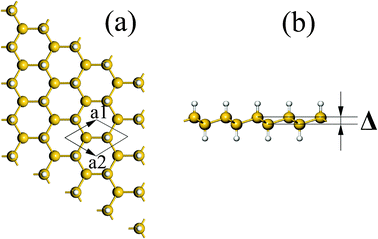 | ||
| Fig. 1 (a) Top and (b) side views of X-silicene in chair conformation. The primitive unit cell is delineated by dotted lines. Large and small balls denote Si and X atoms, respectively. | ||
3. Results and discussion
For the sake of comparison, H-silicene is considered firstly. An indirect Eg of 2.764 eV is obtained, which is larger than that of previous theoretic results within LDA.9 The valence band maximum (VBM) is located at the Γ point while the conduction band minimum (CBM) is at the M point, which are the same as given by other theoretical results.23,24We consider F-, Cl-, Br- and I-silicene, whose parameters are listed in Table 1. Δ = 0.694, 0.717, 0.705 and 0.677 Å, respectively, so all are more buckled than silicene (Δ = 0.44 Å).7 The bond angles between Si atoms of the four structures are 112°, 111°, 112° and 113°, respectively, indicating that Si atoms in X-silicenes exhibit sp3 hybridization and X-silicenes have near tetrahedral configurations. It is known that in silicene, the pz orbitals of adjacent Si atoms have reduced π–π overlap, and the structure thus has a mix of sp2 and sp3 hybridization. However in X-silicene, all Si atoms are saturated with sp3 hybridization. When halogens are adsorbed on silicene, the change in hybridization from a mix of sp2 and sp3 to sp3 results in more buckled structures. Such sp3 structures are responsible for the near tetrahedral configurations of X-silicenes. The Si–Si lengths (lSi–Si) in X-silicenes (2.398, 2.394, 2.406 and 2.449 Å, respectively) are larger than 2.281 Å in silicene (the literature value is 2.25 Å7). Meanwhile the lSi–X values in X-silicenes are 1.630, 2.085, 2.230 and 2.466 Å, respectively. The lSi–X values increase as the periodic number of the doping element (n) increases. The structural parameters for F-silicene are similar to recent theoretical results.25 Moreover, the structural variations of silicene upon halogen adsorption correspond to the case of the graphene–graphane transition.22 Note that with respect to lSi–Si = 2.371 Å for bulk Si, lSi–Si in silicene contracts to 2.281 Å due to the bonding nature (the former has a sp3 hybridization state while the latter is a mix of sp2 and sp3; the decrease of coordination number leads to the bond contraction and the lattice strain).
| Structure | a | l Si–Si | l Si–X | Δ | E f | E CBM | E VBM | E g |
|---|---|---|---|---|---|---|---|---|
| F-silicene | 3.977 | 2.398 | 1.630 | 0.694 | −1.982 | −3.775 | −5.244 | 1.469 |
| Cl-silicene | 3.956 | 2.394 | 2.085 | 0.717 | −1.018 | −2.591 | −4.570 | 1.979 |
| Br-silicene | 3.984 | 2.406 | 2.230 | 0.705 | −0.845 | −1.841 | −3.791 | 1.950 |
| I-silicene | 4.077 | 2.449 | 2.466 | 0.677 | −0.526 | −1.745 | −2.939 | 1.194 |
To evaluate the structural stability of X-silicenes, the formation energy Ef calculated is listed in Table 1, where Ef per atom is defined as,
| Ef = εSi–X − xSiεSi − xXεX | (1) |
All Ef values of X-silicene calculated based on eqn (1) are negative, indicating exothermic adsorptions and more stable structures with chemical bonding between halogen atoms and Si atoms. For H-silicene, Ef = −0.300 eV atom−1 in light of eqn (1), also being negative. Note that F molecules can react with Si on the bulk Si surface.26 Moreover, through the wet chemical process, treatment of H-terminated porous Si surface with molecular Cl, Br and I results in efficient Si–Cl, Si–Br and Si–I bond formation.27 The above reactions should also occur on silicene surface since the Si atoms in silicene are more reactive than those of bulk Si due to their mix of sp2 and sp3 hybridization nature. In fact, a similar case has been carried out in the synthesis of graphane.28
Due to the reactive and metastable nature of Si in silicene, in fact, silicene can only experimentally be synthesized on an Ag substrate in ultrahigh vacuum at present4 where the interaction between the substrate and the silicene increases the stability of silicene. Otherwise, Si atoms may easily assemble together and form a bulk Si structure. When silicenes are saturated by X atoms and form X-silicenes, X-silicenes are stabilized strongly with negative Ef values as shown in Table 1 where the sp3 bonding is similar to that of bulk Si. This is partly the reason why we consider X-silicenes as possible candidates for applications in FETs.
Due to the sp3 bonding of Si atoms, a gap of X-silicene is opened. As shown in Table 1, the Eg values of X-silicene are 1.469, 1.979, 1.950 and 1.194 eV, respectively, which are smaller than that of H-silicene (Eg = 2.764 eV). Moreover, both energy values of ECBM and EVBM of X-silicenes gradually increase as n increases.
The electronic structures are shown in Fig. 2. Both CBM and VBM are at the Γ point, denoting a direct band gap, which is consistent with the theoretical results for F-silicene.11,25 The difference of the minimum energy values in the conduction band (CB) between the value at the Γ point and that at the M point are 0.949, 0.307, 0.170 and 0.165 eV, respectively, gradually reducing with increasing n. Thus X reduces the minimum energy value of the CB at the Γ point more rapidly than that at the M point, which benefits the formation of a direct band gap.24 Consequently, halogens adsorbed on silicene not only reduce Eg, but also alter the gap to direct. For H-silicene, the Si–H bond is covalent. Those H electrons fill up the originally empty lowest CB of silicene. Thus, the bands are mostly intrinsic to silicene or Si–Si bonding.29 However, Si–X bonding contains ionic characteristics, where Mullican charge transfer values from Si to X are 0.64, 0.35, 0.22 and 0.11, respectively, with ηF, ηCl, ηBr and ηI values of 3.98, 3.16, 2.96, 2.66, respectively, which are much larger than ηSi = 1.90 (η denotes the Pauling electronegativity and the subscript denotes the corresponding element).30 The partly ionic characteristic of the Si–X bond diminishes the electron population in the bonding orbital of Si, weakens Si–Si bonding, and decreases the bonding–antibonding splitting and thus Eg. This bond weakening is confirmed by the Si–Si bond length elongation of lSi–Si = 2.394 Å in Cl-silicene and that of lSi–Si = 2.398 Å in F-silicene (the abnormal variation of lSi–Si for Br- and I-silicene will be discussed below). However, Eg values of X-silicene vary nonmonotonously where Eg (Br-silicene) > Eg (I-silicene), which should be clarified.
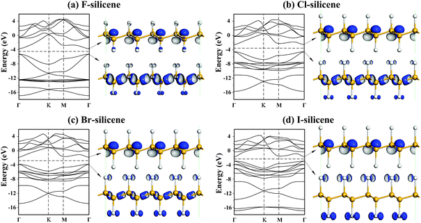 | ||
| Fig. 2 Electronic band structures (left) and charge density distributions of the CBM (right upper) and the VBM (right lower) states at the Γ point for (a) F-silicene, (b) Cl-silicene, (c) Br-silicene, and (d) I-silicene. The Fermi level is labeled with a dashed line. The isosurface value is 0.025 au. | ||
To understand this abnormal variation of Eg, charge density distributions are plotted in Fig. 2. The CBM of X-silicenes is mainly an antibonding state of Si-p orbitals, while the VBM is a mix of Si-p orbitals and X-p orbitals. As n increases, the VBM is contributed more by X-p orbitals, indicating the formation of surface states upon halogen functionalization. The interaction among these states is responsible for the dispersion of the CBM and VBM, and thus Eg.
The partial density of states (PDOS) of the four doped silicenes is shown in Fig. 3 where more details for Eg variation are given. The band edge characteristics induced by the halogens differ from those of H-silicene.29 Although the CBM is always determined by Si atoms, the VBM has distinct cases where Si–X bonding could have a direct effect on Eg. In Fig. 3(a) of F-silicene, most F states are located in the lower energy range of the valence band (VB). The energy level of the VBM thus mainly consists of Si-p orbitals and Si–X bonding has only an indirect effect. For Cl-silicene (Fig. 3(b)), a little weight of Cl states contribute to the VBM. The VBM of Br-silicene in Fig. 3(c) is almost equally determined by Si and Br atoms, while the VBM of I-silicene (Fig. 3(d)) is mainly decided by I-p orbitals and some I states even extend into the gap. Si–X bonding, especially for Br-silicene and I-silicene, contributes to Eg through the VBM, similar to the case of Si nanowires.10 In addition, the electron distribution of F states is more localized while that of I states is more dispersed, due to the gradually weakened ionic characteristics of Si–X bonding. As seen in Fig. 3(a)–(d), the VBs of X-silicenes gradually shift to higher energy zones, both Si-p orbitals and X-p orbitals, while X-p orbitals broaden more than Si-p orbitals. Br-silicene can be considered as the critical structure. The VBM of Br-silicene is determined almost equally by X-p and Si-p orbitals where the energy of the Si–Br bond ESi–Br is roughly equal to ESi–Si. Since ESi–I < ESi–Si, I-p orbitals determine the VBM. Moreover, the interaction between the halogen-p states and the surface Si atoms extends the Si-p band, and thus decreases ESi–Si with an increase in lSi–Si. This effect is more evident for Br- and I-silicenes, which leads to the abnormal variation of lSi–Si values in Br- and I-silicenes.
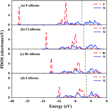 | ||
| Fig. 3 PDOS of F, Cl, Br and I (dashed line) and Si (solid line) for (a) F-silicene, (b) Cl-silicene, (c) Br-silicene, and (d) I-silicene. The Fermi level is labeled as a dashed line. | ||
According to energy band theory, the coupling of the interatomic potential and the respective Bloch wave functions, being proportional to the mean cohesive energy, determines the energy band identities as a common origin such as Eg. Halogens functionalization in silicene modulates ESi–Si and ESi–X, which induces a perturbation of the Hamiltonian, and thus Eg,31 while the increase (reduction) of bond energy increasing (decreasing) Eg.32 Clearly, in this work the competition between ESi–Si and ESi–X is responsible for the variation in Eg. As n increases, ESi–Si firstly increases for F- and Cl-silicenes, then decreases for Br- and I-silicenes where ESi–X decreases for all structures. For F-silicene, ESi–Si determines Eg and Eg has a smaller value (1.469 eV). For Cl-silicene, although ESi–Cl plays a more significant role, ESi–Si still dominates Eg where Eg increases (1.979 eV). Since ESi–Si is roughly equal to ESi–Br for Br-silicene, ESi–Br participates in the VBM. Their common effect leads to Eg of Br-silicene being almost equal to that of Cl-silicene (1.950 eV). I-silicene has a significant Egreduction (1.194 eV) since ESi–I determines VBM now.
To summarize the above results, Fig. 4 shows the Eg values of X-silicenes as a function of ηX − ηSi. H-silicene is taken as a reference. As n increases, ηX − ηSi gradually decreases. If both the band edges of X-silicenes are determined by ESi–Si, and ESi–X has little effect on ESi–Si, Eg should be a linear function of ηX − ηSi which in Fig. 4 is shown as a dashed line. The line is connected between the Eg of H-silicene and that of F-silicene. This is because the effect of ESi–H and ESi–F on Eg is less significant for H-silicene and F-silicene and can be ignored.29 However, the Eg values of Cl-, Br- and I-silicenes shown as solid balls deviate from the predicted Eg values which are shown as hollow balls on the straight dashed line. The deviations gradually become larger with increasing n which implies the effect of ESi–X.
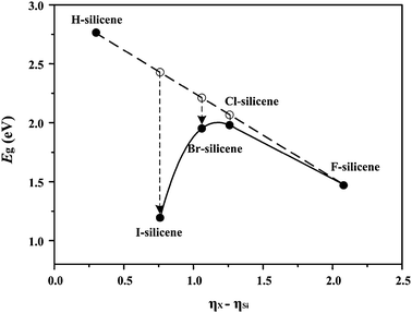 | ||
| Fig. 4 E g of X-silicenes as a function of ηX − ηSi. Solid and hollow balls denote true and predicted Eg values, respectively. | ||
Compared with the Eg values for X–Si nanowires with diameters of about 2 nm doped with F and Cl, the Eg values of F-silicene and Cl-silicene drop by 47% and 28%, being larger than that of Si nanowires by 11% and 7%, respectively.8 These evident differences result from the fact that the Eg of X-silicenes has no contribution from interior Si in nanowires while all Si atoms in X-silicenes are located on the surface. Thus, the effect of Egreduction induced by the ESi–Si drop is more evident for silicene than for nanowires. However, the reduction in Eg is almost the same for Br and I substitutions in X-Si nanowires and X-silicenes8 because ESi–X effects are almost the same for the two cases.
As shown above, the Eg values of F-silicene (1.469 eV) and I-silicene (1.194 eV) are closed to those of conventional channel materials of bulk GaAs (1.4 eV) and bulk Si (1.1 eV), respectively. Thus, F-silicene and I-silicene may be potential candidates for channel semiconductors of FETs and have compatibility with existing Si-based technology.
4. Conclusions
In summary, using DFT calculations with the sX-LDA function, we have calculated the electronic properties of silicene adsorbed with halogen elements. All of the structures have favorable formation energies, implying possible fabrication in the laboratory. Surface functionalization causes the Eg of silicene to open, and X-silicenes exhibit smaller Eg values than the hydrogenated structure. Moreover, the Eg values of X-silicenes firstly increase and then decrease, which is attributed to the competition of ESi–Si and ESi–X. As a result, the obtained F-silicene and I-silicene are possible candidates as channel materials for FETs.Acknowledgements
We acknowledge support from the National Key Basic Research, Development Program (Grant No. 2010CB631001) and the Program for Changjiang Scholars and Innovative Research Team in University, and High Performance Computing Center (HPCC) of Jilin University for supercomputer time.References
- F. Schwierz, Nat. Nanotechnol., 2010, 5, 487–496 CrossRef CAS.
- G. G. Guzman-Verri and L. C. L. Y. Voon, Phys. Rev. B: Condens. Matter Mater. Phys., 2007, 76, 075131–075140 CrossRef.
- H. Nakano, T. Mitsuoka, M. Harada, K. Horibuchi, H. Nozaki, N. Takahashi, T. Nonaka, Y. Seno and H. Nakamura, Angew. Chem., Int. Ed., 2006, 45, 6303–6306 CrossRef CAS.
- B. Lalmi, H. Oughaddou, H. Enriquez, A. Kara, S. Vizzini, B. Ealet and B. Aufray, Appl. Phys. Lett., 2010, 97, 223109–223110 Search PubMed.
- B. Aufray, A. Kara, S. Vizzini, H. Oughaddou, C. Leandri, B. Ealet and G. Le Lay, Appl. Phys. Lett., 2010, 96, 183102–183104 Search PubMed.
- K. Takeda and K. Shiraishi, Phys. Rev. B: Condens. Matter, 1994, 50, 14916–14922 CrossRef CAS.
- S. Cahangirov, M. Topsakal, E. Aktürk, H. Şahin and S. Ciraci, Phys. Rev. Lett., 2009, 102, 236804–236807 CrossRef CAS.
- R. Q. Zhang, X. M. Liu, Z. Wen and Q. Jiang, J. Phys. Chem. C, 2011, 115, 3425–3428 Search PubMed.
- L. C. L. Y. Voon, E. Sandberg, R. S. Aga and A. A. Farajian, Appl. Phys. Lett., 2010, 97, 163114–163116 CrossRef.
- P. W. Leu, B. Shan and K. J. Cho, Phys. Rev. B: Condens. Matter Mater. Phys., 2006, 73, 195320–195324 CrossRef.
- N. Lu, Z. Y. Li and J. L. Yang, J. Phys. Chem. C, 2009, 113, 16741–16746 Search PubMed.
- R. Asahi, W. Mannstadt and A. J. Freeman, Phys. Rev. B: Condens. Matter, 1999, 59, 7486–7492 Search PubMed.
- M. D. Segall, P. J. D. Lindan, M. J. Probert, C. J. Pickard, P. J. Hasnip, S. J. Clark and M. C. Payne, J. Phys.: Condens. Matter, 2002, 14, 2717–2744 CrossRef CAS.
- P. Hohenberg and W. Kohn, Phys. Rev., 1964, 136, B864–B871 CrossRef.
- W. Kohn and L. J. Sham, Phys. Rev., 1965, 140, A1133–A1138 CrossRef.
- D. M. Bylander and L. Kleinman, Phys. Rev. B: Condens. Matter, 1990, 41, 7868–7871 CrossRef.
- J. P. Perdew, K. Burke and M. Ernzerhof, Phys. Rev. Lett., 1996, 77, 3865–3868 CrossRef CAS.
- N. Troullier and J. L. Martins, Phys. Rev. B: Condens. Matter, 1991, 43, 1993–2006 CrossRef CAS.
- A. Seidl, A. Görling, P. Vogl, J. A. Majewski and M. Levy, Phys. Rev. B: Condens. Matter, 1996, 53, 3764–3774 CrossRef CAS.
- R. Gillen and J. Robertson, Phys. Rev. B: Condens. Matter Mater. Phys., 2010, 82, 125406–125410 Search PubMed.
- J. A. Yan, L. Yang and M. Y. Chou, Phys. Rev. B: Condens. Matter Mater. Phys., 2007, 76, 115319–115324 CrossRef.
- J. O. Sofo, A. S. Chaudhari and G. D. Barber, Phys. Rev. B: Condens. Matter Mater. Phys., 2007, 75, 153401–153404 CrossRef.
- S. D. Wang, L. Y. Zhu, Q. Chen, J. L. Wang and F. Ding, J. Appl. Phys., 2011, 109, 053516–053520 Search PubMed.
- C. G. Van de Walle and J. E. Northrup, Phys. Rev. Lett., 1993, 70, 1116–1119 Search PubMed.
- J. C. Garcia, D. B. de Lima, L. V. C. Assali and J. F. Justo, J. Phys. Chem. C, 2011, 115, 13242–13246 CrossRef CAS.
- D. P. Pullman, A. A. Tsekouras, Y. L. Li, J. J. Yang, M. R. Tate, D. B. Gosalvez, K. B. Laughlin, M. T. Schulberg and S. T. Ceyer, J. Phys. Chem. B, 2001, 105, 486–496 Search PubMed.
- J. M. Buriak, Chem. Rev., 2002, 102, 1271–1308 CrossRef CAS.
- D. C. Elias, R. R. Nair, T. M. G. Mohiuddin, S. V. Morozov, P. Blake, M. P. Halsall, A. C. Ferrari, D. W. Boukhvalov, M. I. Katsnelson, A. K. Geim and K. S. Novoselov, Science, 2009, 323, 610–613 CrossRef CAS.
- G. G. Guzman-Verri and L. C. L. Y. Voon, J. Phys.: Condens. Matter, 2011, 23, 145502–145506 CrossRef CAS.
- http://www.webelements.com/ .
- C. Q. Sun, Prog. Solid State Chem., 2007, 35, 1–159 CrossRef CAS.
- Y. F. Zhu, X. Y. Lang and Q. Jiang, Adv. Funct. Mater., 2008, 18, 1422–1429 Search PubMed.
| This journal is © the Owner Societies 2012 |