Substrate selected polymorphism of epitaxially aligned tetraphenyl-porphyrin thin films
Tatjana
Djuric
*a,
Thomas
Ules
b,
Sina
Gusenleitner
b,
Navaphun
Kayunkid
c,
Harald
Plank
d,
Gregor
Hlawacek
ef,
Christian
Teichert
e,
Martin
Brinkmann
c,
Mike
Ramsey
b and
Roland
Resel
a
aInstitute of Solid State Physics, Graz University of Technology, Austria. E-mail: tatjana.djuric@tugraz.at
bInstitute of Physics, Karl-Franzens University Graz, Austria
cInstitut Charles Sadron, CNRS - Université de Strasbourg, 23 rue du loess, 67034 Strasbourg, France
dInstitute for Electron Microscopy, Graz University of Technology, Austria
eInstitute of Physics, Montanuniversität Leoben, Austria
fPhysics of Interfaces and Nanomaterials, MESA + Institute for Nanotechnology, University of Twente, P.O. Box 217, 7500AE Enschede, The Netherlands
First published on 14th November 2011
Abstract
Porphyrin molecules, of interest as versatile materials for organic electronics, are highly prone to formation of significantly different polymorphic phases. To elucidate the determinants for the specific polymorphic phase formed in thin films as well as for the arrangement of the molecules on a given substrate two different anisotropic substrate surfaces have been selected: KCl(100) and the oxygen reconstructed Cu(110) surface. We observe that the crystal structure of the thin films depends on the substrate, whereas the relative molecular orientations in both cases are similar. X-Ray and transmission electron diffraction of 30 nm thick tetraphenyl-porphyrin (H2TPP) and platinum tetraphenyl-porphyrin (PtTPP) thin films deposited on KCl(100) surfaces reveals that both kinds of molecules crystallize in a tetragonal polymorph with the (001) lattice planes, i.e. with their macrocycles, parallel to the substrate. Films deposited on the oxygen reconstructed Cu(110)-(2 × 1)O surface exhibit in contrast the triclinic polymorph even though molecules again align nearly parallel to the substrate surface as observed by LEED and X-ray diffraction. On both substrates we identify two driving forces for the epitaxial alignment of porphyrins: (i) molecules aligning with their macrocycles (nearly) parallel to the substrate surface and (ii) the porphyrin molecules forming a commensurate unit cell with the respective substrate. The polymorphic phase meeting both requirements is the most favorable to be formed on a given substrate and due to this structural flexibility in both cases well-ordered, epitaxially aligned porphyrin thin films are achieved.
1. Introduction
Predicting and controlling the crystal structure as well as the molecular alignment of organic thin films are of crucial importance for the performance of organic thin film devices.1 Although often observed for crystals of organic molecules the phenomenon of polymorphism is still barely understood. Due to their weak and non-directional van der-Waals interactions, structures with significantly different molecular packings and thus different electronic properties can have similar lattice energies, i.e. in the thermodynamical sense have a similar likelihood of occurrence.2–4In this study we focus on characterizing thin films of porphyrin molecules, a group of organic compounds often used in organic opto-electronics and showing a pronounced tendency to polymorphism.5–9 Here, the crystal packing, molecular arrangement and morphological properties of epitaxially aligned thin films of tetraphenyl-porphyrin C44H30N4 (H2TPP) and its Pt-analogue C44H28N4Pt (PtTPP) are studied. H2TPP molecules consist of four phenyl groups which are attached to a highly conjugated porphine skeleton (macrocycle); two out of four nitrogen atoms located in the center of the macrocycle are bound to hydrogen atoms (Fig. 1a). The two hydrogen atoms are substituted by a platinum atom in the case of the metal complex PtTPP (Fig. 1b). Two competing forces are determining the final molecular configuration of porphyrins in crystals. On the one hand a planar macrocycle is advantageous. It ensures the most effective π–π-orbital overlapping as the molecules preferentially stack parallel to each other. On the other hand the molecules are driven for being packed as close as possible. Since the porphyrin molecules are easily deformed, several crystal structures are reported where the close packing is realized inducing a loss of the macrocycle planarity. In these crystal structures, the so called “ruffled” or “saddled” conformation is observed giving rise to the phenomenon of conformational polymorphism (i.e. chemically identical molecules adopt varying conformations in different crystal lattices).5–7 Though the bending and twisting of phenyl side groups in respect to the porphine skeleton is usually such that they are nearly perpendicular to the porphine skeleton, for specific polymorphic phases it also might significantly differ.
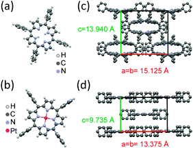 | ||
| Fig. 1 (a) Molecular structure of H2TPP (C44H30N4) and (b) its Pt-analogue PtTPP (C44H28N4Pt). Unit cells of the tetragonal polymorph I (c) and tetragonal polymorph II (d), respectively. | ||
Due to the highly conjugated macrocycles and the tendency to crystallize with the macrocycles parallel to each other, porphyrins have been recognized as promising materials for organic electronic devices, such as light-emitting diodes,10,11 photovoltaic cells12,13 or thin film transistors.14,15 Additionally, the easy substitution of the two central hydrogen atoms by a metal atom allows tuning the specific electronic and optical properties.16–18 Studies on thin films further show that those molecules form highly ordered arrays on various substrate surfaces. This is due to the high conformational flexibility of porphyrin molecules, which enables to adopt a conformation favorable for a specific substrate surface.19,20
Numerous recent studies have focused on the growth of porphyrins in ultra thin films solely using surface sensitive investigation techniques like LEED (low energy electron diffraction) and STM (scanning tunneling microscopy). Such studies barely go beyond the first monolayer and have not investigated crystallographic properties of porphyrin multilayer films.16,19,21–24 In the present study we go further: besides determining the impact of the substrate on the molecular arrangement we will explore which polymorphic phase most likely forms on a specific substrate. Two different well-defined, anisotropic substrates were selected for this purpose. The KCl(100) surface exhibiting a square 2d unit cell is a favored model surface reliably yielding epitaxially aligned films of organic molecules.25,26 The second substrate, oxygen reconstructed copper (110) (Cu(110)-(2 × 1)O), provides a corrugated surface due to orientation of adsorbed oxygen atom rows along the Cu[001] direction. For rodlike molecules it has been shown that the surface corrugation aligns the molecules and induces epitaxial order of the deposited molecules27 and in the present work this will be demonstrated also for the plate-like porphyrin molecules. The crystallographic and morphological properties of the porphyrin thin films are determined using LEED, X-ray diffraction techniques (XRD), transmission electron microscopy/diffraction (TEM/TED) as well as atomic force microscopy (AFM).
2. Experimental
Sample preparation
The oxygen reconstructed Cu(110) substrate surface was prepared by cleaning the copper crystal by repeated cycles of Ar+-ion bombardment and annealing it to 800 K. Dosing 10 L [1 Langmuir (L) = 1 Torr μs] of oxygen on the clean Cu(110) crystal at 500 K forms a p(2 × 1) added-row reconstruction which chemically polishes the surface.28 The resulting terraces are up to hundreds of nanometres wide and separated by monoatomic steps. In addition, oxygen exposure not only flattens out the substrate but also passivates it with respect to aromatic adsorption. The KCl(100) substrates were produced by cleaving a KCl single crystal under UHV with a homemade cleaver along the (100) plane. The H2TPP as well as PtTPP was deposited in situ from a thoroughly degassed evaporator with a pressure of 10−10 mbar. Nominal growth rates of 1–5 Å min−1, as monitored by a quartz microbalance, assuming a density of 1.273 and 1.688 g cm−3, respectively, were used.Low energy electron diffraction measurements
Low energy electron diffraction (LEED) experiments were performed in situ under ultra high vacuum on an Omicron MCP-LEED. Here, a micro channel plate is used to amplify electrons being backscattered by the sample. Due to this amplification only a low emission current in nA range is needed. The low primary beam current of the MCP-LEED allows sensitive samples, such as the studied porphyrin thin films, to be investigated without causing damage induced by higher beam current. In order to preserve the momentum of electrons parallel to the sample k∥, in the LEED pattern display a fringe field correction plate is used. However, close to the edge of the LEED screen little distortion is seen. With this setup a transfer width greater than 25 nm at 100 eV beam energy is reached.X-Ray diffraction measurements
The in situ prepared and characterized porphyrin multilayer films were removed from an UHV chamber for subsequent X-ray diffraction (XRD) measurements. Using a Philips X'pert X-ray diffractometer with CrKα radiation specular scans and pole figure measurements were performed. The measurement geometry of specular scans ensures that the scattering vector is always parallel to the surface normal of the substrate. By continuously varying its magnitude, lattice periodicities perpendicular to the substrate surface are probed determining the lattice planes of the thin film oriented parallel to the substrate surface. In contrast, pole figures are measured by keeping the magnitude of the scattering vector constant (e.g. choosing a specific lattice plane distance to be measured) while systematically changing its direction. Thereby, the distribution of lattice plane orientations of the substrate as well as of the organic thin film is obtained. From these measurements the azimuthal orientation of the thin film crystallites in respect to the substrate surface can be deduced. The simulation of pole figures was performed using STEREOPOLE29 and for the assignment of the peak positions measured in the specular scans POWDER CELL30 was used.The diffraction patterns of the H2TPP and PtTPP powders were measured with a Siemens D501 diffractometer in the focusing Bragg–Brentano geometry using CuKα radiation with a secondary graphite monochromator. The powder diffraction patterns were refined using the software MAUD.31
Transmission electron microscopy measurements
TEM was used as a complementary technique to determine the spatially resolved structure of the porphyrin films grown on KCl. The carbon coated H2TPP and PtTPP films were removed from the KCl substrate by floating onto water and were subsequently recovered onto TEM copper grids. TEM investigations were performed in bright field (BF) and selected area electron diffraction (SAED) modes using a Philips CM electron microscope (120 keV) equipped with a MVIII CCD camera. Calculation of the electron diffraction (ED) patterns was performed using WebEMAPS.32Atomic force microscopy measurements
Atomic Force Microscopy (AFM) measurements were performed ex situ using a Digital Instruments MultiMode AFM operated with a Nanoscope IIIa controller and a Digital Instruments Dimension 3100 AFM operated with a Nanoscope IVa controller. Regular silicon cantilevers with a typical resonance frequency of 300 kHz were used in tapping mode. The use of tapping mode ensures minimal lateral forces between the tip and the sample to preserve the original surface morphology of these sensitive films. Gwyddion33 and NanoScope [Version 1.2 by VEECO, 2010] software packages have been used for image analysis.3. Results and discussion
Powder diffraction
To specify to which extent the crystal structures formed in thin films depend on the nature of the substrate, the crystal structure of the ‘as-delivered’ porphyrin powders used for the preparation of the thin films was investigated by X-ray diffraction. The diffraction pattern obtained for the H2TPP powder (Fig. 2a) is in a good agreement with the simulated pattern of a body centered tetragonal structure reported by Hamor et al. (a = b = 15.125 Å, c = 13.940 Å; see Fig. 1c),34 though the unit cell parameters are slightly shifted to larger values: a = b = 15.2215 Å, c = 13.97 Å. Within small variations in the unit cell parameters identical crystal structure is also reported for many metal-substituted porphyrins such as CuTPP,6PdTPP, NiTPP6 as well as for PtTPP.7 The macrocycle lying in the (a,b) plane is ruffled and the porphyrin molecules are stacking along the c-direction. This structure exhibits the I![[4 with combining macron]](https://www.rsc.org/images/entities/char_0034_0304.gif) 2d space group, while the molecular symmetry is assigned to the D2d (2m) point group,35 accordingly describing the ruffled structure of the macrocycle. The two opposed phenyl rings do not lie in the same plane. They are twisted by an angle of 23° in respect to each other and enclose angles of 78.5° with the mean plane of the macrocycle.
2d space group, while the molecular symmetry is assigned to the D2d (2m) point group,35 accordingly describing the ruffled structure of the macrocycle. The two opposed phenyl rings do not lie in the same plane. They are twisted by an angle of 23° in respect to each other and enclose angles of 78.5° with the mean plane of the macrocycle.
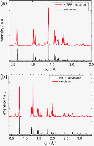 | ||
| Fig. 2 (a) Diffraction pattern of the H2TPP powder can be assigned to the tetragonal unit cell with the lattice parameters: a = b = 15.125 Å, c = 13.940 Å (tetragonal polymorph I). (b) The diffraction pattern for the PtTPP powder reveals a different tetragonal unit cell described by the following unit cell parameters: a = b = 13.3747 Å, c = 9.7348 Å (tetragonal polymorph II). The black lines in both cases show the simulated peak positions and intensities based on the assigned crystal structures. | ||
Though, only this crystal phase is explicitly reported for PtTPP,7 the diffraction pattern observed for the PtTPP powder (Fig. 2b) reveals a different body centered tetragonal unit cell, which is isomorphic (i.e. unit cell parameters are closely similar) with the structure previously reported for CuTPP:8a = b = 13.3747 Å, c = 9.7348 Å (Fig. 1d). Taking the reported CuTPP structure as a starting-point, the copper atoms were replaced by platinum atoms and the lattice parameters were slightly refined with a least-squares approach using the software MAUD (a = b = 13.345 Å, c = 9.719 Å). The lattice spacings calculated by using this adapted structure (black line) are in perfect accordance with the measured diffraction pattern (red line). There is a slight discrepancy in the intensity ratio probably induced by a preferential orientation of the crystallites due to the preparation of the powder for the measurement. Like in the tetragonal structure observed for H2TPP, the porphyrin molecules are stacked along the c-axis, but here the macrocycles are perfectly flat lying in the (a,b)-plane with phenyl groups perpendicular to it. The planar skeleton is described by the C4h (4/m) symmetry and this structure belongs to the I4/m space group.
It is worth emphasizing that in the observed crystal structures the Pt-analogue PtTPP adopts a planar structure in contrast to the metal-free H2TPP molecules. This peculiarity of porphyrin systems was already observed in the 1960s5,6 and points out that it is not the substitution with a metal atom which induces a conformational change leading to ruffled or saddle-like geometries but rather the specific forces of a given crystal structure. As the porphyrin molecules are easily deformable, crystal packing forces affect the final conformation of the molecules and therefore conformational polymorphism in porphyrin crystals is often observed.
For the purpose of this article the tetragonal phase observed for the H2TPP powder will be defined as ‘tetragonal polymorph I’, the phase observed for the PtTPP powder as ‘tetragonal polymorph II’.
Structure and alignment of tetraphenyl-porphyrins on KCl(100)
![(a) Bright field image of a PtTPP thin film (30 nm) grown on the KCl(100) substrate at room temperature. (b) Typical electron diffraction pattern of the PtTPP film reveals two single crystal diffraction patterns rotated by 36° in respect to each other. Panel (c) shows the calculated single crystal diffraction pattern assuming the [001] zone axis of the tetragonal polymorph II. (d) The bright field image of a H2TPP thin film (30 nm) grown on KCl(100) substrate at room temperature. (e) The diffraction pattern of the H2TPP thin film is basically the same as in the case of PtTPP, but here additional reflexes are visible (denoted by dashed circles). (f) Thus, it can be also explained by the tetragonal polymorph II assuming the same zone axis [001] but taking also the systematical forbidden reflexesh + k ≠ 2n into account.](/image/article/2012/CP/c1cp22299f/c1cp22299f-f3.gif) | ||
| Fig. 3 (a) Bright field image of a PtTPP thin film (30 nm) grown on the KCl(100) substrate at room temperature. (b) Typical electron diffraction pattern of the PtTPP film reveals two single crystal diffraction patterns rotated by 36° in respect to each other. Panel (c) shows the calculated single crystal diffraction pattern assuming the [001] zone axis of the tetragonal polymorph II. (d) The bright field image of a H2TPP thin film (30 nm) grown on KCl(100) substrate at room temperature. (e) The diffraction pattern of the H2TPP thin film is basically the same as in the case of PtTPP, but here additional reflexes are visible (denoted by dashed circles). (f) Thus, it can be also explained by the tetragonal polymorph II assuming the same zone axis [001] but taking also the systematical forbidden reflexesh + k ≠ 2n into account. | ||
The electron diffraction (ED) pattern of PtTPP grown on KCl(100) shows remarkably sharp diffraction spots indicative of a strong epitaxial alignment by the KCl substrate (Fig. 3b). A closer analysis reveals a superposition of two identical single crystal patterns which are rotated by 36° in respect to each other. The measured lattice spacings dhkl can be assigned to the tetragonal polymorph II which was observed for the PtTPP powder (a = 13.345 Å, c = 9.719 Å, space group: I4/m).8 The measured single crystal pattern is consistent with the calculated one of this structure assuming the [001] zone axis (Fig. 3c). This zone axis corresponds to the (001) contact plane and implies that molecules orient with their flat macrocycles parallel to the substrate surface.
Fig. 3e shows the electron diffraction pattern observed for H2TPP on KCl(100). Also here, we have two sets of identical single crystal patterns rotated by 36° in respect to each other. The measured lattice spacings e.g. d110 = 0.94 nm and d020 = 0.67 Å are the same as for the tetragonal polymorph II measured in the PtTPP film but interestingly the extinction rules imposed by the space group 87 are not fulfilled. Here, the reflection condition for the space group 87 (I4/m) (for (hk0): h + k = 2n, n: integer) is not obeyed and we are additionally measuring h + k ≠ 2nreflexes (see Fig. 3f). However, the conditions (00l): l = 2n and (0k0): k = 2n are still fulfilled and possible space groups are identified to be 94 (P42212) and 114 (P21c). The difference in the space group has implications for the symmetry of the molecules. While the molecular symmetry of the structure measured for the PtTPP (space group 87) is described by a D4h point group and implies a planar geometry of the porphyrin macrocycle, both space groups coming in question for the H2TPP crystals have different point groups (D4 and D2d respectively). These point groups have a reduced symmetry and may indicate ruffling of the molecules. Molecular ruffling described by the D2d point group was also observed for the H2TPP powder, where the molecules have crystallized in the tetragonal polymorph I5 (Fig. 1c and 2a).
In the crystallographic phases mentioned above the H2TPP molecules obviously exhibit a four-fold inversion symmetry axis5 (this is also valid for porphines in general39). At first sight this might be surprising, as only two out of four nitrogen atoms located diagonally opposite in the center of the porphine ring are bound to hydrogen atoms. These pyrrole rings are distinguishable from the other two and therefore the porphine core is determined by a two-fold rotational axis. The fact, that nevertheless a 4-fold molecular symmetry is experimentally observed, has been explained by a statistical distribution of the inner hydrogen atoms.5,39,40
The molecular orientation deduced from ED patterns is further corroborated by the HR-TEM image of the PtTPP thin film, which corresponds to a two dimensional projection of the crystallites (Fig. 4). The contrast in the HR-TEM image showing a periodic modulation (Fig. 4a) arises from the Z-contrast between the Pt cores and the organic macrocycle. The Fast Fourier Transform (FFT) in the inset shows two pairs of perpendicular directions (indicated by red and blue circles, respectively) along which a periodicity of 9.0 ± 0.5 Å is observed. Hence, the analysis of the HR-TEM image and the corresponding Fast Fourier Transform (FFT) in the inset yields two square lattices which are rotated by 36.7° in respect to each other. In the HR-TEM image these two differently oriented domains containing squared periodicities are labeled (I) and (II) and marked with blue and red dashed lines, respectively. The occurrence of two square lattices with a 9.0 ± 0.5 Å period and two different in-plane orientations at a relative angle of 36.7° is in accordance with the angle of 36° observed in the ED pattern of PtTPP (Fig. 3b). The period of the lattice observed by HR-TEM is in good accordance with the calculated lattice spacing of d110 = 9.46 Å for the tetragonal polymorph II. As PtTPP crystallizes in a body centered structure, the projection along the c axis, corresponding to a (001) contact plane as observed in ED pattern, yields an apparent square lattice with a period equal to d110. The insets in Fig. 4(b) and (c) depict the corresponding molecular packing of the Pt-TPP molecules in the tetragonal polymorph II along the c-axis projection. The dashed lines correspond to the (110) and (![[1 with combining macron]](https://www.rsc.org/images/entities/char_0031_0304.gif) 10) lattice planes, defining a grating with a periodicity of d110 = 9.46 Å as observed in the HR-TEM image. This result supports the body-centered structure of the Pt-TPP in epitaxied layers on KCli.e. a structure isomorphous to the polymorph II evidenced in powders. This implies that epitaxy of Pt-TPP on KCl does not induce a specific thin film phase.
10) lattice planes, defining a grating with a periodicity of d110 = 9.46 Å as observed in the HR-TEM image. This result supports the body-centered structure of the Pt-TPP in epitaxied layers on KCli.e. a structure isomorphous to the polymorph II evidenced in powders. This implies that epitaxy of Pt-TPP on KCl does not induce a specific thin film phase.
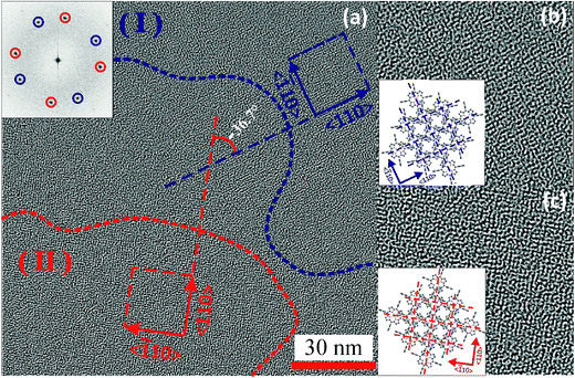 | ||
| Fig. 4 (a) The high-resolution TEM image of PtTPP grown on KCl(100) substrate. The corresponding FFT image is shown in the inset. The blue and red colors indicate the different oriented domains: (I) and (II). The dotted lines represent the boundaries of oriented crystalline domains and the arrows indicate the crystallographic directions in the domains. The figure (b) and (c) are the enlarged HR-TEM images (38 nm × 38 nm) of the domains (I) and (II), respectively. The enlarged figures apparently display similar net-like morphology in both domains but in different orientations. The angle between 2 orientations is ∼36.7° as shown in (a) similar to XRD. The insets of (b) and (c) are models showing the molecular orientation of PtTPP networks in each domain. | ||
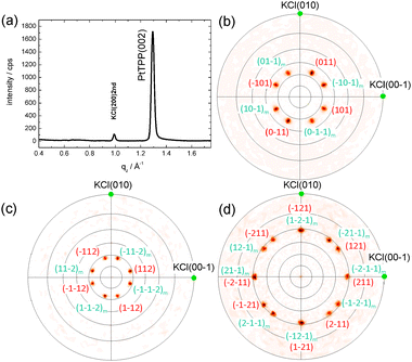 | ||
| Fig. 5 (a) Specular scan of a 30 nm thick PtTPP film grown on KCl(100). Pole figures measured for net planes (b) (101) with d = 0.787 nm, (c) (112) with d = 0.433 nm and (d) (211) with d = 0.510 nm reveal two epitaxially well-aligned domains, which are mirrored in respect to the substrate azimuths (denoted with indices in red and blue). The relative azimuthal orientation of the KCl(100) substrate is denoted by green circles. | ||
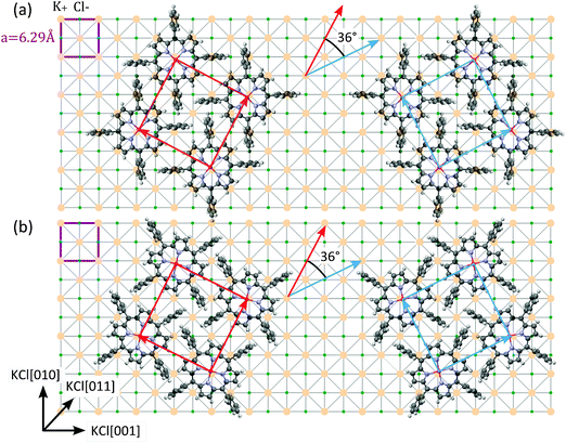 | ||
| Fig. 6 Epitaxial alignment of PtTPP domains on the KCl(100) surface substrate in top-view. PtTPP crystallites are oriented with the (001) net plane parallel to the substrate surface and form a commensurate square unit cell with a = 13.375 Å. Lattices of the two molecular arrangements shown in (a) and (b) are indistinguishable as they yield the same diffraction pattern in the pole figures. | ||
Molecules lying in the (001) contact plane form a square unit cell with the cell parameter a = 1.345 nm. The dimensions of this unit cell are in accordance with the usually reported monolayer structure for systems of porphyrin molecules16,18,41,42 suggesting that the alignment of the monolayer molecules basically is preserved when films in multilayer range are grown. When a lattice mismatch of 5% is taken into account, the epitaxial relationship with the underlying KCl(100) substrate can be described by the following commensurable epitaxial matrix

An AFM image recorded on the 30 nm thick PtTPP film grown on KCl(100) is shown in Fig. 7. The morphology shows preferred alignment of the features, which is reflected in the Fourier transform in the inset. The relative azimuthal alignment of the crystallites (dashed white lines) in respect to the substrate (horizontal/vertical lines) enclosing an angle of (33 ± 4)° is in good accordance with the alignment of the 2D unit cells deduced from XRD measurements.
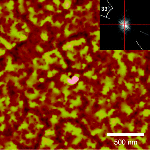 | ||
| Fig. 7 AFM image of a 30 nm PtTPP film grown on KCl(100). The inset shows the Fourier transform of the image. The dashed white lines denote the preferential alignment of the PtTPP crystallites in respect to the substrate azimuths (solid red lines). | ||
Structure and alignment of tetraphenyl-porphyrins on Cu(110)-(2 × 1)O
 | (1) |
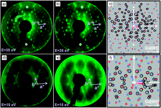 | ||
| Fig. 8 LEED images of H2TPP and PtTPP monolayers grown on Cu(110)-(2 × 1)O are shown in (a) and (b), respectively, and reveal the same diffraction pattern. (c) The measured diffraction patterns (black circles) can be explained by two mirrored domains (red and blue spots) forming a unit cell with dimensions: a = (1.53 ± 0.05) nm, b = (2.57 ± 0.05) nm and γ = 78.57°. The corresponding LEED measurements of the 3 nm multilayer films are shown in (d) for H2TPP and (e) for PtTPP. The pattern shown in (f) is calculated using basically the same unit cell as observed for the monolayer. | ||
 lattice plane being parallel to the substrate. The structure factor for this lattice plane equals zero, explaining the absence of diffraction intensity stemming from the thin film in the specular scan. The side view of the molecules oriented with the
  lattice plane parallel to the surface (Fig. 10b) illustrates that also in this system H2TPP molecules have adopted an orientation where the porphyrin rings are nearly parallel to the substrate with a tilt of only 9° in respect to it. Fig. 10c shows the arrangement of the molecules on the oxygen reconstructed Cu substrate in top view. The [
![[7 with combining macron]](https://www.rsc.org/images/entities/char_0037_0304.gif)
![[3 with combining macron]](https://www.rsc.org/images/entities/char_0033_0304.gif) 2] direction of the H2TPP crystallites is determined to be parallel to the [001] direction of the oxygen reconstructed copper surface; this means that H2TPP molecules align epitaxially with diametrically opposite phenyl rings along the oxygen rows of the CuO surface reconstruction (see Fig. 10c). The commensurate unit cell deduced from the monolayer LEED measurements and described by the epitaxial matrix M2 is very close to the 2D unit cell deduced from the molecules lying in the
2] direction of the H2TPP crystallites is determined to be parallel to the [001] direction of the oxygen reconstructed copper surface; this means that H2TPP molecules align epitaxially with diametrically opposite phenyl rings along the oxygen rows of the CuO surface reconstruction (see Fig. 10c). The commensurate unit cell deduced from the monolayer LEED measurements and described by the epitaxial matrix M2 is very close to the 2D unit cell deduced from the molecules lying in the  net plane with only a 5% mismatch. Further, in Fig. 10c it is seen that the packing of the molecules is not as dilute as expected from the unit cell dimensions deduced from the LEED measurements. At a distance of only 0.2 nm there is a second plane B containing porphyrin molecules which have the same molecular orientation with respect to the substrate. The molecules in this plane form an identical commensurate unit cell but with an origin shifted by a vector of s = (3,2) (i.e.3aCu, 2bCu) with respect to the unit cell lying in plane A. Taking this second plane into account, the coverage of the porphyrin molecules is rather dense. In the side-view (see Fig. 10b) the position of these two planes is indicated.
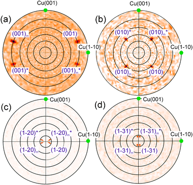 | ||
Fig. 9
Pole figures of the H2TPP multilayer film grown on the Cu(110)-p(2 × 1) substrate are measured at different dhkl values: (a) d001 = 12.13 Å, (b) d010 = 10.12 Å, (c) d1![[2 with combining macron]](https://www.rsc.org/images/entities/char_0032_0304.gif) 0 = 4.41 Å, (d) d11 = 3.19 Å. Pole figures reveal that crystallites arrange in epitaxially oriented domains with the 0 = 4.41 Å, (d) d11 = 3.19 Å. Pole figures reveal that crystallites arrange in epitaxially oriented domains with the  net plane parallel to the substrate surface. The relative azimuthal orientation of the KCl(100) substrate is denoted by green circles. net plane parallel to the substrate surface. The relative azimuthal orientation of the KCl(100) substrate is denoted by green circles. | ||
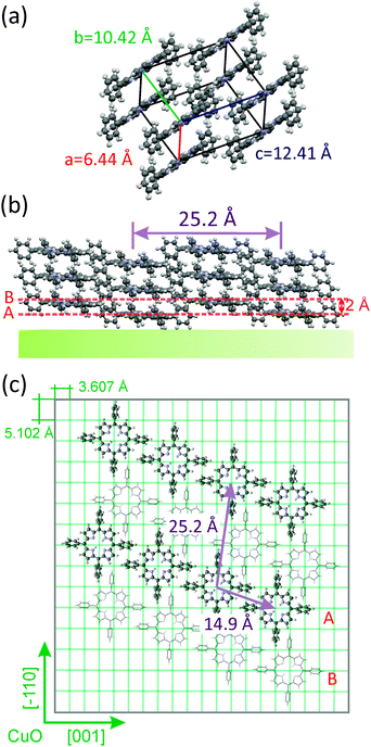 | ||
Fig. 10 (a) Unit cell of the triclinic polymorph observed in a 37 nm thick H2TPP film grown on a Cu(110)-(2 × 1)O surface. (b) Side view of H2TPP molecules orienting with the  net plane parallel to the Cu(110)-(2 × 1)O substrate. (c) Alignment of H2TPP molecules on the oxygen reconstructed Cu(110) surface in top view. net plane parallel to the Cu(110)-(2 × 1)O substrate. (c) Alignment of H2TPP molecules on the oxygen reconstructed Cu(110) surface in top view. | ||
The surface morphology of the same H2TPP multilayer film (37 nm) was characterized using AFM. The 5 × 5 μm2AFM image shown in Fig. 11a reveals a rather uniform, granular morphology which is reminiscent of that observed for porphyrins on the KCl(100) surface (compare Fig. 3a and d). The crystallites have an average aspect ratio of 1![[thin space (1/6-em)]](https://www.rsc.org/images/entities/char_2009.gif) ∶1.4 and a projected area of 0.013 μm2 (130 nm × 90 nm). On a smaller scale (inset in Fig. 11a) it becomes evident that crystallites line up forming linear structures with a correlation length of up to 500 nm. Fig. 11b shows a 1 × 1 μm2 detail of the surface. The crystals exhibit a limited number of well oriented facets. Since the AFM topography image represents the three-dimensional morphology z(x,y), it can be analyzed in terms of the orientation of the local surface normals finally yielding integral information on the facet orientations.45,46 The corresponding slope distribution, obtained by fitting a local plane through the neighborhood of each point and using its gradient, is given in the inset of Fig. 11b. The distance of a point to the center corresponds to the inclination of the local plane while the polar position represents the in-plane orientation of the local surface normal. It shows that the most frequent facet's normals found have an inclination angle of 29° ± 5° (measured from the substrate surface normal) and are separated azimuthally 76° ± 8° (dashed lines). These inclination angles fit with the angles enclosed by the low-indexed planes like (10) (24.2°) and (11) (27.9°) with the
∶1.4 and a projected area of 0.013 μm2 (130 nm × 90 nm). On a smaller scale (inset in Fig. 11a) it becomes evident that crystallites line up forming linear structures with a correlation length of up to 500 nm. Fig. 11b shows a 1 × 1 μm2 detail of the surface. The crystals exhibit a limited number of well oriented facets. Since the AFM topography image represents the three-dimensional morphology z(x,y), it can be analyzed in terms of the orientation of the local surface normals finally yielding integral information on the facet orientations.45,46 The corresponding slope distribution, obtained by fitting a local plane through the neighborhood of each point and using its gradient, is given in the inset of Fig. 11b. The distance of a point to the center corresponds to the inclination of the local plane while the polar position represents the in-plane orientation of the local surface normal. It shows that the most frequent facet's normals found have an inclination angle of 29° ± 5° (measured from the substrate surface normal) and are separated azimuthally 76° ± 8° (dashed lines). These inclination angles fit with the angles enclosed by the low-indexed planes like (10) (24.2°) and (11) (27.9°) with the  lattice plane, which is parallel to the substrate surface. The azimuthal orientation of the crystallites corresponds well to the two mirrored domains which are rotated by 40° to each other as determined by XRD.
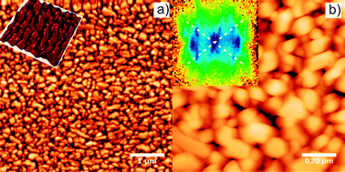 | ||
| Fig. 11
AFM images of a 37 nm thick H2TPP film grown on Cu(110)-(2 × 1)O. (a) Crystallites with a size of 0.013 μm² and an average aspect ratio of 1∶1.4 are observed (z-scale 50 nm). The inset is a 3D representation of 1 μm detail which clearly demonstrates that the crystals are aligned. (b) 1 μm detail of the H2TPP film showing facetted crystallites. The inset displays the slope distribution (x,y range from −1 to 1 or −45° to 45°) found in the image. Facets with an inclination angle of 29° ± 5° are most common (dashed lines). The two dominant azimuthal directions of the facet normals are separated by 76° ± 8°. | ||
4. Discussion
The crystal structures measured in porphyrin powders are used as a starting point to discuss the impact of the substrate surface on the polymorphic phase appearing in porphyrin thin films. In powder, H2TPP and PtTPP crystallize in two different tetragonal polymorphs. The tetragonal polymorph I (a = b = 15.2215 Å, c = 13.97 Å) with a ruffled macrocycle was found for the H2TPP powder, while in the PtTPP powder the tetragonal polymorph II (a = b = 13.345 Å, c = 9.719 Å) with a flat macrocycle was observed.We have found that in thin films, molecules of tetraphenyl-porphyrins adopt different polymorphic structures depending on the nature of the substrate surfaces (schematically summarized in Fig. 12). When deposited on KCl(100) substrates both porphyrin molecules (H2TPP and PtTPP) crystallize in the tetragonal polymorph II with their macrocycles oriented parallel to the substrate surface. The relative azimuthal orientation of the formed 2D unit cell is commensurable with the 2D unit cell of the KCl(100) substrate. The software Epicalc43 based on geometric lattice misfit modeling calculates exactly the same azimuthal orientation as the most favorable for this 2D unit cell. This underlines that the minimization of the lattice mismatch is a driving force for the observed epitaxial alignment in this system. By contrast, for molecules lying in the (001) lattice plane of the tetragonal polymorph I (corresponding to macrocycles oriented parallel to the substrate) no commensurable arrangement is possible, making this polymorphic phase less favorable to be formed on the KCl(100) substrate.
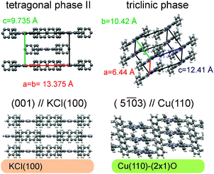 | ||
| Fig. 12 Schematic diagram summarizing the polymorphic phases and preferential orientations of tetraphenyl-porphyrin thin films deposited on KCl(100) and Cu(110)-(2 × 1)O substrates, respectively. The relative orientation of the molecules in respect to the selected substrate surface is depicted in the bottom row. The top row shows the polymorphic phases appearing on respective substrate surfaces. | ||
On the Cu(110)-(2 × 1)O surface the porphyrin macrocycles are oriented nearly parallel to the substrate surface and crystallize in a triclinic polymorphic phase, a polymorph not observed in the powders. Using the geometric lattice matching routine Epicalc the azimuthal orientation of the 2D unit cell forming a commensurable structure as observed by LEED and pole figure measurements is predicted to be the most favorable. If we take the 2D unit cell of the tetragonal polymorph II observed on the KCl(100) substrate into account and calculate the most favorable epitaxial alignment on the Cu(110)-(2 × 1)O surface, no commensurate structure is found. This gives a possible explanation why on the oxygen reconstructed Cu(110) surface the triclinic phase is more favorable than the tetragonal polymorph II.
The open question that remains is why on the Cu(110)-(2 × 1)O surface the porphyrin molecules do not crystallize in the tetragonal polymorphic phase I. The (001) net plane of this structure contains the macrocycles and for the square unit cell formed by the molecules lying in this plane (a = b = 1.5125 nm) azimuthal orientation yielding a commensurate unit cell would be possible. We suggest that it is the conformation of porphyrin molecules in the tetragonal phase I which makes this polymorph less favorable for the accommodation on the strongly corrugated Cu(110)-(2 × 1)O surface. In the triclinic structure the phenyl rings are not perpendicular to the macrocycle, as also was evidenced by NEXAFS studies of these films,47 but enclose an angle of approx. 62° with it. This finding is in accordance with studies reporting a bending of phenyl rings when porphyrins are deposited on metallic surfaces.19 However, in the triclinic structure the opposed phenyl rings lie in the same plane, whereas in the case of the tetragonal phase I their planes are twisted by an angle of approximately 23°. As the corrugation of the Cu(110)-(2 × 1)O surface induces an epitaxial alignment of molecules parallel to the oxygen rows (e.g. along the corrugation trenches) the triclinic phase with the untwisted opposed phenyls might be more favorable to arrange itself to the surface corrugation than the tetragonal phase. Taking this finding into account, we suggest that also in the case of porphyrin molecules deposited on the KCl(100) substrate, the phenyl rings will preferentially align along the principle symmetry axes of the substrate making the alignment depicted in Fig. 6(a) more reasonable than that in Fig. 6(b).
5. Conclusions
This work shows the high structural adaptability of porphyrin molecules leading to an extraordinarily pronounced polymorphism with the substrate determining not only the crystallite orientation but also the polymorph that grows on it. In particular, we have investigated the structural and morphological properties of well-ordered and epitaxially aligned porphyrin thin films deposited on two different substrates. On the Cu(110)-(2 × 1)O surface the porphyrins crystallize in a rather unusual triclinic phase for thin films with macrocycles nearly parallel to the substrate. In contrast, on the KCl(100) substrate we observe the tetragonal polymorph II exhibiting the (001) contact plane containing the flat lying macrocycles. In all cases, the porphyrin molecules form a commensurate unit cell with the respective substrate ensuring the most effective geometric lattice matching. Based on these results two main driving forces for the epitaxial growth of porphyrins on the observed anisotropic surfaces are identified: (i) alignment of macrocycles parallel to the substrate surface forming molecular columns in a subsequent step of crystallization and (ii) minimization of the lattice mismatch between the adsorbate and the substrate unit cell. These two requirements determine which polymorphic phase is most likely realized on a given substrate surface.Acknowledgements
This work was supported by the Austrian Science Fund (FWF): [P21094] and [S9708].References
- A. A. Virkar, S. Mannsfeld, Z. Bao and N. Stingelin, Adv. Mater., 2010, 22, 3857–3875 CrossRef CAS.
- C. Ambrosch-Draxl, D. Nabok, P. Puschnig and C. Meisenbichler, New J. Phys., 2009, 11, 125010 CrossRef.
- S. L. Price, Acc. Chem. Res., 2009, 42, 117–126 CrossRef CAS.
- J. Bernstein, J. Phys. D: Appl. Phys., 1993, 26, B66–B76 CrossRef CAS.
- M. J. Hamor, T. A. Hamor and J. L. Hoard, J. Am. Chem. Soc., 1964, 86, 1938–1942 CrossRef CAS.
- E. B. Fleischer, C. K. Miller and L. E. Webb, J. Am. Chem. Soc., 1964, 86, 2342–2347 CrossRef CAS.
- A. C. Hazell, Acta Crystallogr., Sect. C: Cryst. Struct. Commun., 1984, 40, 751–753 CrossRef.
- H.-S. He, Acta Crystallogr., Sect. E: Struct. Rep. Online, 2007, 63, m976–m977 Search PubMed.
- S. J. Silvers and A. Tulinsky, J. Am. Chem. Soc., 1967, 89, 3331–3337 CrossRef CAS.
- C.-M. Che, Y.-J. Hou, M. C. W. Chan, J. Guo, Y. Liu and Y. Wang, J. Mater. Chem., 2003, 13, 1362 RSC.
- R. C. Kwong, S. Sibley, T. Dubovoy, M. Baldo, S. R. Forrest and M. E. Thompson, Chem. Mater., 1999, 11, 3709–3713 CrossRef CAS.
- M. G. Walter, A. B. Rudine and C. C. Wamser, J. Porphyrins Phthalocyanines, 2010, 14, 759 CrossRef CAS.
- T. Bessho, S. M. Zakeeruddin, C.-Y. Yeh, E. W.-G. Diau and M. Grätzel, Angew. Chem., Int. Ed., 2010, 49, 6646–6649 CrossRef CAS.
- C. Che, H. Xiang, S. S. Chui, Z. Xu, V. A. L. Roy, J. J. Yan, W. Fu, P. T. Lai and I. D. Williams, Chem.–Asian J., 2008, 3, 1092–1103 CrossRef CAS.
- P. Checcoli, Synth. Met., 2003, 138, 261–266 CrossRef CAS.
- L. Scudiero, D. E. Barlow, U. Mazur and K. W. Hipps, J. Am. Chem. Soc., 2001, 123, 4073–4080 CrossRef CAS.
- F. Buchner, V. Schwald, K. Comanici, H.-P. Steinrück and H. Marbach, ChemPhysChem, 2007, 8, 241–243 CrossRef CAS.
- W. Auwärter, A. Weber-Bargioni, S. Brink, A. Riemann, A. Schiffrin, M. Ruben and J. V. Barth, ChemPhysChem, 2007, 8, 250–254 CrossRef.
- F. Moresco, G. Meyer, K.-H. Rieder, J. Ping, H. Tang and C. Joachim, Surf. Sci., 2002, 499, 94–102 CrossRef CAS.
- T. A. Jung, R. R. Schlittler and J. K. Gimzewski, Nature, 1997, 386, 696–698 CrossRef CAS.
- F. Buchner, I. Kellner, W. Hieringer, A. Görling, H.-P. Steinrück and H. Marbach, Phys. Chem. Chem. Phys., 2010, 12, 13082 RSC.
- P. Donovan, A. Robin, M. S. Dyer, M. Persson and R. Raval, Chem.–Eur. J., 2010, 16, 11641–11652 CrossRef CAS.
- D. E. Barlow, L. Scudiero and K. W. Hipps, Langmuir, 2004, 20, 4413–4421 CrossRef CAS.
- F. Buchner, K. Comanici, N. Jux, H.-P. Steinruck and H. Marbach, J. Phys. Chem. C, 2007, 111, 13531–13538 CAS.
- S.-i. Yanagiya, H. Wakamatsu, O. Nishikata and T. Inoue, Jpn. J. Appl. Phys., 2004, 43, 7722–7724 CrossRef CAS.
- T. Haber, M. Oehzelt, R. Resel, A. Andreev, A. Thierry, H. Sitter, D.-M. Smilgies, B. Schaffer, W. Grogger and R. Resel, J. Nanosci. Nanotechnol., 2006, 6, 698–703 CrossRef CAS.
- M. Koini, T. Haber, O. Werzer, S. Berkebile, G. Koller, M. Oehzelt, M. Ramsey and R. Resel, Thin Solid Films, 2008, 517, 483–487 CrossRef CAS.
- K. Kern, H. Niehus, A. Schatz, P. Zeppenfeld, J. Goerge and G. Comsa, Phys. Rev. Lett., 1991, 67, 855–858 CrossRef CAS.
- I. Salzmann and R. Resel, J. Appl. Crystallogr., 2004, 37, 1029–1033 CrossRef CAS.
- W. Kraus and G. Nolzeb, J. Appl. Crystallogr., 1996, 29, 301–303 CrossRef CAS.
- L. Lutterotti, M. Bortolotti, G. Ischia, I. Lonardelli and H.-R. Wenk, Z. Kristallogr., 2007, 2007, 125–130 CrossRef.
- J. M. Zuo and J. C. Mabon, Microsc. Microanal, 2004, 10(suppl. 2), 1000–1001 Search PubMed.
- P. Klapetek, D. Necas and C. Anderson, Gwyddion user guide, 2011 Search PubMed.
- M. J. Hamor, T. A. Hamor and J. L. Hoard, J. Am. Chem. Soc., 1964, 86, 1938–1942 CrossRef CAS.
- T. Hahn, H. Fuess, T. Hahn, H. Wondratschek, U. Müller, U. Shmueli, E. Prince, A. Authier, V. Kopský, D. B. Litvin, M. G. Rossmann, E. Arnold, S. Hall and B. McMahon, 1. Aufl., International Tables for Crystallography, International Union of Crystallography, Chester, England, 2006, Bd. A Search PubMed.
- S. Hayashi, H. Yanagi, Y. Ueda, Y. Fujiyoshi and M. Ashida, Ultramicroscopy, 1993, 49, 308–317 CrossRef CAS.
- M. Ashida, H. Yanagi, S. Hayashi and K. Takemoto, Acta Crystallogr., Sect. B: Struct. Sci., 1991, 47, 87–91 CrossRef.
- H. Yanagi and T. Shibutani, Thin Solid Films, 2003, 438–439, 33–38 CrossRef CAS.
- L. E. Webb and E. B. Fleischer, J. Chem. Phys., 1965, 43, 3100 CrossRef CAS.
- E. D. Becker, R. B. Bradley and C. J. Watson, J. Am. Chem. Soc., 1961, 83, 3743–3748 CrossRef CAS.
- F. Buchner, V. Schwald, K. Comanici, H.-P. Steinrück and H. Marbach, ChemPhysChem, 2007, 8, 241–243 CrossRef CAS.
- L. Scudiero, D. E. Barlow, U. Mazur and K. W. Hipps, J. Am. Chem. Soc., 2001, 123, 4073–4080 CrossRef CAS.
- J. A. Last, D. E. Hooks, A. C. Hillier and M. D. Ward, J. Phys. Chem. B, 1999, 103, 6723–6733 CrossRef CAS.
- L. G. Teugels, L. G. Avila-Bront and S. J. Sibener, J. Phys. Chem. C, 2011, 115, 2826–2834 CAS.
- M. Lutz, R. Feenstra, P. Mooney, J. Tersoff and J. Chu, Surf. Sci., 1994, 316, L1075–L1080 CrossRef CAS.
- C. Teichert, Phys. Rep., 2002, 365, 335–432 CrossRef CAS.
- S. Gusenleitner, Geometric and Electronic Structure of Tetraphenylporphyrin and Tetraphenylporphyrin Pt(II) on Cu(110) and Cu(110)p(2×1)O, University Graz, 2009 Search PubMed.
| This journal is © the Owner Societies 2012 |