All-carbon electrode-based fiber-shaped dye-sensitized solar cells†
Received
15th August 2011
, Accepted 1st September 2011
First published on 19th September 2011
Abstract
A novel fiber-shaped dye-sensitized solar cell (DSSC) based on an all-carbon electrode is presented, where low-cost, highly-stable, and biocompatible carbon materials are applied to both the photoanode and the counter electrode. The fibrous carbon-based photoanode has a core–shell structure, with carbon fiber core used as conductive substrate to collect carriers and sensitized porous TiO2 film as shell to harvest light effectively. The highly catalytic all-carbon counter electrode is made from ink carbon coatings and carbon fiber substrate. Results show that the open circuit voltage can be largely improved through engineering at the carbon fiber/TiO2 interface. An optimized diameter of the photoanode results in an efficiency of 1.9%. It is the first demonstration of efficient DSSCs based on all-carbon electrodes, and the devices are totally free from TCOs or any other expensive electrode materials. Also, this type of solar cell is significant in obtaining bio-friendly all-carbon photovoltaics suitable for large-scale production.
Introduction
Dye-sensitized solar cells (DSSCs) have received considerable attention from the academic community and industry for their outstanding advantages, namely, easy to produce, high efficiency and environmental-friendliness.1,2 Although the light-to-electricity conversion efficiency (η) of liquid DSSC has reached 11%–12%,3,4 quite a few challenges remain to be addressed before its commercialization, including cost, performance and long-term stability. Traditional planar DSSCs generally use expensive transparent conductive oxide (TCO, such as fluorine-doped tin oxide, FTO) glasses as electrode conductive substrates. TCO glass suffers from drawbacks like high sheet resistance, rigidity, and heavy weight, and thus it is not applicable for large-scale production,5 or in fabricating lightweight and flexible devices. Hence, the search for low-cost, highly stable, environmental and flexible conductive substrates or exploring new-type device structures have always been crucial issues in photovoltaic research. Among studies reported, metallic materials with high conductivity and resistance to high-temperature sintering are applied to highly efficient planar DSSCs as conductive photoanode substrates.6–9 However, constrained by the light-transmission mode of traditional planar cells, the other electrode of the device still needs expensive TCO materials. As an alternative to traditional planar photovoltaics, fiber-shaped photovoltaics with three-dimensional light harvesting ability have aroused great interest. Fiber-shaped solar cells exhibit higher flexibility in the choice of substrate materials,10–13 lighting pattern, and light-coupling utilization,14,15 which greatly facilitates the development of highly efficient, low-cost solar cell modules and woven electronics applied in specific fields.
The family of carbon materials comprises a wide range of excellent materials, from industrial grade graphite, activated carbon, and carbon black to carbon nanotubes, fullerene, and graphene used in fundamental research. Along with the aggravation of energy and environmental issues, these cost-effective carbon materials are also extensively applied to fuel cells,16lithium batteries,17 and photovoltaics.18 Intense research has focused on using highly stable carbon materials with large specific area and high catalytic activity as catalysts for the counter electrode (CE) in DSSCs.19–21 However, studies on the application of carbon materials as photoanode conductive substrates are relatively few. Single-walled carbon nanotubes have been used as conductive scaffolds in TiO2 semiconductor-based photoelectrochemical cells to accelerate the charge separation and transport in a TiO2 film resulting in an η of 0.13%.22 In view of the large specific areas of carbon nanofibers, two research groups fabricated photoanodes via the chemical vapor deposition of ZnO nanowires or TiO2 film on carbon nanofibers, obtaining an impressive η of around 1%.23,24 Both groups adopted Pt CE and the latter used FTO in both the CE and the photoanode. Thus, limited by the device structure, all these DSSCs still require expensive electrode materials. In addition, the problems of low performance, carbon material manufacturing cost and mass production remain to be addressed.
In the current paper, we propose the all-carbon electrode-based DSSC for the first time. The advantages of mass production, low cost, high stability and bio-friendliness of carbon materials are utilized in both the photoanode and the CE of fiber-shaped DSSCs. This new type of solar cell employs self-supporting, light-weight, flexible, and highly conductive (104–105 S m−1) commercialized carbon fibers (CF) as conductive substrates by coating the surface of CF with a sensitized nanocrystalline TiO2 film to prepare a carbon-based photoanode. The commercialized carbon ink is used to cover the CF surface to prepare an all-carbon CE. The resulting photoanode and CE are further assembled into an all-carbon electrode-based fiber-shaped DSSC. The combination of the carbon-based photoanode, which is capable of effectively harvesting light, and the all-carbon CE, with its high catalytic activity, could confer a highest η of 1.9% under simulated AM 1.5 illumination. Furthermore, modification of the CF/TiO2 interface could improve the Voc. The choice of a photoanode with a suitable diameter is also quite significant to the improvement of the device performance.
Experimental
After soaking in acetone for 1 h to remove surface impurities, commercialized CF (Toray, M40JB) bundles were dried in air and used as conductive substrates in both the photoanode and the counter electrode (CE).
Preparation of the all-carbon CE
Commercialized carbon ink (Hero, Shanghai ink factory, China) was used as received. The CF/ink carbon CE was prepared via a simple dip-coating method: a bundle of CF was chosen and dipped in carbon ink for 30 s and dried in an oven for 20 min. The as-prepared electrode was calcined in a muffle furnace at 350 °C for 30 min under atmospheric conditions to fully remove water and polymer additives and obtain the all-carbon CE (C/CF CE). The diameter of the C/CF CE and pure carbon fiber CE (CF CE) is 230 μm.
Fabrication of the carbon fiber/TiO2 photoanode
The photoanode was obtained by coating a porous TiO2 film on the surface of the CF substrate. For modification of the interface between the CF substrate and the porous TiO2 film, the CF monofilaments were first dispersed on a glass substrate. A light gray Ti layer was deposited on the surface of the CF monofilament through magnetron sputtering (JCP-200). Before coating the porous TiO2 layer, a bundle of CF was dipped in an acidic ethanol solution (pH ≈ 1) containing 2 M Ti(IV) isopropoxide (Acros) and 1 M H2O for 30 s and dried in air at 100 °C for 30 min. The TiO2 colloids were prepared by mixing 1 g commercialized TiO2 paste (DHS-TPP3, Dalian Heptachroma, China) and 4 mL ethanol under intensive stirring. The preparation procedures for the CF/porous TiO2 film electrode were as follows:14 (1) the CF/dense TiO2 wire was immersed in the TiO2 colloids via the dip-coating method, resulting in the formation of a layer of TiO2 nanoparticles on the CF substrate. (2) The TiO2-coated CF was sintered at 300 °C for 5 min to remove the solvent. Steps (1) and (2) were repeated several times; the repetitions determined the thickness of the porous TiO2 film. (For the preparation of the CF/TiO2 photoanode with different diameters, the diameters of the CF bundles were varied, whereas the repeated coating of the porous TiO2 film was kept constant). (3) The TiO2-coated CF electrode was sintered at 400 °C for 40 min under atmospheric conditions and cooled to room temperature before soaking in a 40 mM TiCl4 aqueous solution for 12 h.2 (4) After post-treatment with TiCl4, the CF/TiO2 electrode was washed with deionized water, sintered at 400 °C for 40 min under atmospheric conditions, and cooled to approximately 100 °C. (5)The as-prepared CF/TiO2 electrode was immersed in a 50 mM N719 [(RuL2(NCS)2: 2TBA, L = 2,2′-bipyridyl-4, 4′-dicarboxylic-acid; TBA, tetrabutyl ammonium, Dalian Heptachroma, China)/ethanol solution to be sensitized for 24 h. (6) The dye-sensitized electrode was finally rinsed with anhydrous ethanol and dried, producing the final CF/TiO2 photoanode.
The sensitized CF/TiO2 photoanode and CE (including CF CE, and C/CF CE) were parallelly inserted into a glass capillary (Φinner: 0.9 mm, Φouter: 1.2 mm) filled with the electrolyte. The electrolyte was acetonitrile solution containing 0.6 M 1-butyl-3-methylimidazolium iodide, 0.03 M iodine, 0.3 M 4-tert-butylpyridine, 0.05 M lithium perchlorate, and 0.05 M guanidine thiocyanate. The two ends of the capillary tube were sealed with wax. The fiber-shaped solar cells were approximately 2.5 cm in length.
Measurement and characterization
All current–voltage (J–V) tests and the short-circuit current response of the devices were conducted on a Keithley Model 2000 under a light intensity of 100 mW cm−2 (calibrated by a standard silicon solar cell) through a solar simulator (Yamashita DESO, Japan). The aperture area of the cell was obtained from the project area Ap, which is equivalent to the apparent diameter of the CF/TiO2 photoanode multiplied by the length of the device.10,12,14,15 The electrode morphology was observed viafield-emission SEM (FE-SEM, S-4800 Hitachi). The amount of dye adsorbed on the photoanode was determined via desorbing in a 0.01 M KOH/ethanol solution and measured using UV-Vis spectroscopy (JASCO, V-550). The Wf measurement was conducted using a photoelectron spectrometer (AC-2, Riken Keiki). The specific surface area of the ink carbon catalyst and pure CF was determined using the BET method (ASAP 2010, Micrometer). CV analyses were performed using a three-electrode setup with platinum as the CE, AgCl/Ag as the reference electrode, and CF or CF/C as the working electrode, at a potential scan rate of 50 mV s−1. The electrolyte was an acetonitrile solution containing 10 mM 1-butyl-3-methylimidazolium iodide, 1 mM iodine, and 0.01 M lithium perchlorate as the supporting electrolyte. The EIS was obtained using a Solartron 1250 frequency analyzer under dark conditions and a 0.3 V forward bias. The perturbation voltage was 10 mV and the frequency range was from 65.5 kHz to 50 mHz.
Results and discussion
Device structure and electrode morphology
Fig. 1a illustrates the cross-sectional structure of the all-carbon electrode-based fiber-shaped DSSC. The carbon-based photoanode is composed of a CF bundle substrate made of CF monofilaments and an N719 dye-sensitized porous TiO2 film. The all-carbon CE is prepared from the CF substrate and ink carbon coating. The photoanode and CE are placed in parallel in a glass capillary containing an I3−/I− electrolyte. The incident light radiates on the fiber cell from the side of the photoanode, with the incidence perpendicular to the electrodes' axial direction.
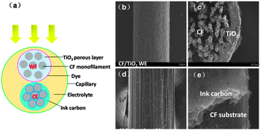 |
| | Fig. 1 (a) Schematic diagram of the all-carbon electrode-based fiber-shaped dye-sensitized solar cells. CF: carbon fiber; WE: working electrode; and CE: counter electrode. SEM top view (b) and cross-section view (c) of the CF/TiO2 photoanode. (d) Top view of the CF/ink all-carbon CE (C/CF CE). (e) The CF substrate and ink carbon layer of CE, where a boundary can be clearly seen. | |
The scanning electron microscope (SEM) images of the electrodes are shown in Fig. 1b–e. From the top-view SEM figure of the CF/TiO2 photoanode, the CF surface is evenly covered with TiO2 film (Fig. 1b). Under higher resolution (Fig. S2, ESI†), a porous and interconnected microstructure composed of anatase (Fig. S1, ESI†) TiO2 nanoparticles can be clearly seen. The cross-section image of the photoanode (Fig. 1c) reveals that the entire CF bundle substrate is covered with a TiO2 film of uniform thickness (approximately 20 μm). The surface of the inner CF monofilaments is also coated with a thin TiO2 film or irregular TiO2 particle clusters that can merge on the CF monofilaments (Fig. S2, ESI†), which is beneficial to an effective transfer of electrons between monofilaments and increases the light scattering effect on the CF surface to improve photon utilization. The loose connection of some monofilaments in Fig. 1c is mainly caused by shearing of the section during SEM sample preparation. The entire CF/TiO2 photoanode is a core–shell system. The thick TiO2 film shell is capable of effectively enriching dye molecules, harvesting light, and transporting electrons. The CF bundle substrate as the core has a larger specific area (BET test result is 2.38 m2 g−1) than common bulky materials, and its three-dimensional structure can form a radial collection field for an efficient carrier collection. Fig. 1d and e show the SEM images of the all-carbon CE. The electrode surface is uniformly coated with the ink carbon film. Under high resolution, the ink carbon film has a microporous structure and consists of nanoscale carbon particles (Fig. S2b, ESI†). Fig. 1e clearly shows the interface between the CF conductive substrate and the ink carbon catalyst layer.
Performance of the all-carbon CE
We firstly compared the performance of the fiber devices based on the CF/TiO2 photoanode and two different types of CEs: pure carbon fiber (CF CE) and carbon fiber/ink carbon CE (C/CF CE). As indicated by the J–V curves in Fig. 2(a), the efficiencies of the CF CE device (D1) and the C/CF CE device (D2) are 0.24% and 1.02% (DCF/TiO2, Table 1), respectively. The open circuit voltages (Voc) of the two devices are quite close (−0.27 V), but D1 has quite a low fill factor (FF) of only 0.17, and its short-circuit current density (Jsc) is also much lower (5.42 mA cm−2) than that of D2 (11.58 mA cm−2). Compared with D1, D2 has a much higher FF (up to 0.32). The difference in the performance is caused by the difference in the catalytic activities of CEs. Fig. 2b shows the electrochemical cyclic voltammetry (CV) curves of the two CEs in an acetonitrile solution containing 10 mM BMII, 1 mM I2, and 0.01 M LiClO4 as the supporting electrolyte. An AgCl/Ag electrode was used as the reference electrode. The pair of redox peaks (Pox/Pred) in the curves belong to the redox reaction of the I3−/I− couple.25 The size and shape of the peaks indicate the catalytic performance of the materials against the redox couples. Based on the CV curves in Fig. 2(b), the CF electrode does not show any apparent redox peaks, indicating its poor catalytic activity toward I3−/I−. One solution to improve the catalytic performance of materials was to increase the surface area. As powdered carbon nanofibers with large specific surface area have been used as an efficient CE catalyst in DSSCs. However, this kind of carbon nanofibers need to be ground and pasted on FTO with binder, which lose the many advantages of fibrous macromorphology, such as conductivity and self-standing ability.26 Here, an alternative strategy was presented, by using highly conductive and self-supporting carbon fiber as substrate directly, modifying its surface with highly catalytic ink to obtain the all-carbon CE (C/CF CE). The C/CF electrode shows apparent catalytic redox peaks and high redox current, suggesting that ink-coated CF can effectively catalyze the reduction of I3−. The good catalytic performance mainly resulted from the ink carbon particles with relatively large specific area (BET test result is 32.78 m2 g−1). Additionally, amorphous and nanoscaled ink particles have excellent catalytic activity toward I3−/I− and good adhesiveness to CF substrate (details about commercial ink as the surface modifier of CE were included in our ongoing paper).
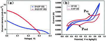 |
| | Fig. 2 (a) J–V curves of the fiber-shaped solar cells D1 and D2, using CF CE and C/CF CE respectively. (b) Cyclic voltammograms of the CF electrode (CF) and C/CF electrode at a scan rate of 50 mV s−1 in an acetonitrile solution containing 10 mM BMII, 1 mM I2, and 0.01 M LiClO4 as the supporting electrolyte. | |
Table 1 Parameters of the photovoltaic performances, electron transport properties, and dye-adsorption of the all-carbon electrode-based fiber-shaped DSSCs with (DCF/Ti/TiO2) or without (DCF/TiO2) titanium layer between CF and TiO2, and DSSCs with different CF/TiO2 photoanode diameters (95, 150, 250, 400 μm, respectively)
| Devices |
V
oc/V |
J
sc/mA cm−2 |
FF |
η (%) |
A
dye
/nmol cm−1 |
R
s/Ω cm2 |
R
re/Ω cm2 |
|
DCF/TiO2 |
0.271 |
11.58 |
0.323 |
1.02 |
/ |
/ |
/ |
|
DCF/Ti/TiO2 |
0.348 |
13.06 |
0.304 |
1.38 |
/ |
/ |
/ |
|
D-95 μm |
0.329 |
12.19 |
0.411 |
1.65 |
4.94 |
83.97 |
696.2 |
|
D-150 μm |
0.342 |
14.15 |
0.392 |
1.90 |
5.18 |
65.57 |
494.5 |
|
D-250 μm |
0.288 |
9.85 |
0.377 |
1.07 |
18.47 |
41.16 |
261.1 |
|
D-400 μm |
0.256 |
9.05 |
0.315 |
0.73 |
19.31 |
34.88 |
174.6 |
Interface engineering of the CF/TiO2 photoanode
The initial fiber-shaped DSSC based on an all-carbon electrode attained an efficiency of around 1%. This demonstrates the feasibility of producing efficient DSSCs from cheap all-carbon electrodes. However, the Voc of the proposed solar cell is quite low compared with traditional liquid DSSCs. As shown by inset (a) in Fig. 3, after photoexcitation of the dye molecules, electrons transit from the ground state to the excited state and are then injected into the conductive band (Ec) of the TiO2 semiconductor. The photoelectrons transport within the TiO2 film, pass through the CF/TiO2 interface, and are effectively collected by the conductive CF substrate. Voc is the difference between the fermi level (Ef) of the TiO2 semiconductor and the redox potential of the  couple in the electrolyte;27
| | 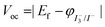 | (1) |
Assuming that the electrolyte in the system remains unchanged, Voc depends directly on the Ef of the TiO2 semiconductor. In an actual photoanode, when the CF substrate comes into direct contact with TiO2, the energy band of the TiO2 semiconductor bends (inset (b) in Fig. 3).28 Electrons overcome an interface barrier ΔEb1 when moving from the TiO2 to the CF substrate for collection. Given that the surface work function (Wf) of CF is much deeper than the Ec of TiO2, the contact between CF and TiO2 causes a negative shift in the Ef of the TiO2 semiconductor  and a reduction in Voc. Therefore, if the interface barrier of CF/TiO2 can be reduced, Voc as well as the device performance would be effectively enhanced.
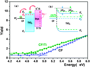 |
| | Fig. 3 Work function (Wf) curves of CF before and after magnetron sputtering of the Ti layer (CF/Ti), in which the energy threshold value (the cross point of the baseline and the sloped line) is equal to the Wf value. The measured Wf values for CF and CF/Ti are 4.95 and 4.67 eV, respectively. Inset (a) shows the relative position of the energy levels as well as the injection and transport of photogenerated electrons in the dye-sensitized CF/TiO2 photoanode. Inset (b) shows the energy band bending of the TiO2 semiconductor and the change in the fermi level without (CF) and with titanium layer (CF/Ti) between the CF substrate and the TiO2 semiconductor. | |
Based on the above analysis, we conducted a Ti magnetron sputtering on CF to regulate the CF/TiO2 interface barrier and prepared the DCF/Ti/TiO2 (with a Ti-sputtered layer). Compared with DCF/TiO2 (without Ti-sputtered layer), as shown in Table 1, DCF/Ti/TiO2 has a higher Jsc (13.06 mA cm−2), and its Voc increases to 348 mV, which is about 30% higher than that of DCF/TiO2, contributing to an efficiency of 1.38%, indicating that the interface engineering viaTi sputtering on the CF surface apparently improves the photovoltaic performance of the all-carbon electrode-based DSSC, which is in agreement with the previously mentioned theoretical prediction. Fig. 3 illustrates the change in Wf after Ti sputtering. The Wf of pure CF is determined as 4.95 eV, and it decreases to 4.67eV after Ti sputtering, subsequently causing changes in the interfacial properties between CF and TiO2. The fermi level of TiO2 semiconductor in this case  experienced a forward shift;
  , which is advantageous for higher Voc. Meanwhile, the barrier height at the interface between TiO2 and CF/Ti dropped from ΔEb1 to ΔEb2, further benefitting the injection of electrons from TiO2 to CF, as well as their transportation and collection, while passing through the energy barrier. By investigating the alternating current impedance of DCF/Ti/TiO2 and DCF/TiO2 (Fig. S3, ESI†), we have obtained the recombination resistance (Rre) at the TiO2/electrolyte interface. The Rre in DCF/Ti/TiO2 (655 Ω cm2) is much higher than that of DCF/TiO2 (248.6 Ω cm2), implying a reduced recombination for DCF/Ti/TiO2. The Ti-sputtered surface can be oxidized to a dense TiO2 layer, which is equivalent to the introduction of a TiO2 blocking layer between the CF substrate and TiO2 semiconductor. The TiO2 blocking layer can effectively inhibit the recombination of electrons in the TiO2 film or on the substrate surface with oxidative species in the electrolyte, resulting in better device performance.29
Effect of the photoanode diameter on device performance
Commercialized CF consists of monofilaments. A carbon-based photoanode employs commercialized CF bundles as conductive substrate. Thus, choosing CF bundles with different diameters to coat the TiO2 film for the preparation of photoanodes with different diameters is possible. The diameter of the CF bundle directly influences the conductivity of the electrode, the loading amount of TiO2 nanoparticles, and the apparent aperture area of the devices. Hence, the photoanode diameter greatly affects the device performance. We experimentally fabricated four photoanodes with different diameters (95, 150, 250, and 400 μm) and assembled the all-carbon electrode-based fiber-shaped DSSCs. The J–V characterization of these devices is displayed in Fig. 4a and the parameters are summarized in Table 1. As the diameter of the photoanode increases from 95 to 400 μm, the η of the corresponding device increases from 1.65% to the maximum and gradually decreases to the minimum (0.73%). In particular, FF gradually decreases from 0.41 to 0.32. Jsc and Voc experienced a trend similar to that of η, that is, initially increasing then decreasing (Fig. S4, ESI†). Therefore, an optimum performance of 14.15 mA cm−2, 342 mV, and 1.90% is achieved when the diameter is 150 μm. The trend of the parameters can be better understood through electrochemical impedance spectrum (EIS) analysis. Fig. 4b shows the Nyquist plots of the all-carbon electrode-based fiber DSSCs with photoanodes having different diameters via fitting with equivalent circuit (Fig. S4c, ESI†). When the diameter varies from 95 to 400 μm, the serial resistance (Rs) gradually decreases. A smaller Rs helps reduce the internal energy loss and increase the power output. On the other hand, as the TiO2 loading amount increases, the recombination sites inside the porous TiO2 film are also augmented. This is expressed by the apparent decrease in Rre at the TiO2 film/electrolyte interface along with the increase in diameter, implying a more serious recombination of electrons with oxidative species. Such a change in pattern of Rs and Rre results in a reduction in Voc and FF. The trend of Jsc can also be explained by the dye adsorption results. As the photoanode diameter increases, the TiO2 loading amount also increases, leading to greater enrichment of dye molecules (Table 1, Adye increases from 2.94 to 19.31 nmol cm−1). Ideally, the capture of photons and the improvement of photocurrent are favored. According to the formula| | 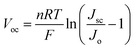 | (2) |
where Jo is the dark current density.30Voc improves as Jsc increases, but decreases as Jo increases. From the dark curves in Fig. 4a, Jo increases with increasing diameter, suggesting that a greater amount of recombination occurs, which is consistent with EIS results. Jsc and Jo work together to maximize Voc when the diameter is 150 μm. Although increasing the photoanode diameter can result in better dye-adsorption, the transmission distance of electrons (de) also increases to a certain extent. However, the effective electron diffusion length (Le) of the photoelectrons in the TiO2 film is limited. When de > Le, the recombination rate of the electrons significantly increases and disrupts the charge separation and collection. Therefore, choosing a suitable photoanode diameter will balance the cumulative effects of other factors to obtain an all-carbon electrode-based fiber DSSC with optimized performance. In addition, the EIS results (Table 1) show that the Rs values are much higher than that of the metal-based DSSC.14 This may be the primary reason for the low FF for all-carbon-based devices, suggesting that the device performance can be further improved if more conductive CFs are used.
 |
| | Fig. 4 (a) J–V curves of the fiber-shaped DSSCs based on CF/TiO2 photoanodes with different diameters under dark and light conditions. (b) EIS curves (Nyquist plots) of the fiber-shaped DSSCs based on the CF/TiO2 photoanode with different diameters. | |
We have also investigated the photocurrent response of the device, as illustrated in Fig. 5(a). In one cycle, the attenuation percentage of photocurrent is <4%. In the fifth cycle, the maximum photocurrent is roughly stabilized to approximately 95% of the initial maximum photocurrent. Within 60 s, the high photocurrent of the device shows remarkable reproducibility during on–off cycles. Another feature of the fiber-shaped solar cell is its three-dimensional light harvesting, enabling it to collect photons from different directions.14,15Fig. 5(b) shows the J–V curves under two irradiation modes, single-sided irradiation (SI, 100 mW cm−2) and double-sided irradiation (DI, same light source as SI, with a diffuse reflector at the bottom of the cell). Jsc is nearly doubled to 25.4 mA cm−2 and Voc increases by 40 mV after the diffuse reflector is added. This contributes to an apparent conversion efficiency of 3.4% of the DI device, indicating the potentially highly efficient energy output of fiber-shaped solar cells with all-carbon electrodes.
 |
| | Fig. 5 (a) Normalized photocurrent response (short-circuit current–time curve) of the all-carbon electrode-based fiber-shaped solar cell during light on–off cycles. (b) J–V curves of the all-carbon electrode-based fiber-shaped solar cells under two types of irradiation modes. SI represents the single-sided irradiation mode (standard light intensity of 100 mW cm−2), and the corresponding J–V curve is marked with blue solid triangles. DI represents the double-sided irradiation mode with a diffuse reflector at the bottom of the device, and the corresponding J–V curve is marked with red solid circles. | |
One prominent advantage of the all-carbon electrode-based fiber-shaped DSSC is the absence of TCOs or expensive electrode materials. Instead, abundant, highly stable and biocompatible carbon materials have been adopted. It has successfully realized the application of all-carbon electrodes in DSSCs and it is also the first reported efficient DSSC based on an all-carbon electrode to our knowledge. Carbon-based photoanodes capable of efficient light harvesting, along with effective injection and collection of carriers, function synergistically with the highly catalytic all-carbon CE to obtain high photocurrent. When the Voc and FF are quite low, the device can still gain a remarkable power conversion efficiency, which is much higher than those of previously reported DSSCs with carbon nanotube scaffolds or carbon nanofiber-based photoanodes.23,24 A considerable improvement in Voc can be achieved by further interface modification or using other carbon substrates with lower Wf (such as graphene or semiconductive carbon nanotubes, among others), reducing the defects in the semiconductive film to reduce recombination. A higher FF is expected by optimizing the film preparation process and electrolytic composition or by using more conductive carbon materials as substrates. Thus, the photovoltaic performance of the all-carbon electrode-based DSSC still has plenty of room for improvement.
Conclusions
In summary, we have developed a novel all-carbon electrode-based fiber-shaped DSSC, in which the core–shell structured CF/TiO2 photoanode and the CF/ink all-carbon CE are prepared via simple processes. The ηmax of the devices under 100 mW cm−2 illumination reaches 1.9%. Both electrodes use low-cost carbon materials, resulting in highly cost-effective solar cells. Notably, the design of the all-carbon electrodes can be extended to other photovoltaic systems, such as quantum dots and organic solar cells. The all-carbon electrode-based fiber cells also have potential applications in woven electronics because of the flexibility of the CF substrates.31 Moreover, ultralow-cost and bio-friendly all-carbon-based DSSCs can be achieved for large-scale production with the use of organic dyes and organic electrolytes.
Acknowledgements
The current work is jointly supported by the NSFC (No. 50833001), MOST (No. 2011CB933300), and MOE (No. 309001) of China.
Notes and references
- B. Oregan and M. Gratzel, Nature, 1991, 353, 737 CrossRef CAS.
- M. K. Nazeeruddin, A. Kay, I. Rodicio, R. Humphrybaker, E. Muller, P. Liska, N. Vlachopoulos and M. Gratzel, J. Am. Chem. Soc., 1993, 115, 6382 CrossRef CAS.
- Q. J. Yu, Y. H. Wang, Z. H. Yi, N. N. Zu, J. Zhang, M. Zhang and P. Wang, ACS Nano, 2010, 4, 6032 CrossRef CAS.
- F. Gao, Y. Wang, D. Shi, J. Zhang, M. K. Wang, X. Y. Jing, R. Humphry-Baker, P. Wang, S. M. Zakeeruddin and M. Gratzel, J. Am. Chem. Soc., 2008, 130, 10720 CrossRef CAS.
- K. Okada, H. Matsui, T. Kawashima, T. Ezure and N. Tanabe, J. Photochem. Photobiol., A, 2004, 164, 193 CrossRef CAS.
- M. G. Kang, N. G. Park, K. S. Ryu, S. H. Chang and K. J. Kim, Sol. Energy Mater. Sol. Cells, 2006, 90, 574 CrossRef CAS.
- S. Ito, N. L. C. Ha, G. Rothenberger, P. Liska, P. Comte, S. M. Zakeeruddin, P. Pechy, M. K. Nazeeruddin and M. Gratzel, Chem. Commun., 2006, 4004 RSC.
- X. Fan, F. Z. Wang, Z. Z. Chu, L. Chen, C. Zhang and D. C. Zou, Appl. Phys. Lett., 2007, 90, 073501 CrossRef.
- Y. H. Wang, H. X. Yang, Y. Liu, H. Wang, H. Shen, J. Yan and H. M. Xu, Prog. Photovoltaics., 2010, 18, 285 CAS.
- J. W. Liu, M. A. G. Namboothiry and D. L. Carroll, Appl. Phys. Lett., 2007, 90, 063501 CrossRef.
- X. Fan, Z. Z. Chu, F. Z. Wang, C. Zhang, L. Chen, Y. W. Tang and D. C. Zou, Adv. Mater., 2008, 20, 592 CrossRef CAS.
- M. R. Lee, R. D. Eckert, K. Forberich, G. Dennler, C. J. Brabec and R. A. Gaudiana, Science, 2009, 324, 232 CrossRef CAS.
- B. Weintraub, Y. G. Wei and Z. L. Wang, Angew. Chem., Int. Ed., 2009, 48, 8981 CrossRef CAS.
- Z. B. Lv, Y. P. Fu, S. C. Hou, D. Wang, H. W. Wu, C. Zhang, Z. Z. Chu and D. C. Zou, Phys. Chem. Chem. Phys., 2011, 13, 10076 RSC.
- Y. P. Fu, Z. B. Lv, S. C. Hou, H. W. Wu, D. Wang, C. Zhang, Z. Z. Chu, X. Cai, X. Fan, Z. L. Wang and D. C. Zou, Energy Environ. Sci., 2011, 4, 3379 Search PubMed.
- G. Girishkumar, K. Vinodgopal and P. V. Kamat, J. Phys. Chem. B, 2004, 108, 19960 CrossRef CAS.
- K. Ozawa, Solid State Ionics, 1994, 69, 212 CrossRef CAS.
- G. Li, V. Shrotriya, J. S. Huang, Y. Yao, T. Moriarty, K. Emery and Y. Yang, Nat. Mater., 2005, 4, 864 CrossRef CAS.
- A. Kay and M. Gratzel, Sol. Energy Mater. Sol. Cells, 1996, 44, 99 CrossRef CAS.
- K. Imoto, K. Takahashi, T. Yamaguchi, T. Komura, J. Nakamura and K. Murata, Sol. Energy Mater. Sol. Cells, 2003, 79, 459 CrossRef CAS.
- M. X. Wu, X. Lin, T. H. Wang, J. S. Qiu and T. L. Ma, Energy Environ. Sci., 2011, 4, 2308 CAS.
- P. Brown, K. Takechi and P. V. Kamat, J. Phys. Chem. C, 2008, 112, 4776 CAS.
- H. E. Unalan, D. Wei, K. Suzuki, S. Dalal, P. Hiralal, H. Matsumoto, S. Imaizumi, M. Minagawa, A. Tanioka, A. J. Flewitt, W. I. Milne and G. A. J. Amaratunga, Appl. Phys. Lett., 2008, 93, 133116 CrossRef.
- J. W. Liu, Y. T. Kuo, K. J. Klabunde, C. Rochford, J. Wu and J. Li, ACS Appl. Mater. Interfaces, 2009, 1, 1645 CAS.
- J. D. Roy-Mayhew, D. J. Bozym, C. Punckt and I. A. Aksay, ACS Nano, 2010, 4, 6203 CrossRef CAS.
- P. Joshi, L. F. Zhang, Q. L. Chen, D. Galipeau, H. Fong and Q. Q. Qiao, ACS Appl. Mater. Interfaces, 2010, 2, 3572 CAS.
- A. J. Frank, N. Kopidakis and J. van de Lagemaat, Coord. Chem. Rev., 2004, 248, 1165 CrossRef CAS.
- H. Ishii, H. Oji, E. Ito, N. Hayashi, D. Yoshimura and K. Seki, J. Lumin., 2000, 87–89, 61–65 CrossRef CAS.
- P. J. Cameron and L. M. Peter, J. Phys. Chem. B, 2003, 107, 14394 CrossRef CAS.
- M. Gratzel, J. Photochem. Photobiol., A, 2004, 168, 235 CrossRef.
- R. F. Service, Science, 2003, 301, 909 CrossRef CAS.
Footnotes |
| † Electronic supplementary information (ESI) available. See DOI: 10.1039/c1cp22613d. |
| ‡ These authors contributed equally to this work. |
|
| This journal is © the Owner Societies 2012 |
Click here to see how this site uses Cookies. View our privacy policy here.