DOI:
10.1039/C1CE06107K
(Communication)
CrystEngComm, 2012,
14, 53-58
Growth and properties of single-crystalline Ge nanowires and germanide/Ge nano-heterostructures†
Received
28th August 2011
, Accepted 7th October 2011
First published on 2nd November 2011
Abstract
Single-crystalline Ge nanowires have been synthesized on Au-coated Si substrates through a thermal evaporation, condensation method and vapor–liquid–solid mechanism. The [111] growth direction of the Ge nanowires was analyzed using HRTEM and fast Fourier transform diffraction patterns. Global back-gated Ge nanowire field-effect transistors (FETs) on the Si3N4 dielectrics were fabricated and studied, showing p-type behavior and a field effect hole mobility of 44.3 cm2 V−1 s−1. The Ge channel length could be well controlled through the annealing process. After a rapid thermal annealing (RTA) process, Ni2Ge/Ge/Ni2Ge nano-heterostructures were formed. The electrical transport properties were effectively improved by the heterojunction rather than the metal contact. The epitaxial relationship between Ge and orthorhombic Ni2Ge was Ge[110]//Ni2Ge[110] and Ge(-11-1)//Ni2Ge(1-1-2). From electrical transport properties, the measured resistivity of the Ge nanowires was much lower than intrinsic bulk Ge material. A room temperature photoluminescence spectrum of the Ge nanowires possessed a broad blue emission with a peak at 462 nm in wavelength, which was attributed to the oxide-related defect states. Due to the existence of the defects, a Ge nanowire FET was able to detect visible light and serve as a nanowire photodetector.
Introduction
Following Moore's law, the gate length of an FET transistor in an integrated circuit keeps downscaling. The controllable synthesis of nanostructures is regarded as a potential solution to break through the bottleneck of photolithography. Owning to quantum size effects and surface effects due to the structural uniqueness and the ultrahigh surface-to-volume ratio of nanostructures, nanowires have attracted considerable attention and been applied in a wide range of nanodevices, including FETs,1 logic gates,2 chemical sensors,3 solar cells4,5 and photodetectors6,7etc. Among semiconductor nanowires, group IV materials such as Si and Ge are used as potential materials that can be integrated with conventional Si-based technology. Compared with Si, carrier mobility and exciton Bohr radius are higher in Ge,8 contributing to prominent physical properties such as the quantum confinement effect. Therefore, Ge nanowires were considered a promising transistor channel material. However, due to Fermi level pinning between metal and semiconductor, a Schottky barrier exists at the contact and induces large contact resistance.9 The Schottky contact would limit the performance of the nanowire device. To solve this problem, considerable work has demonstrated that the formation of silicide/Si heterostructures could effectively avoid the Fermi level pinning effect.10–13 Therefore, the heterojunction of germanide and Ge might suggest an effective method to improve the electrical transport properties. Compared with silicide/Si heterostructures, little research has been performed on germanide/Ge heterostructures.14,15 In addition, in situtransmission electron microscopy (TEM)16–26 was utilized to study the kinetics of the reaction and the growth mechanism of the nano-heterostructures of single crystal Ni2Ge/Ge in a Ge nanowire is proposed. The Schottky barrier height of the Ni2Ge/Ge interface is about 0.2 eV, which is so small that the interface has the potential of being an ohmic contact.
In this work, single-crystalline Ge nanowires were synthesized. Furthermore, germanide/Ge/germanide heterostructures were formed through solid state reaction between Ni contacts and Ge nanowires. The Ge channel length can be well controlled through multiple annealing processes. The epitaxial relationship between Ge and orthorhombic Ni2Ge was analyzed. Additionally, the electrical transport and optical properties of the Ge nanowires and Ni2Ge/Ge/Ni2Ge nano-heterostructures were also measured and discussed.
Experimental methods
Single-crystalline Ge nanowires were synthesized in a horizontal tube furnace through thermal evaporation, as shown in Fig. 1. A quartz tube with a diameter of 2 in was mounted in the furnace. An alumina crucible containing Ge powder was placed in the high temperature (950 °C) zone. A 4 cm2Si(100) wafer coating with 3 nm Au film was placed in the low temperature (550 °C) zone. The chamber was evacuated to 10−2 Torr then the pressure was adjusted through the control of the butterfly valve linked to the pump and the pressure maintained at 15 Torr, with Ar and H2 maintained at 30 and 10 sccm, respectively. The temperature was held for 1 h after reaching the set value. To investigate the electron transport properties, Ge nanowires were suspended in ethanol and positioned on a Si3N4/Si substrate. The Si3N4 layer, with thickness of 300 nm, was grown through low temperature chemical vapor deposition and served as a dielectric layer. A heavily doped Si substrate was used as a back gate. Ni pad definition was carried out through e-beam lithography, metal deposition and lift-off. After rapid thermal annealing at 350 °C, a germanide/Ge heterojunction was formed. The morphology and structure of the nanowires were investigated using a JEOL 6700 scanning electron microscope (SEM) and a JEOL 2100F high resolution transmission electron microscope (HRTEM). The electrical transport properties and photoluminescence (PL) spectra were measured using an Agilent B1500A and a HORIBA iHR320 imaging spectrometer, respectively. A laser of 10 mW at a wavelength of 532 nm was used as the light source for photosensing property investigations. All measurements were performed at room temperature in ambient conditions.
Results and discussion
Heterostructure formation and germanide characterization
Ni served as the electrical contact and the pad was defined through e-beam lithography. Before nickel deposition, the sample was dipped into BOE for 30 s to fully eliminate oxide at a defined region. The contact was accomplished after Ni deposition and lift-off. The black line in Fig. 2(a) shows the electrical characteristics of the device. After RTA at 350 °C for 5 min, the electrical transport curve (red line) implied that the Schottky barrier was effectively decreased with an order of magnitude decrease in resistance. The workfunction of Ni2Ge is 4.86 eV, which is 0.2 eV lower than the valence band of Ge.15 The small barrier conformed to the ohmic current–voltage curve measured after annealing treatment. With different contrast under SEM observation, as shown in Fig. 2(b), it was clear that the Ni contact reacted with the Ge nanowires and a germanide/Ge/germanide nano-heterostructure could be clearly observed.
 |
| | Fig. 2 (a) Current–voltage curves measured before and after RTA treatment, respectively. Conductivity was effectively enhanced after the annealing process. (b) SEM image of a germanide/Ge/germanide heterostructure nanowire. | |
To investigate the structures of germanide and Ge, the device was fabricated on the TEM specimen with a square window covered with a glassy, 60 nm thick Si3N4 film. After annealing treatment, the Ni contact reacted with the Ge nanowires and germanide/Ge/germanide heterostructures formed. Due to volume expansion, germanide distorted the morphology. In Fig. 3(a), a sharp interface between germanide and Ge is observed. Orthorhombic Ni2Ge and diamond cubic Ge were analyzed using HRTEM imaging and fast Fourier transform (FFT) in Fig. 3(b), respectively. The Ni2Ge was identified to be orthorhombic with lattice constants of a = 0.511 nm, b = 0.383 nm, c = 0.726 nm and Ge was identified to be of diamond cubic crystal structure grown along the [111] direction. The epitaxial relationship between Ge and Ni2Ge was Ge[110]//Ni2Ge[110] and Ge(−11−1)//Ni2Ge(1−1−2). The lattice mismatch between Ge(−11−1) and Ni2Ge(1−1−2) is about 25%. In Fig. 3(c), a dislocation is observed at the heterojunction with a Burgers vector of [1−11]. It was speculated that the dislocations formed in order to relax the strain induced by large lattice mismatch.
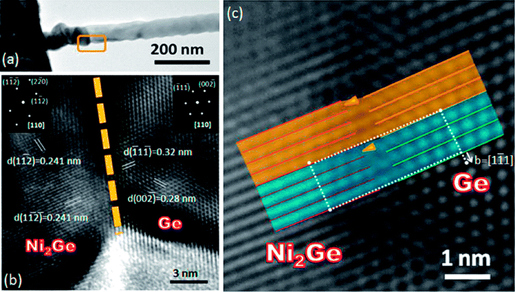 |
| | Fig. 3 (a) Low magnification TEM image showing the sharp interface of the germanide/Ge heterojunction. (b) HRTEM image of a Ni2Ge/Ge heterojunction. The insets show the FFT patterns of Ni2Ge and Ge, respectively. (c) HRTEM image of a Ni2Ge/Ge heterojunction. The arrows indicate the dislocations induced by large lattice mismatch. | |
Multiple RTA and measurement
To understand the annealing process, multiple RTA was performed on the device to control the channel length and investigate the relationship between electrical transport properties and annealing treatment. After multiple RTA treatments, the channel length shrank from 4.46 μm to 3.42 μm, as shown in Fig. 4(a). The RTA furnace ramped to 350 °C at a rate of 30 °C s−1 and keeps for 3 min at every step. In addition, the growth process of the germanide was also observed through in situTEM observation (ESI Movie 1†). When the germanide/Ge heterojunction had formed, ohmic contact behavior was observed (Fig. 4(b)). The calculated resistance of the nanowires after each annealing treatment as a function of channel length is shown in Fig. 4(c). The 2nd, 3rd and 4th data exhibited a linear relationship and fit in with R = ρL/A, where R, ρ, L and A represent resistance, resistivity, channel length and cross-section area of the nanowires, respectively. From the extrapolation of this linear relation, 18.86 MΩ could be obtained at a channel length of 4.46 μm with ohmic contact. The resistance measured at a channel length of 4.46 μm was 73.75 MΩ, which was four times larger than the extrapolated data, whereas 672 MΩ was measured before annealing treatment. Compared with the data before RTA treatment, the resistance was decreased about an order after the 1st RTA. We speculate that only part of the cross-section formed germanide after the 1st annealing treatment. Due to the limited carrier injection area, the contact resistance was not completely reduced by the annealing treatment. After further annealing, the electron transport properties could be enhanced through the larger carrier injection area.27
 |
| | Fig. 4 (a) SEM images after multiple annealing treatments. After 4 annealing steps, the channel length shrank from 4.46 μm to 3.42 μm. (b) Current–voltage curves measured after each annealing treatment. (c) Plot of resistance as a function of channel length. The inset shows a schematic illustration of partially formed germanide. | |
Furthermore, resistivity extracted from the linear relation is 0.579 Ω cm, which is nearly two orders lower than the intrinsic value for the commercial bulk wafer (47 Ω cm). The reduction of resistivity could be attributed to the native oxide layers on the Ge nanowires since there was no intentional doping of the nanowires. There were surface states existing at the interface between the oxide layers and Ge nanowires.28,29 The electrons in the Ge nanowires would be captured by surface states, inducing surface hole accumulation. Thus the conductivity of the nanowires follows in direct proportion to the concentration of the nanowires as in eqn (1):30
where
n0,
ns,
d and
μh represent intrinsic carrier concentration, surface concentration induced by surface hole accumulation, diameter of
nanowires and hole mobility, respectively. Given the large surface to volume ratio of the
nanowires, the dimension should play an important role in electrical transport properties. It is suggested that the surface concentration induced by hole accumulation is attributed to the improvement of conductivity, in other words, the reduction of resistivity.
FET
To study the electrical transport properties of the Ni2Ge/Ge/Ni2Ge heterostructures, global back-gate field-effect transistors were fabricated on the Si3N4 dielectric, followed by rapid thermal annealing at 350 °C for 5 min. The output and transfer characteristics of the Ni2Ge/Ge/Ni2Ge nanowires were measured. Fig. 5(a) shows the characteristics of a p-channel transistor. Although the Ge nanowires were not intentionally doped, the transistor exhibited p-type semiconducting behavior. A similar phenomenon was also discovered in a Si nanowire.31 The p-channel characteristics can be attributed to the hole accumulation induced by surface states. The Id–Vg double sweep curve exhibited a hysteresis loop which is related to surface states, as shown in Fig. 5(b). The energy band structure at the surface of a nanowire is related to the adjustment of gate voltage. When a negative gate voltage is applied, the electron captured by the lower surface state level will be neutralized by holes accumulated at the surface of the nanowire. On the contrary, when a positive gate voltage is applied, the lower surface state level will be charged by an electron. However, the charge redistribution is a slow process which is limited by a diffusion barrier or a tunneling barrier at the surface of the nanowire. The existence of the hysteresis loop also proved the existence of the surface states which trapped charges and induced slow charge redistribution. To estimate the field effect hole mobility, characteristic measurements were carried out. In Fig. 5(c), the capacitance was calculated and based on the cylinder-on-plate model. In eqn (2):| |  | (2) |
where εnitride is the dielectric constant of Si3N4 (εnitride = 7.5), ε0 = 8.85 × 10⁻¹² F m−1, L is the length of the Ge channel, r is the radius of the nanowire, and tnitride is the thickness of the dielectric layer; the capacitance is about 0.48 fF for L = 2.55 μm, r = 86 nm and tnitride = 300 nm, respectively. The field effect hole mobility can be calculated using eqn (3):| |  | (3) |
where μ, Cnitride and gm are carrier mobility, nitride capacitance and transconductance, respectively. Then gm = 1.6 × 10⁻⁸ was extracted from the linear region of the Id–Vg curves at a bias voltage of 50 mV and the carrier mobility was estimated to be about 44.3 cm2 V−1 s−1.
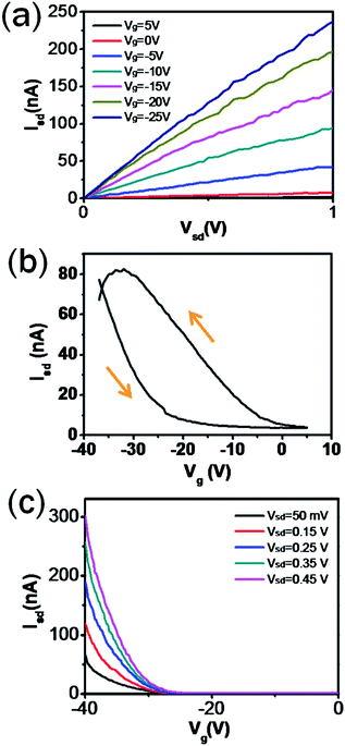 |
| | Fig. 5 Electrical characteristics of a Ni2Ge/Ge/Ni2Ge nanowire FET. (a) Id–Vd curves of a back-gate nanowire transistor. (b) Id–Vg double sweep exhibiting a hysteresis loop. (c) Id–Vg curves of a back-gate nanowire transistor. | |
The cylinder-on-plate model assumed that the nanowire was embedded in the dielectrics and possessed a circular cross-section. In reality, the nanowire was deposited on the top of the dielectric layer. Therefore, the nanowire was not completely wrapped by dielectric; the value of capacitance obtained through the cylinder-on-plate model was the upper limit in this case. On the other hand, the surface states induced by the oxide will lower the total capacitance, thus the mobility will be underestimated.32
Optical properties
Fig. 6(a) shows the room temperature PL spectrum of the as-grown Ge nanowires. The PL spectrum possesses a broad blue emission with a peak at 462 nm in wavelength, which was attributed to the oxide related defect states.33–36 Based on the results of the PL measurements, a laser of 10 mW at a wavelength of 532 nm was used as the light source to investigate the photosensing properties of Ni2Ge/Ge/Ni2Ge nanowires which were formed after annealing at 350 °C for 5 min. The device was illuminated under processing of the current–voltage measurements. In Fig. 6(b), the conductivity was promoted from 3.19 nS to 28.32 nS under illumination. It was speculated that the defect states were excited and the carrier concentration was massively raised. From the current–time measurements in Fig. 6(c), two photoresponse behaviors can be clearly observed. The fast and slow responses resulted from electron–hole recombination and electron relaxation of the surface states, respectively.28 Due to the existence of oxide defects, Ge nanowires will be a promising candidate material for visible light detection.
 |
| | Fig. 6 Optical properties of Ni2Ge/Ge/Ni2Ge heterostructure nanowires. (a) PL spectrum of the as-grown Ge nanowires. (b) Current–voltage curves measured without a light source and under light illumination, respectively. (c) Photoresponse measurement of a Ni2Ge/Ge/Ni2Ge nanodevice. | |
Conclusions
Single-crystalline Ge nanowires were synthesized via a thermal evaporation and condensation method. A single Ge nanowire field effect transistor has been fabricated through e-beam lithography, metal deposition and a lift-off process. Germanide/Ge heterostructures were formed by a rapid thermal annealing process. Orthorhombic Ni2Ge and diamond cubic Ge exhibit an epitaxial relationship of Ge[110]//Ni2Ge[110] and Ge(−11−1)//Ni2Ge(1−1−2). Ge channel length could be controlled through the multiple annealing processes. The formation of the heterojunction could avoid the Fermi level pinning effect. The performance of the electrical properties was also affected by the carrier injection area. Owing to surface hole accumulation, intrinsic Ge nanowires exhibited p-type semiconducting behavior with a field effect hole mobility of 44.3 cm2 V−1 s−1. Additionally, Ni2Ge/Ge/Ni2Ge nanowires are promising for visible light detection.
Acknowledgements
The authors would like to acknowledge the support of the ROC National Science Council through Grant Nos. NSC NSC 100-2628-E-009-023-MY3, and NSC 100-2120-M-007-008.
Notes and references
- L. Zhang, R. Tu and H. Dai, Nano Lett., 2006, 6, 2785–2789 CrossRef CAS.
- Y. Huang, X. F. Duan, Y. Cui, L. J. Lauhon, K. H. Kim and C. M. Lieber, Science, 2001, 294, 1313–1317 CrossRef CAS.
- Y. Cui, Q. Q. Wei, H. K. Park and C. M. Lieber, Science, 2001, 293, 1289–1292 CrossRef CAS.
- K. Q. Peng, Y. Xu, Y. Wu, Y. J. Yan, S. T. Lee and J. Zhu, Small, 2005, 1, 1062–1067 CrossRef CAS.
- B. Z. Tian, X. L. Zheng, T. J. Kempa, Y. Fang, N. F. Yu, G. H. Yu, J. L. Huang and C. M. Lieber, Nature, 2007, 449, 885–890 CrossRef CAS.
- Y. H. Ahn and J. Park, Appl. Phys. Lett., 2007, 91, 162102 CrossRef.
- C. J. Kim, H. S. Lee, Y. J. Cho, K. Kang and M. H. Jo, Nano Lett., 2010, 10, 2043–2048 CrossRef CAS.
- B. Yu, X. H. Sun, G. A. Calebotta, G. R. Dholakia and M. Meyyappan, J. Cluster Sci., 2006, 17, 579–597 CrossRef CAS.
- K. Yamane, K. Hamaya, Y. Ando, Y. Enomoto, K. Yamamoto, T. Sadoh and M. Miyao, Appl. Phys. Lett., 2010, 96, 162104 CrossRef.
- W. M. Weber, L. Geelhaar, A. P. Graham, E. Unger, G. S. Duesberg, M. Liebau, W. Pamler, C. Cheze, H. Riechert, P. Lugli and F. Kreupl, Nano Lett., 2006, 6, 2660–2666 CrossRef CAS.
- Y. C. Lin, K. C. Lu, W. W. Wu, J. W. Bai, L. J. Chen, K. N. Tu and Y. Huang, Nano Lett., 2008, 8, 913–918 CrossRef CAS.
- W. W. Wu, K. C. Lu, C. W. Wang, H. Y. Hsieh, S. Y. Chen, Y. C. Chou, S. Y. Yu, L. J. Chen and K. N. Tu, Nano Lett., 2010, 10, 3984–3989 CrossRef CAS.
- A. L. Schmitt, J. M. Higgins, J. R. Szczech and S. Jin, J. Mater. Chem., 2010, 20, 223–235 RSC.
- N. S. Dellas, S. Minassian, J. M. Redwing and S. E. Mohney, Appl. Phys. Lett., 2010, 97, 263116 CrossRef.
- J. S. Tang, C. Y. Wang, F. X. Xiu, A. J. Hong, S. Y. Chen, M. S. Wang, C. F. Zeng, H. J. Yang, H. Y. Tuan, C. J. Tsai, L. J. Chen and K. L. Wang, Nanotechnology, 2010, 21, 505704 CrossRef.
- E. A. Stach, P. J. Pauzauskie, T. Kuykendall, J. Goldberger, R. He and P. Yang, Nano Lett., 2003, 3, 867–869 CrossRef CAS.
- D. Golberg, Y. B. Li, M. Mitome and Y. Bando, Chem. Phys. Lett., 2005, 409, 75–80 CrossRef CAS.
- C. Lang, S. Kodambaka, F. M. Ross and D. J. H. Cockayne, Phys. Rev. Lett., 2006, 97, 226104 CrossRef CAS.
- C. H. Liu, W. W. Wu and L. J. Chen, Appl. Phys. Lett., 2006, 88, 133112 CrossRef.
- H. C. Hsu, W. W. Wu, H. F. Hsu and L. J. Chen, Nano Lett., 2007, 7, 885–889 CrossRef CAS.
- K. C. Lu, K. N. Tu, W. W. Wu, L. J. Chen, B. Y. Yoo and N. V. Myung, Appl. Phys. Lett., 2007, 90, 253111 CrossRef.
- K. C. Lu, W. W. Wu, H. W. Wu, C. M. Tanner, J. P. Chang, L. J. Chen and K. N. Tu, Nano Lett., 2007, 7, 2389–2394 CrossRef CAS.
- K. C. Chen, W. W. Wu, C. N. Liao, L. J. Chen and K. N. Tu, Science, 2008, 321, 1066–1069 CrossRef CAS.
- Y. C. Chou, W. W. Wu, S. L. Cheng, B. Y. Yoo, N. Myung, L. J. Chen and K. N. Tu, Nano Lett., 2008, 8, 2194–2199 CrossRef CAS.
- Y. C. Chou, W. W. Wu, L. J. Chen and K. N. Tu, Nano Lett., 2009, 9, 2337–2342 CrossRef CAS.
- K. C. Lu, W. W. Wu, H. Ouyang, Y. C. Lin, Y. Huang, C. W. Wang, Z. W. Wu, C. W. Huang, L. J. Chen and K. N. Tu, Nano Lett., 2011, 11, 2753–2758 CrossRef CAS.
- E. S. Liu, N. Jain, K. M. Varahramyan, J. Nah, S. K. Banerjee and E. Tutuc, IEEE Trans. Nanotechnol., 2010, 9, 237–242 CrossRef.
- T. Hanrath and B. A. Korgel, J. Phys. Chem. B, 2005, 109, 5518–5524 CrossRef CAS.
- D. W. Wang, Y. L. Chang, Q. Wang, J. Cao, D. B. Farmer, R. G. Gordon and H. J. Dai, J. Am. Chem. Soc., 2004, 126, 11602–11611 CrossRef CAS.
- J. S. Jie, W. J. Zhang, K. Q. Peng, G. D. Yuan, C. S. Lee and S. T. Lee, Adv. Funct. Mater., 2008, 18, 3251–3257 CrossRef CAS.
- C. M. Lieber, Y. Cui, X. F. Duan and J. T. Hu, J. Phys. Chem. B, 2000, 104, 5213–5216 Search PubMed.
- B. Yoo, A. Dodabalapur, D. C. Lee, T. Hanrath and B. A. Korgel, Appl. Phys. Lett., 2007, 90, 072106 CrossRef.
- S. Miyazaki, K. Sakamoto, K. Shiba and M. Hirose, Thin Solid Films, 1995, 255, 99–102 CrossRef CAS.
- S. Sato, S. Nozaki, H. Morisaki and M. Iwase, Appl. Phys. Lett., 1995, 66, 3176–3178 CrossRef CAS.
- K. Das, A. K. Chakraborty, M. L. NandaGoswami, R. K. Shingha, A. Dhar, K. S. Coleman and S. K. Ray, J. Appl. Phys., 2007, 101, 074307 CrossRef.
- L. Z. Pei, H. S. Zhao, W. Tan, H. Y. Yu, Y. W. Chen, C. G. Fan and Q. F. Zhang, Mater. Charact., 2009, 60, 1400–1405 CrossRef CAS.
Footnote |
| † Electronic supplementary information (ESI) available: Supplementary movie 1: an in situTEM video presenting dynamic observation of the Ni2Ge/Ge/Ni2Ge nanowire heterostructure formation and illustrating our study of the growth kinetics, taken at 350 °C and in a vacuum better than 10−7 Torr. See DOI: 10.1039/c1ce06107k |
|
| This journal is © The Royal Society of Chemistry 2012 |
Click here to see how this site uses Cookies. View our privacy policy here. 