Semiconductor monolayer assemblies with oriented crystal faces†
Guijun
Ma
ab,
Tsuyoshi
Takata
a,
Masao
Katayama
a,
Fuxiang
Zhang
a,
Yosuke
Moriya
a,
Kazuhiro
Takanabe
b,
Jun
Kubota
a and
Kazunari
Domen
*a
aDepartment of Chemical System Engineering, The University of Tokyo, 7-3-1 Hongo, Bunkyo-ku, Tokyo, 113-8656, Japan. E-mail: domen@chemsys.t.u-tokyo.ac.jp; Fax: +81-3-5841-8838; Tel: +81-3-5841-1148
bKAUST Catalysis Center, King Abdullah University of Science and Technology (KAUST), 4700 KAUST, Thuwal, 23955-6900, Saudi Arabia
First published on 16th November 2011
Abstract
Fabrication of two-dimensional monolayers of crystalline oxide and oxynitride particles was attempted on glass plate substrates. X-Ray diffraction patterns of the assemblies show only specific crystal facets, indicative of the uniform orientation of the particles on the substrate. The selectivity afforded by this immobilization technique enables the organization of randomly distributed polycrystalline powders in a controlled manner.
Recent advances in crystalline materials have enabled us to investigate the function of individual crystal planes among multiple crystal facets.1–8 It remains challenging to prepare crystals with a large area of a selected crystal facet exposed, because the interfacial energy and growth rate during the crystal growth process are anisotropic.9 Selectively exposed facets are currently fabricated by mechanical slicing of single crystals, but this technology lacks scalability.10 It would be of interest for both the industry and academia to develop a technique for selecting preferred crystal faces from randomly dispersed polycrystalline powders.
It is quite feasible to synthesize a variety of highly crystalline particulates with anisotropic crystal facets.2–8,11 The particle size can be tuned from several hundred nanometres to micrometres. Inorganic surfaces with specific facets have been used in surface science, crystallography, catalysis, etc.2–8 Recently, it has been shown that the photocatalytic activity of inorganic crystalline materials depends on the surface facet.5–8 Therefore, selective modification of crystalline facets on catalyst surfaces is of great interest, requiring special particle arrangements on the exposed target facets.
It is possible to immobilize micron-sized particulates into two-dimensional arrays on flat substrates.12–16 Riman et al.13 reported the self-assembly of a lead zirconium titanate microcrystal monolayer containing preferentially oriented arrays of crystal faces, and defined the structure as a “single-crystal-like” material. Tsapatsis's group14 coated hexagonal ZSM-2 nanoplates onto flat substrates by a convective assembly technique, which showed a slight orienting effect of crystal faces. With the exception of the above examples of particle layers, little attention has been paid to the orientation of crystal faces. To the best of our knowledge, there has been no report on assemblies of semiconductor monolayers with oriented crystal faces, which are expected to have a potential use in photonic materials, optoelectronic devices, and photochemical and biochemical sensors.
In the present study, monolayer assemblies are fabricated using oxide (TiO2, SrTiO3, ZnO) and oxynitride (LaTiO2N, BaTaO2N) powders as target deposition materials. Immobilization is achieved by molecular linkers, whose functional groups form chemical bonds between the particles and the substrate (glass plate (GP) in this study). Yoon's group15,16 reported the successful preparation of monolayers on different substrates using two-functional-group carbosilanes as interconnecting molecular linkages between microcrystal zeolites and a substrate. Their method exploits the abundant hydroxyl groups on the zeolite crystal surfaces to react and bind with the carbosilane linkers. Since the hydroxyl ion is a common surface functional group in oxygen-containing materials, the present study employed Yoon's preparation procedure16 to fabricate the oxide and oxynitride monolayers. The target materials selected were TiO2 (rutile), SrTiO3, ZnO, BaTaO2N and LaTiO2N, which are known semiconductor photocatalysts.17
TiO2 (rutile), SrTiO3 and ZnO were used as-purchased, and BaTaO2N and LaTiO2N were synthesized by the present author's group (see experimental details in the ESI†). The process of tethering semiconductor particles on a GP (a standard 19 × 13 × 1 mm glass plate) is illustrated in Scheme 1. To bind the oxide/oxynitride particles and GP, 3-iodopropyltrimethoxysilane (IP-TMS, Sigma-Aldrich, 95%) was used as a molecular linker. Toluene was used as a solvent to form a non-aqueous environment. The reflux process proceeded through reactions between the hydroxyl groups of the GP and the methoxy groups of IP-TMS, while the ultrasonication process employed reactions between the hydroxyl groups of the semiconductor and the iodide ions of IP-TMS. In a typical procedure, a GP was cut into 13 × 19 mm pieces, followed by washing with acetone, ethanol and water, and was kept in water before the next step. The GP was then dried in flowing nitrogen at room temperature, and immersed in toluene, to which the appropriate amount of IP-TMS solution (0.1 M) was added. The mixture was refluxed for 3 h under the protection of nitrogen by using a Schlenk line. Then, the GP was washed with copious amounts of toluene to remove the physically absorbed IP-TMS. The modified GP was immersed vertically into a toluene dispersion of the semiconductor powder (2 g L−1), and the system was ultrasonicated for 10 min in the case of the TiO2, BaTaO2N, SrTiO3 and ZnO samples and 15 min in the case of LaTiO2N. Finally, on the basis of the different binding strengths between the physical semiconductor–semiconductor interface and the chemical semiconductor–GP interface, the semiconductor-attached GP was mildly ultrasonicated in pure toluene for 15 s to wash away any particles absorbed on the first layer. Scanning electron microscopy and X-ray diffraction were employed to characterize the monolayers fabricated on the GPs.
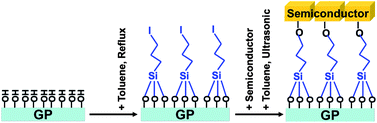 | ||
| Scheme 1 Process of assembling semiconductor monolayer on a glass plate (GP). | ||
Fig. 1 shows SEM images of TiO2, SrTiO3, ZnO and BaTaO2N particles deposited on GPs using carbosilane as a molecular linker. It can be seen that monolayers of particulate semiconductors are dispersed uniformly on the GP surface. No second layer of particles is observed, indicating that the molecular linker forms bonds selectively between the GP and oxide/oxynitride surfaces, and that the ultrasonic post-treatment is effective in washing away the physically absorbed particles from the immobilized particles to avoid a second layer. The morphology of the particles is regular in the case of TiO2 and BaTaO2N, and irregular in the case of SrTiO3 and ZnO. A monolayer can be prepared on a GP irrespective of the morphology, indicating that the binding strength of the molecular linker is sufficient to hold the semiconductor on the GP even with a small interfacial area. However, a monolayer composed of uniform particles (in the case of BaTaO2N) tends to exhibit a more organized and denser assembly with a higher GP coverage, consistent with trends reported in the literature.12–16
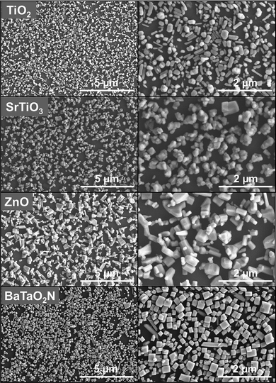 | ||
| Fig. 1 SEM images of TiO2, SrTiO3, ZnO and BaTaO2N monolayers deposited on GPs. | ||
Fig. 2 shows XRD patterns of monolayer particles deposited on a GP. For comparison, XRD patterns of the powder precursors are presented as well. It was found that the relative peak intensities for the crystalline facets of the monolayer on the GP were completely different from those for the randomly distributed powder precursors. The crystalline indices of the main peaks for the SrTiO3, ZnO and BaTaO2N samples were (110), (101) and (110), respectively, in the case of the powders, and (200), (100) and (200), respectively, in the case of the monolayers on GPs. For the TiO2 samples, the intensity of the main peak (110) for the powder precursors increased after the powders were assembled into monolayers on GPs. Table S1† shows the ratio of the peak intensities in each XRD pattern, calculated using the data in Fig. 2. As seen in Table S1†, the peaks associated with several crystal indices vanished after monolayer fabrication. According to Bragg's law, the intensity of a given reflection (h, k, l) is proportional to the number of h, k, l planes, and only the crystal planes parallel to the sample stage can be recorded by the detector. Here, the XRD pattern of the monolayer was recorded by holding the GP parallel to the sample stage of the XRD equipment, which means that each particle in the monolayer could be characterized and all crystal planes derived from detected diffraction lines were parallel to the GP substrate. On the basis of Fig. 1 and 2, and Table S1†, it is concluded that the following crystal planes can be assembled on a GP: the (110) and (220) planes of TiO2; the (100), (111), (200) and (110) planes of SrTiO3; the (002) and (100) planes of ZnO; the (100) and (200) planes of BaTaO2N. The change in the relative peak intensity in going from powder to monolayer can provide further clues as to the main crystal planes assembled on the GP. Let us take ZnO as an example. The I(002)![[thin space (1/6-em)]](https://www.rsc.org/images/entities/char_2009.gif) :I(100) ratio decreased fifteen-fold in going from a powder to a monolayer (Table S1†), which means that the (100) planes of ZnO are the most abundant crystal faces oriented in parallel to GP. Although crystal facets of ZnO appears to be varied in the SEM image (Fig. 1), we suppose that the linker binds more strongly with the facet of ZnO (100), resulting in the unique XRD pattern of the monolayer (Fig. 2).
:I(100) ratio decreased fifteen-fold in going from a powder to a monolayer (Table S1†), which means that the (100) planes of ZnO are the most abundant crystal faces oriented in parallel to GP. Although crystal facets of ZnO appears to be varied in the SEM image (Fig. 1), we suppose that the linker binds more strongly with the facet of ZnO (100), resulting in the unique XRD pattern of the monolayer (Fig. 2).
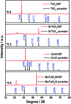 | ||
| Fig. 2 XRD patterns of TiO2, SrTiO3, ZnO and BaTaO2N powders and monolayers deposited on GPs. | ||
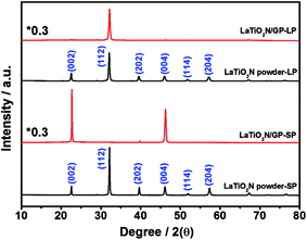
It is assumed that varying the morphology and/or particle size can change the selectivity for the types of exposed crystal facets favored during monolayer deposition on a GP. Here, we synthesized LaTiO2N semiconductors with large (L) and small (S) particle sizes (see ESI†) as precursors for assembling monolayers on GPs. SEM images of the LaTiO2N/GP monolayers are shown in Fig. 3. It can be seen that densely assembled monolayers were deposited on the GPs for both types of LaTiO2N particles. The large particles were around 1000 nm with a rectangular morphology, while the small particles were around 140 nm with a cubic morphology. XRD patterns of the LaTiO2N powders and monolayers are presented in Fig. 4. The relative peak intensities of the XRD patterns for large and small LaTiO2N particles were almost the same, while those of the assembled monolayers were completely different. For both powder precursors, the strongest peak for LaTiO2N crystallites was (112). The (112) peak almost disappeared in the case of the small-particle monolayer, while it was strengthened in the case of the large-particle monolayer. Table S2† presents the calculated values of the relative peak intensity of large and small LaTiO2N particles on the basis of the data in Fig. 4. As can be seen, from powder to monolayer, the value of the relative peak intensity I(004):I(112) decreased from 0.174 to 0.008 for the large particles and increased from 0.177 to 201 for the small particles. The difference in orientation between the large and small LaTiO2N particles was probably because of the difference in the surface area of the exposed crystal faces: the widest crystal face was (112) for the large particles and (002) for the small particles.
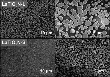 | ||
| Fig. 3 SEM images of LaTiO2N monolayers on GPs with large (L) and small (S) particles. | ||
 | ||
| Fig. 4 XRD patterns of LaTiO2N powder and monolayer with large (L) and small (S) particles. | ||
In the process of experiment, it can be seen from SEM that the particle morphology tends to have “redistribution” from powder to monolayer especially for BaTaO2N and LaTiO2N. The particles with irregular morphology have higher percentage in powder precursors than in monolayers. It was reported16 that the assembly of semiconductor particles involves a dynamic process in the present ultrasonic method, i.e., under ultrasonic conditions, the chemical bonds between the linker and the hydroxyl groups on the semiconductor break and reform continuously. Consequently, for the polycrystalline particles, those crystal faces with more hydroxyl groups are thought to bind more strongly to the GP. The number of reactive hydroxyl groups can be influenced by several factors, such as the crystal index, particle morphology and surface flatness. Taking flatness as an example, the size of the linker (IP-TMS) is less than 1 nm, which is much smaller than the particle size of the semiconductors tested in this paper. The presence of any tiny bulge on the surface of particle or GP inhibits the adequate connection between the linker and the bulk semiconductor. The ability to produce monolayers with highly regular facets has great potential for a variety of applications. Such monolayers can be used as seeds to grow single-crystal films, which can find application in, for example, the photoelectrochemical process for water splitting.
On the basis of the covalent reaction between a carbosilane molecular linker and surface functional groups on a substrate and oxides/oxynitrides, semiconductor monolayers were fabricated on GPs. The selective enhancement of the peak intensities in the XRD patterns of the monolayer samples indicates that specific crystal planes were organized and assembled uniformly on the GPs. The crystal planes bound to the substrate can be controlled by varying the morphology of the polycrystalline powder precursors. The proposed method of assembling specific crystal planes can be extended to other semiconductors using the general procedure established in this study.
Acknowledgements
This work was supported by the Development in a New Interdisciplinary Field Based on Nanotechnology and Materials Science program of the Ministry of Education, Culture, Sports, Science and Technology (MEXT), Japan, and by the Global COE Program (Chemistry Innovation through Cooperation of Science and Engineering) of the MEXT, Japan.Notes and references
- J. Aizenberg, D. A. Muller, J. L. Grazul and D. R. Hamann, Science, 2003, 299, 1205 CrossRef CAS.
- K. A. Perrine and A. V. Teplyakov, Chem. Soc. Rev., 2010, 39, 3256 RSC.
- N. Tian, Z. Zhou, S. Sun, Y. Ding and Z. Wang, Science, 2007, 316, 732 CrossRef CAS.
- H. Yang, C. Sun, S. Qiao, J. Zou, G. Liu, S. C. Smith, H. Cheng and G. Lu, Nature, 2008, 453, 638 CrossRef CAS.
- L. Kavan, M. Gratzel, S. E. Gilbert, C. Klemenz and H. J. Scheel, J. Am. Chem. Soc., 1996, 118, 6716 CrossRef CAS.
- B. D. Sosnowchik, H. C. Chiamori1, Y. Ding, J. Ha, Z. Wang and L. Lin, Nanotechnology, 2010, 21, 485601 CrossRef.
- D. Wang, H. Jiang, X. Zong, Q. Xu, Y. Ma, G. Li and C. Li, Chem.–Eur. J., 2011, 17, 1275 CrossRef CAS.
- G. Liu, J. C. Yu, G. Q. Lu and H.-M. Cheng, Chem. Commun., 2011, 47, 6763 RSC.
- (a) W. K. Burton and N. Cabrera, Discuss. Faraday Soc., 1949, 5, 33 RSC; (b) W. K. Burton and N. Cabrera, Discuss. Faraday Soc., 1949, 5, 40 RSC; (c) F. C. Frank, Discuss. Faraday Soc., 1949, 5, 48 RSC; (d) A. Halder, P. Kundu, B. Viswanath and N. Ravishankar, J. Mater. Chem., 2010, 20, 4763 RSC; (e) B. Viswanath, P. Kundu, A. Halder and N. Ravishankar, J. Phys. Chem. C, 2009, 113, 16866 CrossRef CAS.
- (a) M. Levy, R. M. Osgood, Jr, R. Liu, L. E. Cross, G. S. Cargill, III, A. Kumar and H. Bakhru, Appl. Phys. Lett., 1998, 73, 2293 Search PubMed; (b) R. M. Roth, D. Djukic, Y. S. Lee, R. M. Osgood, Jr, P. A. Lewis, S. Bakhru and H. Bakhru, Appl. Phys. Lett., 2007, 90, 112913 Search PubMed; (c) K. Petersen, Proc. IEEE, 1982, 70, 420 CrossRef CAS.
- (a) A. R. Tao, S. Habas and P. Yang, Small, 2008, 3, 310 CrossRef; (b) Y. Li, Q. Liu and W. Shen, Dalton Trans., 2011, 40, 5811 RSC.
- (a) N. Bowden, A. Terfort, J. Carbeck and G. M. Whitesides, Science, 1997, 276, 233 CrossRef CAS; (b) Q. Li, U. Jonas, X. S. Zhao and M. Kappl, Asia-Pac. J. Chem. Eng., 2008, 3, 255 Search PubMed; (c) I. D. Hosein, B. S. John, S. H. Lee, F. A. Escobedo and C. M. Liddell, J. Mater. Chem., 2009, 19, 344 RSC; (d) I. D. Hosein and C. M. Liddell, Langmuir, 2007, 23, 10479 CrossRef CAS; (e) B. R. Jackson, X. Liu, E. F. McCandlish and R. E. Riman, Langmuir, 2007, 23, 11399 Search PubMed; (f) Y. Wang and W. Zhou, J. Nanosci. Nanotechnol., 2010, 10, 1563 CrossRef CAS.
- X. Liu, E. F. McCandlish, L. E. McCandlish, K. Mikulka-Bolen, R. Ramesh, F. Cosandey, G. A. Rossetti and R. E. Riman, Jr, Langmuir, 2005, 21, 3207 CrossRef CAS.
- J. A. Lee, L. Meng, D. J. Norris, L. E. Scriven and M. Tsapatsis, Langmuir, 2006, 22, 5217 CrossRef CAS.
- (a) J. S. Lee, Y. Lee, E. L. Tae, Y. S. Park and K. B. Yoon, Science, 2003, 301, 818 CrossRef CAS; (b) K. Ha, Y. Lee, H. J. Lee and K. B. Yoon, Adv. Mater., 2000, 12, 1114 CrossRef CAS; (c) G. S. Lee, Y. Lee and K. B. Yoon, J. Am. Chem. Soc., 2001, 123, 9769 CrossRef CAS; (d) J. S. Park, G. S. Lee, Y. Lee, Y. S. Park and K. B. Yoon, J. Am. Chem. Soc., 2002, 124, 13366 CrossRef CAS; (e) K. Ha, J. S. Park, K. S. Oh, Y. Zhou, Y. S. Chun, Y. Lee and K. B. Yoon, Microporous Mesoporous Mater., 2004, 72, 91 CrossRef CAS; (f) K. B. Yoon, Acc. Chem. Res., 2007, 40, 29 CrossRef CAS.
- J. S. Lee, K. Ha, Y. Lee and K. B. Yoon, Adv. Mater., 2005, 17, 837 CrossRef CAS.
- (a) X. Chen, S. Shen, L. Guo and S. S. Mao, Chem. Rev., 2010, 110, 6503 CrossRef CAS; (b) A. Kudo and Y. Miseki, Chem. Soc. Rev., 2009, 38, 253 RSC; (c) K. Maeda and K. Domen, J. Phys. Chem. C, 2007, 111, 7851 CrossRef CAS.
Footnote |
| † Electronic supplementary information (ESI) available. See DOI: 10.1039/c1ce06128c |
| This journal is © The Royal Society of Chemistry 2012 |