DOI:
10.1039/C1CE05868A
(Paper)
CrystEngComm, 2012,
14, 278-285
Controllable synthesis of novel Cu2O micro/nano-crystals and their photoluminescence, photocatalytic and field emission properties
Received
11th July 2011
, Accepted 26th September 2011
First published on 26th October 2011
Abstract
Herein, two kinds of micro/nano-sized single-crystalline cuprous oxide (Cu2O) crystals with novel porous cubic or hierarchical rod-like morphologies were successfully synthesized via a facile ethanol-assisted double-solvothermal method. It was found that the addition of ethanol in precursor solution is critical for the formation of hierarchical rod-like structures (to be called nano-bamboo shoots in this paper). The detailed growth mechanism analyses indicated that the morphology transition from micro-porous cubes to quasi-one dimensional (1D) nano-bamboo shoots was due to the occurrence of branching growth as the reaction time increased. Besides, the photoluminescence (PL) measurement was introduced to evaluate the quality of crystalline and the results revealed that VCu and VO+ existed in both typical samples. The photocatalytic abilities of the as-prepared Cu2O crystals were investigated for the photodegradation of methyl orange (MO), and the results demonstrated that the nano-bamboo shoots had excellent photocatalytic performance due to its unique hierarchical structure with most exposed {110} facets. Moreover, the field emission properties of as-prepared two samples were measured for the first time. The results indicated that the micro-porous cubes samples which contained branching structures with sharp tips possessed better field emission performance with a lower turn-on field of 3.1 V μm−1, lower threshold field of 11 V μm−1 and larger field enhancement factor of 2365, implying its potential application for field emission display devices.
1. Introduction
Cuprous oxide (Cu2O) is a p-type semiconductor metal oxide with a direct band gap of about 2.17 eV. It has captured great attention due to its potential application in solar energy conversion,1 photocatalysis,2,3 sensors,4,5 and metal-insulator-metal resistive switching memory.6 It is widely known that the morphology, size, geometry and spatial orientation have great influence on the fundamental properties of semiconductor micro/nano-materials. Therefore, in the past several decades, great efforts have been devoted to controllable synthesis of various Cu2O architectures.7–9 So far Cu2O crystals with different shapes have been synthesized, such as cubes,10 octahedra,11dodecahedra,12 polyhedra,13nanowires,14nanocages,15 multipods,16 hierarchical,17 and hollow structures.18 Generally, the overall photocatalytic activity of a semiconductor is mainly decided by three factors: (1) The adsorption ability of photocatalysts, (2) photoabsorption ability in the available light energy region, (3) the separation and transporting rate of the photogenerated electrons and holes in catalysts.19 Porous structures with large surface area have prospective applications in photocatalysts, because the large surface area can provide more surface sites for adsorption of reactant molecules, which makes the adsorption process more efficient. Furthermore, metal oxide quasi-1D nanostructures such as nanowires, nanotubes, nanorods and nanobelts may further improve the photodegradation ability because the electrons and excitons can transport efficiently through the smallest dimension. Besides, 1D nanostructures are ideal candidates for achieving good field emission performance due to their high aspect ratio geometry and small tip radius of curvature,20 and they are also highly attractive building blocks for electronic devices.21,22 What is more, porous and quasi-1D structures were also reported to have great gas sensing properties.23,24 However, the anisotropic growth of Cu2O molecules to form 1D single crystalline nanostructure without using templates is challenging work due to the primitive isotropic cubic crystal structure of cuprous oxide.14
In this paper, we adopted a facile and low-cost hydrothermal approach to artificially manipulate the morphologies of Cu2O micro/nano-crystals. Micro-porous cubes and quasi-1D nano-bamboo shoots were successfully synthesized for the first time simply by adjusting the reaction times, which were expected to have great photodegradation activities and field emission properties. To the best of our knowledge, the field emission investigation of Cu2O crystals has never been reported. Furthermore, the growth process was discussed to clarify the morphology transition from micro-porous cubes to nano-bamboo shoots. Two primary factors, namely the volume ratio of ethanol to deionized water in precursor solution and the reaction time, were considered to have the most significant influence on the final shapes of crystals in our experiments. Photoluminescence (PL) spectra was measured and analyzed in detail to evaluate the crystalline quality of the two typical samples. Cu2O crystals have long been used as photocatalysts and the comparative photocatalytic activities of the two typical samples were examined by MO photodegradation. Much higher photodegradation ability was observed for the nano-bamboo shoots, which can be attributed to the exposure of {110} facets. Furthermore, field emission properties of these novel Cu2O micro/nano-structures were investigated. The results indicate that the micro-porous cubes consist of a large amount of branching structures with sharp tips and possess better performance, as expected.
2.
Experimental methods
2.1 Preparation of Cu2O micro/nano-crystals
All the products were synthesized under mixed solvothermal conditions. All chemical reagents used in this experiment were analytical grade and used without further purification. Ethanol and deionized water were mixed to form a double-solvent system in this work. The experimental procedure was as follows: given amount of ethanol was added to deionized water to form a typical volume ratio (defined as R) of 1/3 and the total volume of solvents was 100 mL. Subsequently, 0.5 g Cu(CH3COO)2·H2O powder and 1 mL pyrrole were dissolved in the above mixture solvents to form the precursor with pH value about 5. The solution was stirred for about half an hour, and then transferred into a 100 mL stainless-steel autoclave with a Teflon liner. A piece of silicon slice was placed on the bottom of the autoclave. The autoclave was sealed and maintained at 180 °C for different times. When the reaction times were 3 h and 10 h, respectively, two kinds of novel micro/nano-structures were synthesized: micro-porous cubes and nano-bamboo shoots. After naturally being cooled to room temperature (28 °C), the silicon slice was taken out and its surface was covered with the reddish-brown precipitate. It was rinsed with distilled water and ethanol several times and then dried at 60 °C for 1 h.
2.2 Photocatalytic experiments
The investigation of photocatalytic activities was performed at room temperature, and methyl orange (MO) aqueous solution was chosen as a pollutant. The procedure was as follows: Cu2O yielded by one experiment was dispersed into 100 mL MO solution (10 mg L−1). Before irradiation, the suspension was stirred in the dark for about 5 h to evaluate the adsorption ability. To minimize the heat effect, the reactor was fixed on a big glass container which was filled with flowing water, and the air conditioning was also used. Solution was irradiated by an 18 W daylight lamp (20 cm above the reactor) and the MO concentration was analyzed by UV-vis spectrophotometer (UNICO 2802) every hour during the total irradiation time of 4 h.
2.3 Characterization
The morphologies and structures of the as-grown products were characterized by field emission scanning electron microscopy (FESEM, JEOL-JSM-6700F) at an accelerating voltage of 20 kV, transmission electron microscopy (Jeol, JEM-2100) at an accelerating voltage of 200 kV and X-ray powder diffraction (XRD, D/MAX 2550V) with Cu-Kα radiation (λ = 1.54178 Å). The steady-state photoluminescence (PL) spectra were carried out by a Jobin-Yvon LabRAM HR 800 UV spectrometer with a 50 mW He–Cd laser as the excited light, which is operated at a wavelength of 325 nm (3.82 eV). The samples were at room temperature for all measurements. Field emission properties were measured by a simple diode configuration in a vacuum chamber under a pressure of 5 × 10⁻⁵ Pa at room temperature. The silicon substrate with micro/nano-material (as a cathode) was separated from a phosphor/indium tin oxide (ITO)/glass anode by two Teflon spacers with a thickness of 400 μm. The size of the measured emission area was about 5 mm × 5 mm.
3. Results and discussion
3.1 Structure characterization
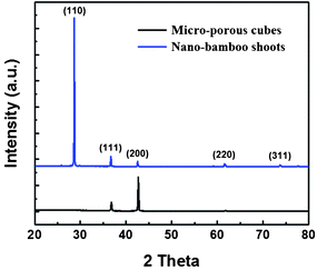
In these experiments, pyrrole was applied as a reductant. It was found that a lot of by-products, namely yellowish-brown hollow spherical poly(pyrrole) colloids, covered the sidewall of the autoclave, and the color of the solution after reaction was light green. Most of the precipitated products on the silicon substrates were Cu2O crystals, but some by-products were also contained in these samples. Fig. 1 plots the representative XRD patterns of the micro-porous cubes (black), and the nano-bamboo shoots structures (blue). All patterns can be indexed as the cubic phase of cuprous oxide (JCPDS card, No. 05-0667). No other characteristic peaks from impurities, such as CuO or Cu, were detected, revealing that the purity of the products was pretty high. It is well accepted that the facets with a lower growth rate will be exposed more on the crystal surface and consequently exhibit relatively stronger diffraction intensity in the corresponding XRD pattern.25 Thus according to the XRD data, for the micro-porous cubes, the (200) peak was higher than other peaks while almost no (110) peak was detected, implying more {200} facets are exposed on the crystal surface than the other facets. As regards to the nano-bamboo shoots, the overwhelmingly intense peak from the (110) diffraction planes suggests that the most exposed crystal surface was the {110} facets. The calculated value of intensity ratio between (110) and (200) is about 8.1 for this structure. The change of the peak position in these samples would reflect the growth mechanism of these crystal structures to some degree which will be discussed in the following passage.
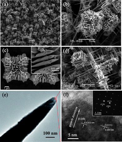
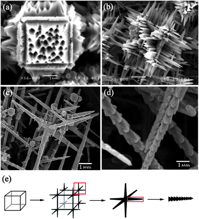
Fig. 2 presents the representative SEM and TEM images of a Cu2O sample prepared in the typical synthesis process when the reaction time was 3 h. Majority products in this sample are cubic-shaped porous particles with side lengths about 3–5 μm, so called micro-porous cubes as presented in Fig. 2(b)–(c). It is observed that there are holes with diameters ranging from tens of nanometres to over a hundred nanometres in body and the {100} surfaces of these cubes. The inset in Fig. 2(c) is the high magnification image of the substructure on the edge of a single porous cube, indicating that the twelve edges are composed of micro-plates with sharp edges which would further evolve into sharp-edged multi-branches. Furthermore, the surfaces of these substructures (micro-plates and multi-branches) are not smooth, and there are some nanoscale holes on the surfaces. Besides the cubic morphology discussed above, the other structure in this sample is micro/nano-scale multi-branches as shown in Fig. 2(d). These branches are perpendicular to each other and their lengths range from one micrometre to more than ten micrometres and all of them have sharp tips. The TEM image of a single nano-branch is displayed in Fig. 2(e). Fig. 2(f) presents the high-resolution TEM (HRTEM) image which corresponds to the rectangular area in Fig. 2(e). In this HRTEM image, the lattice spacing of 0.312 nm and 0.251 nm almost agree with the (110) and (111) planes of cubic-structured Cu2O respectively (the lattice spacing is 0.302 nm for (110) and 0.247 nm for (111) according to JCPDS file no. 05-0667). The inset in Fig. 2(f) illustrates the corresponding selected area electron diffraction (SAED) pattern. The combination of HRTEM and SAED indicate that the Cu2O branch is a single-crystalline and its preferential growth direction is [110]. This result confirms the XRD data that almost no (110) peak was detected because of the high growth rate along this direction.
 |
| | Fig. 2
Cu2O crystals synthesized for 3 h. (a) Low magnification SEM image. (b) Medium magnification SEM image of typical morphology (Cu2O micro-porous cubes). (c) High magnification SEM image of micro-porous cubes and the inset is the substructure on the edge of a single porous cube. (d) The other morphology (multi-branches) contained in this sample. (e) TEM image of a single nano-branch. (f) HRTEM image corresponds to the rectangular area in panel e. The inset displays the corresponding SAED pattern. | |
When the reaction time increased to 10 h and other experimental parameters remained typical, the morphology of the Cu2O crystal evolved into 1D submicron-rods with nanoscale hierarchical structures (so called nano-bamboo shoots) as shown in Fig. 3(a)–(c). The length of the Cu2O nano-bamboo shoots are about tens of micrometres and their diameter are typically 500–700 nm. Fig. 3(c) is the high magnification image of the nano-bamboo shoots. It is observed that the growth of burrs on the surface of micro-rods probably brought about the conical hierarchical structure along a micro-rod. Besides, it is noteworthy that the surfaces of these conical structures present to be porous as well. The TEM image of a single nano-bamboo shoot is shown in Fig. 3(d), where Fig. 3(e) is the higher magnification image of the rectangular area in Fig. 3(d) which presents one of the burrs grown on this morphology. In addition, the HRTEM image of the rectangular area in Fig. 3(e) is presented in Fig. 3(f) and inset is the corresponding SAED pattern. The lattice spacing of 0.415 nm would represent (100) planes of cubic-structured Cu2O while 0.309 nm almost agrees with (110) planes (according to JCPDS file no. 05-0667, their lattice spacing are 0.427 nm and 0.302 nm, respectively). The combination of these data reveals that the nano-bamboo shoots are single-crystal structures as well and the preferred growth orientation of burrs would be [100]. The TEM data can verify the XRD result that the intensity of (200) is much weaker than that of (110).
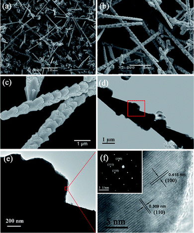 |
| | Fig. 3 (a) Low, (b) medium and (c) high magnification SEM images of Cu2O nano-bamboo shoots prepared for 10 h. (d) TEM image of a single nano-bamboo shoot. (e) High magnification TEM image of a single burr on the surface of nano-bamboo shoot as marked in the rectangular area of panel d. (f) HRTEM image corresponds to the rectangular area in panel e. The inset illustrates the corresponding SAED pattern. | |
3.2 Effect of the amount of ethanol
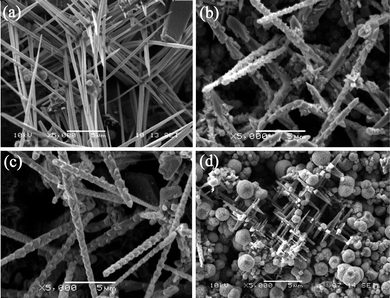
The addition of ethanol in the precursor was considered to be a key factor in the synthesis of these unique Cu2O micro/nano-crystal structures because no precipitates were collected in the absence of ethanol. Fig. 4(a)–(d) demonstrate the morphologies of the samples prepared with an increasing volume ratio of ethanol to deionized water (R). When R was 1/9, most of the products were Cu2O nanowires with diameter about 300 nm and their length was more than 10 μm, as shown in Fig. 4(a). These nanowires are not independent or separate from each other. However, the majority of cases are that every six Cu2O nanowires grow perpendicular to one another and all of them have almost smooth surfaces and sharp tips. Increasing R to 1/4, the morphology was developed into submicron-rods with small burrs grown on the surfaces. The diameter of these submicron-rods was approximately 600 nm and their length remained at about 10 μm. This may be due to the presence of ethanol which accelerated the reduction rate of Cu2+ and promoted the aggregating of Cu2O nanocrystals in the initial stage to minimize the total free energy of the system. With a further increase of R to 1/3, the typical nano-bamboo shoots were synthesized. However, as too much ethanol was mixed in the solvent, the amount of Cu2O crystals decreased greatly. Fig. 4(d) displays the sample prepared when R increased to 1/1. The majority of the products were spherical poly(pyrrole) colloids and only a little multi-branching structures were produced.
 |
| | Fig. 4
SEM images of Cu2O micro/nano-crystals synthesized with different volume ratio of ethanol to deionized water (R) for 10 h. (a) R = 1/9, (b) R = 1/4, (c) R = 1/3, (d) R = 1. | |
3.3 The time-dependent growth mechanism
It is proposed that the formation of Cu2O crystals with different morphologies may be related to the characteristics of the complex precursors synthesized in different reaction conditions.26 Because the only difference of synthesis between micro-porous cubes and nano-bamboo shoots is reaction time, a time-dependence growth mechanism is proposed in this paper. In order to clarify the crystal growth process of the two Cu2O crystals, keeping other typical parameters unchanged, products obtained from different reaction times (3 h, 5 h, 8 h, 10 h) are presented in Fig. 5(a)–(d). When the reaction time was 3 h, the Cu2O micro-porous cubes were formed as shown in Fig. 5(a). Further observation of these micro-porous cubes indicates that sharp branching growth took place perpendicular to the twelve edges of every cube. Prolonging reaction time to 5 h, the trend of branching growth became more obvious. As presented in Fig. 5(b), the branching growth rate on the apexes of cubic crystals was very high that the edges of cubes almost disappeared and every branch became longer and sharper. After reacting for 8 h, as shown in Fig. 5(c), most of products were multi-branch structures which formed by six branches grew across and perpendicular to each other. The branches grew ever longer and sharper, and meanwhile the surface of these branches became rough. With further increase of the reaction time to 10 h, the nano-bamboo shoots structure was formed (Fig. 5(d)).
 |
| | Fig. 5
SEM images of Cu2O micro/nano-crystals obtained with R = 1/3 for (a) 3 h, (b) 5 h, (c) 8 h, (d) 10 h. (e) The schematic representation of the transition from micro-porous cubes to nano-bamboo shoots. | |
Based upon our experimental results, the proposed schematic representation of the transition processes from micro-porous cubes to nano-bamboo shoots is depicted in Fig. 5(e). The growth procedure can be described as follows: Firstly, the micro-porous cubes are obtained which could be partially owing to the application of pyrrole as reductant and the addition of ethanol as solvent to promote the reduction rate. Previously reported that CuO/Cu2O composite mesoporous hollow microspheres were prepared by hydrothermal synthesis using Cu(CH3COO)2·H2O solution as precursor and macrospores were formed on the surface due to the aggregation, redistribution and reassembly of CuO nanoparticles containing amorphous or poorly crystallized phase.27 It is believed that the moderate reduction rate led to the phase transformation of CuO to high purity Cu2O crystals while their porous characteristics were preserved. In general, the crystal growth rate perpendicular to a plane is proportional to its surface energy, which results in the elimination of higher-energy surfaces while the lower-energy surfaces increase in area.25 The {100} planes have 100% saturated oxygen bonds while both {110} and {111} planes contain dangling Cu atoms, thus the {100} facets would have minimum surface energy.28,29 Hence, the cubic morphology with most exposed {100} planes was primarily formed. Owing to the continuous decrease of solute concentration, the growth would be under mass transport control which can generate a more concentrated zone on the apexes of crystals and less concentrated in the center of the face. Therefore, branching growth was favored29 and needle-like structure25 was preferentially formed. Besides, the concentration difference between the center and the apexes of crystals results in the faster growth rate on the apexes.30 With further increase of the reaction time, the growth rate on the apexes was very fast and the branching structure on the apexes of the cubes split into separate multi-branch structures with six branches grown across and perpendicular to each other. It is suggested that these branches would continually grow ever longer along their preferred orientation and then further split into separate 1D submicron-rods with hierarchical morphology. Because of the primitive isotropic cubic crystal structure of cuprous oxide, the anisotropic 1D growth of Cu2O crystals in aqueous condition was unstable and thus resulted in the emergence of burrs on the surface of the micro-rods. Hence, the formation of quasi-1D nano-bamboo shoots would be divided into two procedures: (1) 1D growth of primary submicron-rods, (2) growth of nanoscale burrs on the surface of the primary rods. As discussed above, the preferential growth direction of burrs is [100] and the facets with fast growth rate tend to shrink in size. Therefore, with the burrs increase in size, the {100} planes gradually disappear while the {110} facets appear. As a result, the most exposed crystal surfaces are no longer {100} facets, which is consistent with XRD data.
3.4 Photoluminescence properties
The PL measurement was introduced to understand the optical characteristics of the two typical Cu2O crystals. The excitation wavelength of 325 nm can reach the conduction band of Cu2O. Fig. 6(a) shows the measured PL emission spectra of the as-prepared micro-porous cubes and the nano-bamboo shoots structures at room temperature. The PL signals of the two samples are quite similar though the intensities of the peaks are relatively low for the nano-bamboo shoots. Generally, the peaks corresponding to the different electronic transitions can be classified into two main groups: the band-to-band transition (free exciton emissions) and the impurity transition (bound exciton emission from impurities).31 In order to determine the peak position of emissions, the Gaussian multipeak fitting was required. As Fig. 6(b)–(c) shows, a three-peak fit for the original PL signal was carried out to describe the PL profile of both samples. There are three peaks or shoulders at about 1.28 eV, 1.37 eV and 1.53 eV in both data. The red line in Fig. 6(b) and the blue line in Fig. 6(c) represent the sum of three peaks while the black line in both images represent the original PL signals, and they match each other satisfactorily. All three peaks attribute to the impurity transition and no apparent peak near the band edge appears, indicating that there are few free exciton emissions. The peaks at emitting energy around 1.28 eV and 1.37 eV are because of the emission from excitons bounded by copper vacancies (VCu, β-state) to VCu level (so-called β-luminescence),32 and the peak at 1.53 eV is because of the recombination of bound excitons at single charged oxygen vacancy (VO+).31 It is well known that the relative peak intensities depends on the relative vacancy concentration, these results imply that there are two main types of vacancies (VCu and VO+) in both samples and the concentration of VCu is a bit higher. W. C. Wang, et al.33 reported that VCu is the most stable defect and its formation is spontaneous during the growth of crystalline Cu2O in the vacuum-based environment. However, in a lower pH value environment, the formation energy of VO would decrease while the formation energy of VCu would rise. In our experiment, the pH value of precursor is about 5, which is an acid condition. This can explain why both VCu and VO+ were contained in the crystallographic structures of these samples. However, the less intense PL signal of nano-bamboo shoots may be because after reacting for a long time, the crystalline quality improved and thus fewer defects existed.
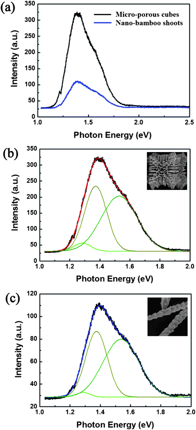 |
| | Fig. 6 (a) PL emission spectra of the two typical samples recorded at room temperature (about 28 °C). (b–c) The three-peak fit data for the PL emission spectra of (b) micro-porous cubes and (c) nano-bamboo shoots. | |
3.5 Photocatalytic activities
Methyl orange (MO) was used as a pollutant to evaluate the photocatalytic activities of the as-prepared two kinds of samples. Fig. 7(a), (b) display the absorption spectra of MO solution in the presence of Cu2O micro-porous cubes and Cu2O nano-bamboo shoots, respectively. It is clear that the photocatalytic ability of nano-bamboo shoots was much better than that of micro-porous cubes. Fig. 7(c) plots the degradation ability of these samples by monitoring the concentrations of MO solution at 463 nm with the maximum absorption, in which C/C0 stands for the concentration ratio after and before a certain reaction time. According to the data, after irradiation for 4 h, the remaining MO in solution is about 30% for micro-porous cubes and 7% for nano-bamboo shoots, indicating that the nano-bamboo shoots structure has more significant photocatalytic performance.
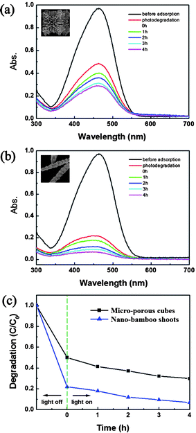 |
| | Fig. 7 (a–b) Absorption spectra of MO solution obtained at room temperature in the presence of (a) micro-porous cubes and (b) nano-bamboo shoots. (c) The extent of photodegradation of MO molecules (monitored at 463 nm) as a function of irradiation time for the two typical samples. | |
Previous studies found that the morphologies and the crystallographic structures have influence on the photocatalytic abilities of Cu2O crystals. For instance, Cu2O crystals with high-index facets would significantly enhance catalytic abilities for degradation of MO.34 The SEM image of nano-bamboo shoots after irradiation for 4 h in MO solution is presented in Fig. 8(a). Obviously, the burrs on the surface of the primary submicron-rods almost disappeared and their structure had high percentage of exposed {100} facets after irradiation. This results indicated that the high photocatalytic activity of the nano-bamboo shoots is mainly due to the burrs on the surface and their most exposed {110} facets. A unit cell of a Cu2O crystal is shown in Fig. 8(b), the blue spheres represent copper atoms and the red spheres indicate oxygen atoms. Cu2O has a cuprite crystal structure that has an oxygen atom is placed in the center and is surrounded by a tetrahedron of copper atoms in a unit cell. The surface atomic arrangements of {100} and {110} planes are presented in Fig. 8(c)–(d). The {100} planes have 100% saturated oxygen bonds and thus deduced a minimum energy state. However, the {110} planes contain positively charged Cu atoms with dangling bonds and have higher surface energy. What is more, the metallic character of the {110} plane structure is surface-like which may result in excellent catalytic activity related to the “Cu” dangling bonds of the {110} surfaces, so that {110} facets would interact more strongly with negatively charged MO molecules than {100} facets which appear to be electrically neutral.29 According to the above discussion, the most exposed facets are {200} facets for micro-porous cubes and {110} facets for nano-bamboo shoots. After photocatalytic reaction, the surface of nano-bamboo shoots became smooth and the most stable {100} facets remained. Hence, it is proposed that the exposure of {110} facets leads to much higher photocatalytic performance of nano-bamboo shoots in comparison with that of micro-porous cubes.
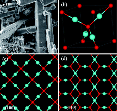 |
| | Fig. 8 (a) SEM image of nano-bamboo shoots after irradiation for 4 h in MO solution. (b) The unit cell of cuprite Cu2O structure. The blue spheres represent copper atoms and red spheres indicate oxygen atoms. (c–d) The atomic arrangements in the (c) (100) and (d) (110) planes of the Cu2O structure, respectively. | |
3.6 Field emission performances
Due to their unique morphologies, as mentioned above, the micro-porous cubes consisted of many branches with sharp tips on the surface and the nano-bamboo shoots with many burrs on the surface, are supposed to have good field emission properties. Field emission properties of the two typical samples were measured by the method mentioned in the experimental section. Considering the surface heights of these samples are not even, it is estimated that the maximum film thickness was 190 μm, so that the distance between electrodes was calculated to be 210 μm. The dependencies of the field emission current density on the applied electric field (J-E) and their corresponding Fowler-Nordheim (F–N) plots are presented in Fig. 9. It is clear that the Cu2O micro-porous cubes had better field emission properties with the lower turn-on field (defined as the field which was required to produce a current density of 0.1 μA cm−2) of about 3.1 V μm−1, and its threshold field (defined as the field where the current density reaches 1 mA cm−2) was around 11 V μm−1. For the nano-bamboo shoots, the turn-on field and threshold field were about 3.5 V μm−1 and 12.1 V μm−1, respectively. Generally, the field emission intensity primarily depends on the tip morphology and the density of these structures.35 Crystal morphology with higher density and sharper tips shows better field emission intensity. Thus the relatively better emission performance of micro-porous cubes may be attributed to the high aspect ratio of the branching structures contained in this sample, which have sharper tips than the burrs of nano-bamboo shoots. These sharp tips can effectively improve the field emission properties.
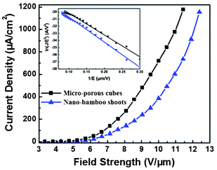 |
| | Fig. 9 The dependence of the field emission current density (J) on the applied electric field strength (E) of two typical samples. The inset shows the corresponding Fowler-Nordheim (F–N) plots. | |
The inset in Fig. 9 shows the corresponding F–N plots. The straight lines indicate that the emitting electrons mainly resulted from field emission. The dependence of emission current versus the applied voltage was analyzed by the Fowler-Nordheim equation:
| | 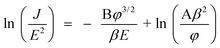 | (1) |
where A and B are constants, B = 6.83 × 10
9eV
−3/2Vm
−1,
β is the field enhancement factor, and
φ is the work function of the emitter material. According to
eqn (1), the field enhancement factor
β has an inverse ratio to the slope and can be described as follows:
| | 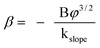 | (2) |
Assuming the work function φ of Cu2O was 4.84 eV,36 the field enhancement factor of Cu2O micro-porous cubes and nano-bamboo shoots were estimated to be 2365 and 2051, respectively. For both samples, the field enhancement factors are high enough for potential application in field emission display devices.
4. Conclusion
In summary, we described a double-solvent synthesis of single crystalline Cu2O micro-porous cubes and nano-bamboo shoots in the presence of ethanol under hydrothermal conditions. The growth mechanism was also discussed that the porous cubic structure was first formed in the ethanol–water system. Subsequently, branching growth and separation took place as the reaction progressed and finally developed into quasi-1D nano-bamboo shoots. PL properties revealed that both VCu and VO+ existed in two typical samples, and that the concentration of defects would decrease with an increase of reaction time. Both samples had good photocatalytic activities for the MO photodegradation while the performance of nano-bamboo shoots was better. Furthermore, the field emission properties of Cu2O structures were characterized for the first time. The results indicated that the field enhancement factors of the two typical samples were high enough for potential application in field emission display devices. Moreover, these novel porous and quasi-1D morphologies with large surface area are promising candidates for sensor applications in the future.
Acknowledgements
The authors acknowledge the financial support from the NSF of China (Grant No. 60976014, 60976004 and 11074075), the Key Basic Research Project of Scientific and Technology Committee of Shanghai (Grant No. 09DJ1400200) and the Program for Changjiang Scholars and Innovative Research Team in University (PCSIRT).
References and notes
- C. H. Kuo and M. H. Huang, Nano Today, 2010, 5, 106–116 CrossRef CAS.
- J. Y. Ho and M. H. Huang, J. Phys. Chem. C, 2009, 113, 14159–14164 CAS.
- H. Pang, F. Gao and Q. Y. Lu, CrystEngComm, 2010, 12, 406–412 RSC.
- L. Guan, H. Pang, J. Wang, Q. Lu, J. Yin and F. Gao, Chem. Commun., 2010, 46, 7022–7024 RSC.
- J. H. Zhong, G. R. Li, Z. L. Wang, Y. N. Ou and Y. X. Tong, Inorg. Chem., 2011, 50, 757–763 CrossRef CAS.
- A. Chen, S. Haddad, Y. C. Wu, T. N. Fang, S. Kaza and Z. Lan, Appl. Phys. Lett., 2008, 92, 013503 CrossRef.
- W. Q. Zhang, L. S, K. B. Tang and S. M. Dou, Eur. J. Inorg. Chem., 2010, 1103–1109 CrossRef CAS.
- X. Lan, J. Y. Zhang, H. Gao and T. M. Wang, CrystEngComm, 2011, 13, 633–636 RSC.
- Z. M. Yang, S. D. Sun, C. C. Kong, X. P. Song and B. J. Ding, J. Nanomater., 2010, 2010, 710584–710597 Search PubMed.
- H. Y. Zhao, Y. F. Wang and J. H. Zeng, Cryst. Growth Des., 2008, 8, 3731–3734 CAS.
- H. L. Xu, W. Z. Wang and W. Zhu, J. Phys. Chem. B, 2006, 110, 13829–13834 CrossRef CAS.
- X. Liang, L. Gao, S. Yang and J. Sun, Adv. Mater., 2009, 21, 2068–2071 CrossRef CAS.
- S. D. Sun, C. C. Kong, S. C. Yang, L. Q. Wang, X. P. Song, B. J. Ding and Z. M. Yang, CrystEngComm, 2011, 13, 2217–2221 RSC.
- Y. W. Tan, X. Y. Xue, Q. Peng, H. Zhao, T. H. Wang and Y. D. Li, Nano Lett., 2007, 7, 3723–3728 CrossRef CAS.
- C. Lu, L. Qi, J. Yang, X. Y. Wang, D. Y. Zhang, J. L. Xie and J. M. Ma, Adv. Mater., 2005, 17, 2562–2567 CrossRef CAS.
- Y. Chang and H. C. Zeng, Cryst. Growth Des., 2004, 4, 273–278 CAS.
- H. Zhang, Q. Zhu, Y. Zhang, Y. Wang, L. Zhao and B. Yu, Adv. Funct. Mater., 2007, 17, 2766–2771 CrossRef CAS.
- Y. Chang, J. J. Teo and H. C. Zeng, Langmuir, 2005, 21, 1074–1079 CrossRef CAS.
- Z. H. Ai, L. Z. Zhang, S. C. Lee and W. K. Ho, J. Phys. Chem. C, 2009, 113, 20896–20902 CAS.
- K. Yu, Y. S. Zhang, F. Xu, Q. Li and Z. Q. Zhu, Appl. Phys. Lett., 2006, 88, 153123 CrossRef.
- M. S. Arnold, P. Avouris, Z. W. Pan and Z. L. Wang, J. Phys. Chem. B, 2003, 107, 659–663 CrossRef CAS.
- D. P. Singh, N. R. Neti, A. S. K. Sinha and O. N. Srivastave, J. Phys. Chem. C, 2007, 111, 1638–1645 CAS.
- Q. Liu, W. M. Zhang, Z. M. Cui, B. Zhang, L. J. Wan and W. G. Song, Microporous Mesoporous Mater., 2007, 100, 233–240 CrossRef CAS.
- E. Comini, C. Baratto, G. Faglia, M. Ferroni, A. Vomiero and G. Sberveglieri, Prog. Mater. Sci., 2009, 54, 1–67 CrossRef CAS.
- Y. M. Sui, W. Y. Fu, H. B. Yang, Y. Zeng, Y. Y. Zhang, Q. Zhao, Y. G. Li, X. M. Zhou, Y. Leng, M. H. Li and G. T. Zou, Cryst. Growth Des., 2010, 10, 99–108 CAS.
- S. D. Sun, F. Y. Zhou, L. Q. Wang, X. P. Song and Z. M. Yang, Cryst. Growth Des., 2010, 10, 541–547 CAS.
- H. G. Yu, J. G. Yu, S. W. Liu and S. Mann, Chem. Mater., 2007, 19, 4327–4334 CrossRef CAS.
- Y. Zhang, B. Deng, T. R. Zhang, D. M. Gao and A. W. Xu, J. Phys. Chem. C, 2010, 114, 5073–5079 CAS.
- D. F. Zhang, H. Zhang, L. Guo, K. Zheng, X. D. Han and Z. Zhang, J. Mater. Chem., 2009, 19, 5220–5225 RSC.
- A. L. Daltin, A. Addad, P. Baudart and J. P. Chopart, CrystEngComm, 2011, 13, 3373–3377 RSC.
- H. S. Garranco, G. J. Diaz, A. E. Garcia, M. B. Garcia, M. G. Arellano, J. M. Juarez, G. R. Paredes and R. P. Sierra, J. Lumin., 2009, 129, 1483–1487 CrossRef.
- N. Harukawa, S. Murakami, S. Tamon, S. Ijuin, A. Ohmori, K. Abe and T. Shigenari, J. Lumin., 2000, 87, 1231–1233 CrossRef.
- W. C. Wang, D. X. Wu, Q. M. Zhang, L. C. Wang and M. Tao, J. Appl. Phys., 2010, 107, 123717 CrossRef.
- S. D. Sun, D. C. Deng, C. C. Kong, Y. Gao, S. C. Yang, X. P. Song, B. J. Ding and Z. M. Yang, CrystEngComm, 2011, 13, 5993 RSC.
- F. Xu, K. Yu, G. D. Li, Q. Li and Z. Q. Zhu, Nanotechnology, 2006, 17, 2855–2859 CrossRef CAS.
- W. Y. Yang and S. W. Rhee, Appl. Phys. Lett., 2007, 91, 232907 CrossRef.
|
| This journal is © The Royal Society of Chemistry 2012 |
Click here to see how this site uses Cookies. View our privacy policy here.