Crystal growth, characterization and thin disk laser operation of KLu1−xTmx(WO4)2/KLu(WO4)2 epitaxial layers
Martha
Segura
a,
Rosa Maria
Solé
*a,
Xavier
Mateos
a,
Joan J.
Carvajal
a,
Maria Cinta
Pujol
a,
Jaume
Massons
a,
Magdalena
Aguiló
a,
Sergei
Vatnik
b,
Ivan
Vedin
b,
Valentin
Petrov
c,
Uwe
Griebner
c and
Francesc
Díaz
a
aFísica i Cristal·lografía de Materials i Nanomaterials (FiCMA-FiCNA), Universitat Rovira i Virgili,(URV), Campus Sescelades, c/Marcel·lí Domingo s/n, 43007, Tarragona, Spain. E-mail: rosam.sole@urv.cat
bInstitute of Laser Physics, 13/3, av. Lavrentjeva, Novosibirsk, 630090, Russia
cMax-Born-Institute for Nonlinear Optics and Ultrafast Spectroscopy, 2A Max-Born-Street, D-12489, Berlin, Germany
First published on 24th October 2011
Abstract
Epitaxial samples of KLu1−xTmx(WO4)2/KLu(WO4)2 (x up to 0.15) have been obtained by the Liquid Phase Epitaxy (LPE) method. The lattice mismatch between the epitaxial layer and the substrate is small enough to allow the growth of good quality, well-oriented, single crystalline epilayers as evidenced by the 2θ scan of the (0k0) reflections and the rocking curve of the (040) reflection. Electron probe microanalysis shows an increase of 1021Tm3+ at cm−3 in a 2.5 μm interval at the substrate/layer interface. The main morphologies observed in the epilayers are steps and growth spirals. The laser operation around 2 μm, realized with epitaxial layers of 15 at% Tm doping and three different thicknesses, in a thin disk laser configuration with only two pump passes through the epitaxial layer, demonstrates maximum average output power as high as ∼1.4 W corresponding to a slope efficiency of 40%.
Introduction
Monoclinic KLu(WO4)2 (abbreviated as KLuW) is a highly anisotropic biaxial crystal that crystallizes in the C2/c space group with cell parameters: a = 10.576(7) Å, b = 10.214(7) Å, c = 7.487(2) Å, β = 130.68(4)° and Z = 4.1The large absorption and emission cross-sections of trivalent lanthanide ions, partially due to the strong anisotropy of KLuW, together with the relatively large ion separation, allow large concentrations of lanthanide active ions without significant fluorescence quenching which makes this crystal host attractive for solid state lasers.2
Among all the lanthanide active ions, Tm3+ is very interesting for laser emission at wavelengths near 2 μm which have applications in the field of medicine, mainly due to the strong optical absorption by water, and remote sensing (LIDAR) of CO2 and water in the atmosphere, as well as for pumping Optical Parametric Oscillators (OPOs) for conversion in the mid-IR.3 Recently, continuous-wave (CW) laser operation of bulk Tm:KLuW has been demonstrated with tunability extending from 1800 to 1987 nm, a maximum output power of 4 W and a slope efficiency of 69%.4 Furthermore, passive mode-locking of such a thulium bulk laser generating ∼10 ps pulses near 2 μm with an average power as high as 240 mW at a repetition rate of 126 MHz has also been achieved.5
Lasers based on thin films in thin disk configuration have several advantages such as high beam quality and optical efficiency, and it is possible to obtain high power with low thermal lensing because heat removal efficiency from thin layers is improved in comparison to bulk crystals.6 Increasing the doping level and simultaneously reducing the crystal thickness are essential for improving the thermal management through the larger surface to volume ratio and for a reduction in the number of pump passes to take advantage of the benefits of the doped monoclinic double tungstates. Such thulium doped active laser elements for thin disk configurations can be obtained by liquid phase epitaxy (LPE) growth of monoclinic Tm:KLuW layers on KLuW. CW laser operation of such a KLu0.945Tm0.055(WO4)2/KLu(WO4)2 (010) epitaxial layer was first demonstrated in an astigmatically compensated X-type cavity, yielding a slope efficiency of 64%.7 More recently, a highly doped KLu0.845Tm0.155(WO4)2/KLu(WO4)2 (010) epitaxial structure was employed for laser operation in the thin-disk configuration using an 80 μm thick epilayer. The maximum output power in the CW regime reached 550 mW with an efficiency of 11.2%.8,9 Furthermore, Tm3+:KY1−xGdxLuy(WO4)2/KY(WO4)2 and Yb3+:KGd1−xLux(WO4)2/KY(WO4)2 epitaxies have been grown by LPE to develop channel waveguide lasers for integrated optics applications.10,11
Laser efficiency depends on the quality of the crystal and the substrate–epilayer interface, as well as the thickness and the level of doping. Therefore, a study on how the doping level and the growth conditions affect the quality and thickness of the epilayer is important in order to optimize the laser performance of Tm:KLuW epitaxial layers. We present here studies of the growth velocity, the layer quality, the possible mechanisms of epitaxial growth and the presence of structural defects as functions of various growth parameters.
We also present laser operation around 2 μm, for better comparison initially realized in the quasi-CW (QCW) mode of operation, with three KLu0.845Tm0.155(WO4)2/KLu(WO4)2 epilayers of the same doping level but different thickness, achieving output power and efficiency well above those previously reported in ref. 9.
Experimental details
Substrate crystal growth
KLuW has a polymorphic phase transition at 1298 K while the phase of interest for laser emission is the monoclinic low temperature phase. Therefore, KLuW crystals were grown from high temperature solutions.12 The solvent used was K2W2O7 because of the absence of foreign ions thereby minimizing contamination and its low melting temperature.13 For single crystal growth we employed the Top Seeded Solution Growth-Slow Cooling (TSSG-SC) method.The crystal growth experiments were carried out in a cylindrical vertical furnace as described elsewhere.14 The starting materials were K2CO3, Lu2O3 and WO3 with purities of 99%, 99.99% and 99.5%, respectively. The solution, with a weight of about 200 g, was prepared in a 125 cm3 cylindrical platinum crucible. Its composition, to grow substrates, was 12 mol% KLuW–88 mol% K2W2O7 according to the solubility curve obtained previously.13 The axial thermal gradient in the solution was around 1 K cm−1, with the surface of the solution colder than the bottom. The orientation of the seed was along the crystallographic b direction because previous results indicate that this orientation is the best in order to obtain good quality crystals.15 After measuring the saturation temperature of the solution,15 the seed was maintained in contact with the surface of the solution, while the furnace was cooled down slowly at a rate of 0.1–0.2 K h−1 for about 15–20 K in order to supersaturate the solution for crystal growth. During the entire growth process, the crystal was rotated at a rate of 40 rpm. When the crystal was sufficiently large in size, it was removed slowly from the solution and maintained slightly above the solution surface while the furnace was further cooled down at a rate of 25 K h−1.
The substrates for LPE growth were obtained by cutting, with a diamond saw, the bulk crystals in slices perpendicular to the crystallographic b direction. The dimensions of the first type of plates, to be used as substrates with the crystallographic c direction perpendicular to the surface of the solution (hereafter c oriented substrates), were about 5–6 mm × 2 mm × 9–12 mm along the a*, b and c crystallographic directions, respectively. A second type of substrates was used, with a* perpendicular to the surface of the solution (hereafter a* oriented substrates); their typical dimensions were 12–15 mm × 2 mm × 6–7 mm, along the a*, b and c crystallographic directions, respectively. After cutting, the substrates were polished with diamond powder to achieve a rms roughness lower than 50 nm.
Liquid phase epitaxial growth
The LPE growth runs were carried out in a special furnace built to have a nearly homogeneous temperature in the whole solution.14The starting materials used to prepare the solution were the same as used for the crystal growth of substrates and Tm2O3 (99.9% purity) substituting Lu2O3 was added for doping purposes. The solutions were prepared in 30 cm3platinum cylindrical crucibles and weighed about 70 g. The solution composition was 7 mol% Tm:KLuW–93 mol% K2W2O7 with different levels of substitution of Lu by Tm.
Once the solution was homogenized, accurate measurements of the saturation temperature and the kinetics of the growth/dissolution processes were carried out using a KLuW seed.13 These measurements were later used to select the temperature and growth time of the epitaxial layers.16Table 1 summarizes the experiments of epitaxial growth of Tm:KLuW over KLuW substrates with a* or c orientation for Tm2O3 substitution of Lu2O3 in the solution ranging from 5 to 15 mol%.
| Exp. | at% Tm | Substrate orientation | Growth time/h | K Tm | Crystal composition | Surface morphologies |
|---|---|---|---|---|---|---|
| 1 | 5 | c | 4 | 1.10 ± 0.06 | KLu0.945Tm0.055(WO4)2 | Flat surface |
| 2 | 5 | c | 1, 2.5, 7, 20, 22, 26 | Flat surface with growth steps | ||
| 3 | 7.5 | c | 4 | 1.15 ± 0.02 | KLu0.913Tm0.087(WO4)2 | Flat surface, some spirals and hillocks |
| 4 | 7.5 | a* | 4 | Flat surface | ||
| 5 | 10 | c | 4 | 1.03 ± 0.02 | KLu0.897Tm0.103(WO4)2 | Spirals and steps |
| 6 | 10 | c | 5 | Flat surface, some spirals | ||
| 7 | 10 | a* | 4 | Pyramids, inclusions and steps | ||
| 8 | 15 | c | 5 | 1.04 ± 0.02 | KLu0.845Tm0.155(WO4)2 | Flat surface |
| 9 | 15 | c | 17 | Flat surface | ||
| 10 | 15 | c | 21 | Flat surface, some steps and spirals | ||
| 11 | 15 | c | 24 | Flat surface, cracks |
The substrates were cleaned, as described in ref. 16, before introducing them into the furnace. They were introduced slowly into the furnace in order to avoid thermal stresses and maintained for 1 h above the solution surface to reach thermal equilibrium with the solution. After that, the substrates were dipped in the solution at a temperature of 1 K above the saturation temperature and maintained at this temperature for 5 minutes, in order to slightly dissolve their surface. The solution temperature was then decreased down to 6 K below the saturation temperature, which represents a supersaturation of 5.3%.6 During the entire epitaxial growth process, the substrate was rotated at 40 rpm. In experiment 2 in Table 1, the substrate was introduced several millimetres into the solution and was then pulled out in discrete steps, at known time intervals, to study the effect of the growth time on the thickness and quality of the epitaxial layer.
The level of substitution of Lu3+ by Tm3+ in the epilayers was measured by electron probe microanalysis with wavelength dispersive spectroscopy (EPMA-WDS) using a Cameca SX 50 equipment. Corrections for dead time, background and matrix effects were carried out using the Pouchou and Pichoir (PAP) procedure.17 The actual composition of the epilayers for different levels of Lu3+ substituted by Tm3+ in the solution is also shown in Table 1, together with the calculated distribution coefficient of Tm3+ in these layers.
The surface of the epitaxial layers was inspected with a SENSOFAR PLμ 2300 confocal microscope in order to evaluate the sample roughness and the height and width of the steps in different parts of the layer. The epitaxial thickness was measured also by the confocal microscope. In some experiments, the layer thickness was also measured by EPMA to verify the suitability of the microscope method used.
X-Ray diffraction
To complete the data we previously presented in ref. 18, we have calculated the unit cell parameters of KLu0.845Tm0.155(WO4)2. To obtain small single crystals for X-ray powder diffraction measurements, we used a solution with composition 7 mol% Tm:KLuW–93 mol% K2W2O7 and 15 mol% of Tm2O3 substituting Lu2O3. After the homogenization of the solution, a platinum disk, 12 mm in diameter, rotating at 40 rpm, was dipped into the solution. Then, the solution temperature was decreased in steps of 10 K every 30 minutes until crystals were nucleated on the disk. After that, the solution temperature was decreased at a rate of 0.5–1 K h−1 for 10 K to grow the crystals. After removing the crystals from the solution and cleaning them, they were powdered for X-ray diffraction measurements.The X-ray powder diffraction patterns were obtained using a Siemens D-5000 powder diffractometer, with Bragg-Brentano parafocusing geometry and vertical θ–θ goniometer. The measurements were carried out at 2θ = 10–70°, a step size of 0.02° and a step time of 16 s. The unit cell parameters were refined with the Fullprof program19 using all the peaks in the range 2θ = 10–70°. From these results, we calculated the lattice mismatch, at room temperature, between Tm:KLuW and KLuW for different Tm contents.
In order to evaluate the crystallinity of the epitaxial layer and the substrate, X-ray diffraction measurements on the epitaxial layer and the substrate of a KLu0.845Tm0.155(WO4)2/KLu(WO4)2 sample were carried out, using a Bruker-AXS D8-Discover diffractometer equipped with parallel incident beam (Göbel mirror), a vertical goniometer equipped with a collimator for the X-ray beam of 500 μm and a GADDS (General Area Diffraction System) detector of 30 × 30 cm with a 1024 × 1024 pixel CCD sensor. Cu radiation was obtained from a copper X-ray tube operating at 40 kV and 5 mA. First, a 2θ scan was recorded on the substrate and after that on the epilayer in order to check their orientations. Data were recorded in two different steps with the area detector by performing an ω-scan with a frame width of 15° in the θ range 5–35° and with an integration time of 60 s per frame. The 2θ patterns of the substrate and the film reveal only the (0k0) reflections, which indicate that the substrate and the film surfaces are perpendicular to the crystallographic b direction. After that, an XRD ω-scan (rocking curve) of the (040) reflection of the epitaxial layer and of the substrate were carried out separately, in order to determine their crystalline quality. This was necessary because the film was too thick to record the rocking curves of both the epitaxial layer and the substrate simultaneously. The measurements were performed with the same diffractometer with a width of 4°, a step size of 0.02° and an integration time of 5 s per frame.
Thin disk laser samples
Due to the anisotropy of KLuW, optical absorption is strongly dependent on the light polarization. The optical ellipsoid in such biaxial crystals is defined by the three orthogonal principal axes Np, Nm and Ng with associated refractive index values np < nm < ng.1 In bulk Tm-doped KLuW, the maximum absorption cross-section of the electric dipole transition 3H6 → 3H4 for E‖Nm amounts to σabs = 5.95 × 10⁻²⁰ cm2 (FWHM = 4 nm) at 802 nm.3 To confirm the final thickness of the epilayers, after the cut and polishing process, this thickness was calculated using the value of the transmittance of the samples for thin disk experiments for light polarized along Nm at the maximum absorption.The epitaxy faces were high-reflection (HR) coated for laser (1800–2000 nm) and pump (802 nm) wavelengths and bonded to an indium plated copper heat sink with a thermo-conductive epoxy. The heat sink was cooled with a thermoelectric element to 20 °C. The substrate faces were anti-reflection (AR) coated for both laser and pump wavelengths. The pump source was an AlGaAs diode laser emitting at 805 nm with 20 W of maximum power and the pump spot onto the sample was 780 μm in diameter. A linear cavity was used with the epitaxy coated surface as an end mirror and an output coupler with radius of curvature Roc = −40 mm and transmission (Toc) of 2.8% in the 1800–2000 nm range.
Experimental results and discussion
Substrate crystal growth
The single crystals of KLuW grown by the TSSG method were colorless, transparent and free from inclusions and cracks. Fig. 1a shows a typical KLuW single crystal before being cut for substrates and in Fig. 1b there is a scheme showing the indices of the faces. As seen in the figure, the crystal habit is formed primarily by the {110}, {010} and {![[1 with combining macron]](https://www.rsc.org/images/entities/char_0031_0304.gif) 11} faces. Previous studies indicated that the growth on the (010) face has the highest velocity and also the best quality,10 which concurs with the poor development of this face in the bulk crystals and also with its F-face nature (large interplanar distance).1 According to the Hartman–Perdok theory, a layer by layer crystal growth mechanism on this face is expected. Furthermore, the (010) plane is a principal optical plane which permits the propagation of light perpendicular to it, with polarization E‖Nm for which this material presents the maximum absorption and emission cross-sections.
11} faces. Previous studies indicated that the growth on the (010) face has the highest velocity and also the best quality,10 which concurs with the poor development of this face in the bulk crystals and also with its F-face nature (large interplanar distance).1 According to the Hartman–Perdok theory, a layer by layer crystal growth mechanism on this face is expected. Furthermore, the (010) plane is a principal optical plane which permits the propagation of light perpendicular to it, with polarization E‖Nm for which this material presents the maximum absorption and emission cross-sections.
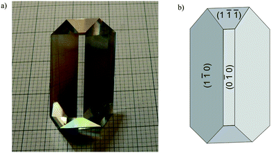 | ||
| Fig. 1 (a) As-grown KLuW bulk single crystal for substrate slicing (the small squares are 1 × 1 mm2) and (b) crystal scheme showing the indices of the faces. | ||
Liquid phase epitaxial growth
As already mentioned, the LPE experiments performed on cut and polished KLuW plates are summarized in Table 1. In all experiments, a superficial dissolution of the substrate took place by maintaining the solution temperature at 1 K above the saturation temperature for 5 min.The Tm3+ substitution of Lu3+ in the solution for LPE growth varied from 5 at% to 15 at%. No significant differences in the surface morphologies were observed for the two different substrate orientations, c and a* perpendicular to the surface of the solution (see Table 1), which were used. The distribution coefficient of Tm3+ in these crystals, included in Table 1, is calculated as: KTm = {[Tm]/([Tm] + [Lu])}crystal/{[Tm]/([Tm] + [Lu])}solution. The error in the Tm3+ concentration measurements is 5% for the epitaxial layers with lower Tm3+ concentration (5% Tm3+ substituting Lu3+ in the solution) and 2% for the other samples, while the error in the resulting distribution coefficient of Tm3+ is in the order of 10−2 as can be seen in Table 1. Also, the distribution coefficients are only slightly >1 and get closer to 1 for higher Tm3+ concentrations. The homogeneity of the epitaxial layer, studied by EPMA-WDS, was assessed by measuring the crystal composition in a direction perpendicular to the substrate/layer interface, from the outer part of the layer to the interface. As can be seen in Fig. 2, the epitaxial layer is homogeneous within the measurement error and the Tm3+ concentration change in the substrate/layer interface is on the order of 1021 at cm−3.
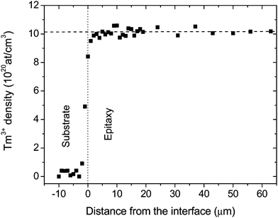 | ||
| Fig. 2 Tm-density distribution for the (010) face of the KLu0.845Tm0.155(WO4)2/KLu(WO4)2 epitaxial sample. | ||
The epitaxial layers were generally smooth, although when their thickness increases, morphologies such as growth spirals and steps were increasingly observed. When the growth rate was fast enough and the lattice mismatch was larger than 0.11, additional growth defects such as growth pyramids and solution inclusions were observed. As an example, Fig. 3a shows a photograph recorded on a confocal microscope of the interaction of two growth spirals of opposite sign obtained in the epitaxial layer grown in experiment 5 (Table 1). A similar growth morphology was also observed and studied in ref. 13 for the epitaxial growth of Yb:KLuW/KLuW.
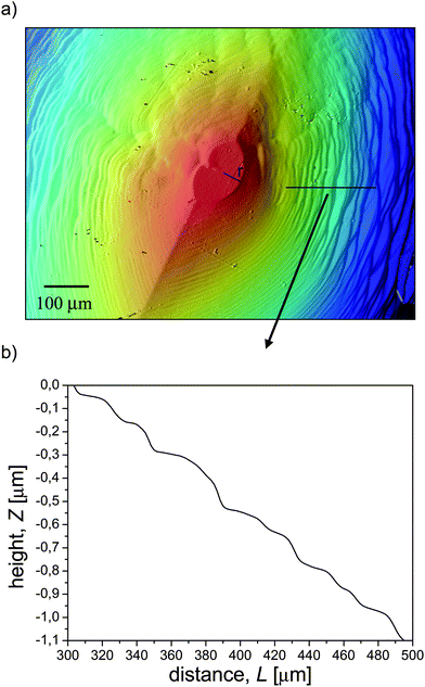 | ||
| Fig. 3 (a) Photograph of the interaction of two growth spirals of opposite sign observed in the KLu0.897Tm0.103(WO4)2/KLu(WO4)2 epitaxial layer obtained in experiment 5 (Table 1) and (b) profile of the growth steps at a distance from the center between 3 and 6 times the characteristic radius (r) of the central hillock. | ||
The width and height of the steps located around the central hillock were measured with the same microscope. It is observed that near the center, the steps have a height and width lower than their values at larger distances. At distances 3 to 6 times the characteristic radius (r) of the central hillock, typical steps of 10–15 μm high and 15–20 μm wide were observed (see Fig. 3). As in the case of Yb-doped epitaxial layers, no polygonalization of the micromorphologies has been observed, indicating a predominant role of the diffusion effects in the crystal growth rather than structural effects.13
Fig. 4a and b show the region where two growth spiral fronts collide. The collision region between the two spirals is clearly observed in the figure by a change in the direction of the steps. A profile of this region is shown in Fig. 4c. It can be seen that when two spirals collide, a depression is created and the height and width of the steps at both sides of the depression sometimes are slightly different, as in this example.
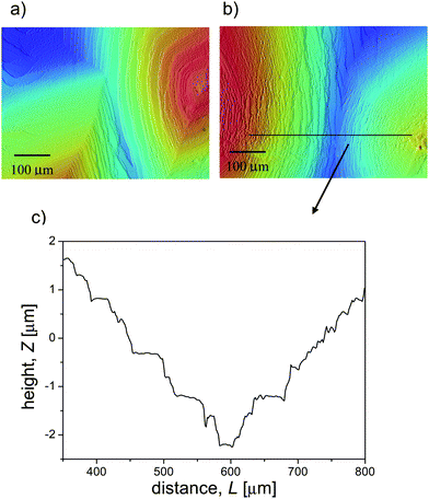 | ||
| Fig. 4 (a and b) Collision zone of two growth spiral fronts in the KLu0.897Tm0.103(WO4)2/KLu(WO4)2 epitaxial layer obtained in experiment 5 (Table 1), and (c) profile of the growth steps on both sides of the collision zone of the two spirals. | ||
Another defect that was observed when the Lu3+ substitution by Tm3+ in the epilayer was at least 10 mol% ((010) layer/substrate lattice mismatch larger than 0.11) is the presence of periodic inclusions.9 As an example, Fig. 5 shows a photograph (top view) of the periodic inclusions observed on epilayers grown on (010) faces for lattice mismatches larger than 0.11 and fast growth rates.
 | ||
| Fig. 5 Periodic inclusions observed in epilayers for high growth rates when the layer/substrate lattice mismatch exceeds 0.11. | ||
In experiment 2 (Table 1), as already mentioned, the effect of the growth time on the layer thickness was studied by keeping all the other growth conditions constant. For this study, a KLuW substrate was dipped several millimetres into the solution and after that it was pulled at known time intervals. Fig. 6 shows the variation of layer thickness with time of growth. As can be observed, there is a linear dependence of the epitaxial thickness on the growth time, at least up to 26 hours of growth, with a growth rate of 14.3 μm h−1. These results differ from the previously observed behavior in the epitaxial growth of Yb-doped KLuW layers, for which the growth velocity dropped with time, e.g. down to 7.1 μm h−1 after 22 h.13
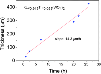 | ||
| Fig. 6 Layer thickness as a function of time of growth (experiment 2, Table 1). | ||
In order to optimize the pumping absorption versus the layer thickness for laser experiments, we grew several KLu0.845Tm0.155(WO4)2epitaxies in experiments 8 to 11 in Table 1.
X-Ray diffraction
The unit cell parameters of Tm:KLuW, for different Tm concentrations, are shown in Table 2. Using these data and the unit cell parameters of KLuW, the lattice mismatches between the substrate and the epitaxial layer were calculated. The expression used to calculate the lattice mismatch was f(hkl) = (S(hkl),(layer) − S(hkl),(subs))/S(hkl),(subs) where S(hkl),(layer) and S(hkl),(subs) are the areas obtained from the periodicity vectors (hkl) of the layer and the substrate, respectively. The results obtained are also presented in Table 2.| Epitaxial layer | a/Å | b/Å | c/Å | β/° | f{010} | f{100} | f{hkl} ⊥ c |
|---|---|---|---|---|---|---|---|
| KLu0.945Tm0.055(WO4)2 | 10.5934 | 10.2409 | 7.4994 | 130.745 | 0.0859 | 0.0873 | 0.0663 |
| KLu0.913Tm0.087(WO4)2 | 10.5937 | 10.2432 | 7.5001 | 130.744 | 0.0996 | 0.1191 | 0.0692 |
| KLu0.897Tm0.103(WO4)2 | 10.5941 | 10.2456 | 7.5006 | 130.740 | 0.1161 | 0.1492 | 0.0804 |
| KLu0.845Tm0.155(WO4)2 | 10.5950 | 10.2476 | 7.5018 | 130.744 | 0.1346 | 0.1848 | 0.1001 |
For all doping levels, the positive lattice mismatch indicates a compressive strain between the layer and the substrate, the epilayer being compressed. In ytterbium doped epitaxies the lattice mismatch tendency was f(100) > f(010) > f(hkl) ⊥ c. For thulium doping, as can be concluded from Table 2, the same behavior is observed.
From the 2θ scan of the substrate and the epitaxial layer of a KLu0.845Tm0.155(WO4)2/KLu(WO4)2 sample, showing only the (0k0) reflections (Fig. 7), one can conclude that the orientation of the film and the substrate is perpendicular to the b crystallographic direction and that both are single-crystalline. From the rocking curves of the (040) reflection in the epitaxial layer and the substrate of the same sample (inset of Fig. 7), one can see that there are no significant changes in the position of the peaks and the measurements of the FWHM intensity of the (0k0) reflections show similar values for the epitaxial layer and the substrate.
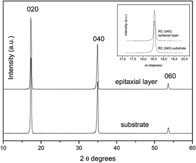 | ||
| Fig. 7 2θ scan of the (0k0) reflections in the epitaxial layer and the substrate of a KLu0.845Tm0.155(WO4)2/KLu(WO4)2 sample. Inset: rocking curve of the (040) reflection from the epitaxial layer and the substrate of the same sample. | ||
Laser experiments
The samples for laser experiments were 15 at% Tm doped with actual composition KLu0.845Tm0.155(WO4)2/KLu(WO4)2 and concentration of [Tm3+] = 1.01 × 10²¹ at cm−3 (calculated using an unit cell volume of 613.3 Å3). The final thicknesses of the three epilayers were 168, 253, and 476 μm, respectively, with an error of 2% (see Fig. 8) and the thickness of substrates was 2 mm. The as-grown epitaxy and the composite after polishing, coating and mounting in the copper holder for laser experiments are shown in Fig. 9.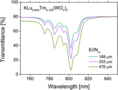 | ||
| Fig. 8 Polarized transmittance of the epitaxial samples in the 750–850 pump wavelength range, with estimation of the final thicknesses at room temperature. | ||
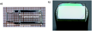 | ||
| Fig. 9 (a) The as grown Tm:KLuW/KLuW epitaxy (the squares are 1 × 1 mm2) and (b) the same sample after cutting, polishing, coating and mounting on the heat sink for laser experiments. | ||
The output power dependence is shown in Fig. 10 for all the samples in the QCW regime. The slope efficiencies, with respect to the absorbed power in double pass pumping, were in the 40–46% range and the maximum average output power amounted to ∼1.4 W, with the 476 μm thick epitaxial sample. These values are 3–4 times higher than those reported in ref. 8 under the same conditions. Thicker layers with increasing absorption seem to be more promising for scaling to higher output powers.
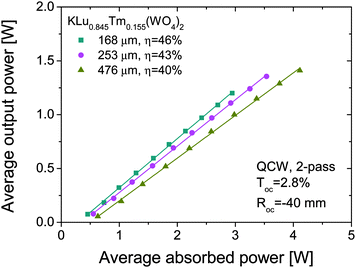 | ||
| Fig. 10 Output power of the epitaxial Tm:KLuW laser in the QCW regime with 18% duty cycle and double pass (through the epitaxial layer) pumping. | ||
As can be seen in Fig. 10, the maximum output power increases from 1.20 to 1.35 and 1.41 W, for 168, 253 and 476 μm thickness, respectively. However, this is a conclusion based on the fixed double pass pump configuration, Tm-concentration and other cavity parameters. In fact, even at the reduced thermal requirements defined by the QCW regime, the thinner samples indicate a trend of increasing efficiency presumably related to the mentioned aspect ratio.
The optimum length of the cavity was 15.5 mm in all cases. The laser emission spectra were centered at 1917, 1921 and 1947 nm for the 168, 253 and 476 μm thick epitaxial samples, respectively. The longer oscillation wavelengths for increasing epilayer thickness are a consequence of the increasing reabsorption. The threshold varies with layer thickness from 0.455 to 0.632 W and the estimated pump absorption of the epilayers under lasing conditions is 68%, 83% and 95%, respectively, showing good agreement with the low-signal transmission measurements.
Conclusions
High quality epitaxial layers of KLu1−xTmx(WO4)2 over (010) KLu(WO4)2 substrates have been obtained by the LPE method, with up to 15 at% of Lu3+ substituted by Tm3+ in the solution. EPMA measurements show a Tm3+ distribution coefficient very close to unity. From the results of EPMA, we also conclude that the epilayer is homogeneous within the measurement error. The lattice mismatch between the epitaxy and the substrate, with up to 15 at% of Lu3+ substituted by Tm3+, is less than 0.14 in the {010} plane, which makes it possible to obtain a layer/substrate interface free from macroscopic defects. The epitaxial layer is single-crystalline, as evidenced by the 2θ scan which reveals only the (0k0) peaks. The main morphologies observed in the grown layers are steps and growth spirals, although some pyramids and periodic inclusions have also been observed for fast growth rates and high levels of substitution.We have shown preliminary results on thin disk laser operation using 15 at% Tm doping and epitaxial layer thickness of 168, 253 and 476 μm. Optimum laser performance was characterized by a maximum output power of ∼1.4 W in the QCW regime corresponding to 40% slope efficiency, achieved with the 476 μm thick epitaxial sample in a two pass only pump configuration. Future work will focus on power scaling and further improvement of the laser efficiency by optimization of the doping level, variation of the output couplers and the number of pump passes, both in the QCW and true CW modes of operation.
Acknowledgements
This work was supported by the Spanish Government under projects MAT 2008-06729-C02-02/NAN, MAT 2010-11402-E, DE 2009-00021, PI09/90527 and TEC2010-21574-C02-02, and the Catalan Government under project 2009SGR235 and European Commission under the 7th Framework Programme, under project FP7-Space-2010-1-263044. M. Segura thanks the Catalan Government for the funds provided through the fellowship 2010FI_B1 00014 and J. J. Carvajal is supported by the Education and Science Ministry of Spain and European Social Fund under the Ramon y Cajal program, RYC2006-858.References
- M. C. Pujol, X. Mateos, A. Aznar, X. Solans, S. Suriñach, J. Massons, F. Díaz and M. Aguiló, J. Appl. Crystallogr., 2006, 39, 230–236 CAS.
- V. Petrov, M. C. Pujol, X. Mateos, O. Silvestre, S. Rivier, M. Aguiló, R. Solé, J. Liu, U. Griebner and F. Díaz, Laser Photonics Rev., 2007, 1, 179–212 CrossRef CAS.
- M. Henriksson, M. Tiihonen, V. Pasiskevicius and F. Laurell, Opt. Lett., 2006, 31, 1878–1880 CrossRef CAS.
- X. Mateos, V. Petrov, J. Liu, M. C. Pujol, U. Griebner, M. Aguiló, F. Díaz, M. Galán and G. Viera, IEEE J. Quantum Electron., 2006, 42, 1008–1015 CrossRef CAS.
- W. B. Cho, A. Schmidt, J. H. Yim, S. Y. Choi, S. Lee, F. Rothermund, U. Griebner, G. Steinmeyer, V. Petrov, X. Mateos, M. C. Pujol, J. J. Carvajal, M. Aguiló and F. Díaz, Opt. Express, 2009, 17, 11007–11012 CrossRef CAS.
- A. Giesen, H. Hügel, A. Voss, K. Witting, U. Brauch and H. Opower, Appl. Phys. B: Lasers Opt., 1994, 58, 365–372 Search PubMed.
- O. Silvestre, M. C. Pujol, M. Aguiló, F. Díaz, X. Mateos, V. Petrov and U. Griebner, IEEE J. Quantum Electron., 2007, 43, 257–260 CrossRef CAS.
- S. Vatnik, I. Vedin, M. C. Pujol, X. Mateos, J. J. Carvajal, M. Aguiló, F. Díaz, U. Griebner and V. Petrov, Proc. SPIE–Int. Soc. Opt. Eng., 2010, 7578, 75780E CrossRef.
- S. Vatnik, I. Vedin, M. C. Pujol, X. Mateos, J. J. Carvajal, M. Aguilo, F. Díaz, U. Griebner and V. Petrov, Laser Phys. Lett., 2010, 7, 435–439 CrossRef CAS.
- K. van Dafsen, S. Aravazhi, D. Geskus, K. Wörhoff and M. Pollnau, Opt. Express, 2011, 19, 5277–5282 CrossRef.
- D. Geskus, S. Aravazhi, K. Wörhoff and M. Pollnau, Opt. Express, 2010, 18, 26107–26112 CrossRef CAS.
- D. Elwell and H. J. Scheel, Crystal Growth from High Temperature Solutions, Academic Press, New York, 1975 Search PubMed.
- A. Aznar, O. Silvestre, M. C. Pujol, R. Solé, M. Aguiló and F. Díaz, Cryst. Growth Des., 2006, 6, 1781–1787 CAS.
- R. Solé, V. Nikolov, X. Ruiz, J. Gavaldà, X. Solans, M. Aguiló and F. Díaz, J. Cryst. Growth, 1996, 169, 600–603 CrossRef.
- M. C. Pujol, R. Solé, J. Gavaldà, J. Massons, M. Aguiló, F. Díaz, V. Nikolov and C. Zaldo, J. Mater. Res., 1999, 14, 3739–3745 CrossRef CAS.
- R. Solé, V. Nikolov, A. Vilalta, J. J. Carvajal, J. Massons, J. Gavaldà, M. Aguiló and F. Díaz, J. Cryst. Growth, 2002, 237–239, 602–607 CrossRef.
- J. L. Pouchou and F. Pichoir, Recherche Aerospatiale English Edition., 1984, 3, 13–38 Search PubMed.
- O. Silvestre, M. C. Pujol, M. Rico, F. Güell, M. Aguiló and F. Díaz, Appl. Phys. B: Lasers Opt., 2007, 87, 707–716 CrossRef CAS.
- J. Rodríguez-Carvajal, Short Reference Guide of the Computer program Fullprof, Laboratoire León Brillouin, CEA-CNRS, Saclay, France, 1998 Search PubMed.
| This journal is © The Royal Society of Chemistry 2012 |