Optical investigation on cadmium-doped zinc oxide nanoparticles synthesized by using a sonochemical method
Yue
Wang
a,
Yuetao
Yang
*a,
Xingan
Zhang
a,
Xiaojun
Liu
*ab and
Arao
Nakamura
b
aKey Laboratory of Modern Acoustics, Nanjing University, Nanjing, 210093, China. E-mail: yyang@nju.edu.cn; liuxiaojun@nju.edu.cn
bDepartment of Applied Physics, Nagoya University, Nagoya, 840063, Japan
First published on 14th October 2011
Abstract
Cadmium-doped zinc oxide CdxZn1−xO (x = 0, 0.05, 0.15 and 0.40) nanoparticles were synthesized by using a sonochemical method. The X-ray diffraction (XRD) patterns show that CdxZn1−xO nanoparticles keep a wurtzite structure up to x = 0.40. However, the lattice parameters a, c, and internal parameter u gradually increase with increasing x. The Raman scattering investigation indicates that the Raman mode shows a significant softening in Cd-doped ZnO nanoparticles with increasing x, which suggests an expansion of the Zn–O bond. We also observe a significant red-shift of the band gap for CdxZn1−xO nanoparticles as x increases, i.e., the gap energy Eg ∼ 3.21 eV for x = 0 shifts to 2.92 eV for x = 0.40. In addition, the Urbach band tail gradually increases with x-value, which indicates an enhancement of the defect states in samples with Cd incorporation. In CdxZn1−xO nanoparticles, we further find that the near band-edge (NBE) emission band shows a red-shift with increase in x-value. A broad photoluminescence (PL) band is also observed at around 590 nm, which enhances from x = 0 to 0.15. With further increases in the x-value to 0.40, a weak PL band appears around 450 nm while the broad band around 590 nm is suppressed. The variation of PL intensity is ascribed to the change of the Cd-doping induced defect states and the nonradiative energy transfers.
1. Introduction
II–VI semiconductor materials have already been used for a variety of applications, e.g., in gas sensors, surface acoustic wave (SAW) devices and transparent contacts. Among them, zinc oxide (ZnO) has attracted extensive interest because of its novel properties such as direct wide band gap, large exciton binding energy, high chemical stability and environment-friendly applications.1 These properties make ZnO a highlight in the field of optoelectronic semiconductors.2,3 The main focus for the application of ZnO materials is in optoelectronic devices, which means that it is important to modulate the band gap. Doping by other elements is an effective way to adjust the band gap of ZnO.3–7 Among these doping elements, cadmium is a suitable material for reducing the band gap of ZnO,5,6,8–16 and a decrease in the band gap down to 2.99 eV has been achieved in CdxZn1−xO by incorporating Cd2+ with x = 0.07.17ZnO has a wurtzite structure, which is incompatible with the rock-salt structure of CdO, suggesting that CdxZn1−xO with heavy Cd-doping cannot be stable. Actually, the thermodynamic solubility limit of CdO in the CdO–ZnO system is 2 mol% under thermal equilibrium conditions.18 Thus, phase segregation often occurs in heavy Cd-doped ZnO as they are subjected to conventional thermal processing. In order to overcome the limit, some techniques such as laser molecular beam epitaxy (MBE),19 pulse-laser deposition,20 and metal organic vapor phase epitaxy (MOVPE),5,9 have been used to prepare CdxZn1−xO films under non-thermal equilibrium conditions. By using these techniques, the maximum content of cadmium in the wurtzite CdxZn1−xO film is 0.32.13 In addition, there are quite a few reports on the synthesis of cadmium doped ZnO nanoparticles.21–23 However, the maximum content of cadmium is below 0.1 in the wurtzite Cd-doped ZnO nanoparticles. On the other hand, it is well known that ultrasonic irradiation causes the occurrence and collapse of cavitation bubbles in solution, which can give rise to extreme conditions such as high temperature and high pressure. These extreme conditions may induce non-thermal equilibrium conditions, which are suitable for the synthesis of stable CdxZn1−xO nanoparticles with heavy cadmium doping.
In this paper, a sonochemical method has been used for the first time to synthesize CdxZn1−xO (x = 0, 0.05, 0.15 and 0.40) nanoparticles. By XRD investigation, we have found that CdxZn1−xO nanoparticles can keep the wurtzite structure with increasing x up to 0.40, which indicates the stability of the CdxZn1−xO nanoparticles synthesized by the sonochemical method. In the wurtzite structure, the lattice parameters gradually increase with increasing x. The findings of the Raman investigation are consistent with the XRD results. We also observed Cd-doping induced red-shifts of the band gap and a near band-edge (NBE) emission band for CdxZn1−xO nanoparticles. In addition, we observed broad photoluminescence (PL) around 590 nm, which increases with increasing x up to 0.15 and decreases when the x-value further increases to 0.40. Simultaneously, a weak PL band seems to appear around 450 nm. The variation of the PL bands has been ascribed to the change of the defect states induced by Cd-doping and the nonradiative energy transfers.
2. Experimental
Cd-doped ZnO nanoparticles were synthesized by the sonochemical reaction. Zn(CH3COO)2·2H2O and Cd(CH3COO)2·2H2O were chosen as the zinc precursor and cadmium source, respectively. The molar ratio of Cd and Zn was kept at about 1![[thin space (1/6-em)]](https://www.rsc.org/images/entities/char_2009.gif) :20, 3:20, 2:5 and 4:5 for preparing 5%, 15%, 40% and 80% Cd-doped ZnO, respectively. Two separate solutions of Zn(CH3COO)2·2H2O and Cd(CH3COO)2·2H2O were prepared in diethanolamine. Then the two solutions were mixed and stirred for 3 min under ultrasonic irradiation. Water was added into the solution for precipitation. The precipitate was annealed in open air at 70 °C for one hour and the Cd-doped ZnO nanoparticles were thus obtained. The ultrasonic irradiation was generated by an ultrasonic generator (VCX750) made by Sonics & Materials Inc. with a frequency of 20 kHz and a power of 500 W.
:20, 3:20, 2:5 and 4:5 for preparing 5%, 15%, 40% and 80% Cd-doped ZnO, respectively. Two separate solutions of Zn(CH3COO)2·2H2O and Cd(CH3COO)2·2H2O were prepared in diethanolamine. Then the two solutions were mixed and stirred for 3 min under ultrasonic irradiation. Water was added into the solution for precipitation. The precipitate was annealed in open air at 70 °C for one hour and the Cd-doped ZnO nanoparticles were thus obtained. The ultrasonic irradiation was generated by an ultrasonic generator (VCX750) made by Sonics & Materials Inc. with a frequency of 20 kHz and a power of 500 W.
The crystal structures of the samples were analyzed by a Rigaku D/max 2500 diffractometer with Cu-Kα radiation and a graphite monochromator. A step scan mode was employed with a step width of 2θ = 0.02° and a sampling time of 1s. The average size for the undoped sample was determined from the full-width at half-maximum (FWHM) of the most intense peak such as (101) peak by using Scherrer's equation, i.e., D = 0.9λ/Bcos(θ),24 where D is the average grain size, λ is the X-ray wavelength, B is the FWHM of (101) peak and θ is the diffraction angle, and thus the average size of the particles was determined to be 12 nm. Fig. 1 shows the TEM images of (a) pure ZnO and (b) 40% Cd-doped ZnO nanoparticles. It is found that the size of the Cd-doped ZnO nanoparticles lies in the same range as that of the pure sample. The lattice parameters are calculated by using the equation: 1/d2 = (H2 + K2)/a2 + L2/c2, where H, K and L stand for the crystal face index, and d is the interplanar spacing.
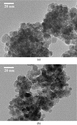 | ||
| Fig. 1 TEM images of (a) pure ZnO and (b) 40% Cd-doped ZnO nanoparticles. | ||
In Raman experiments, Raman scattering light was detected with a Renishaw spectrometer excited at 632.8 nm. Measurements were performed from 0.5 to 2.4 mW for incident laser power, which can avoid sample damage or laser induced heating. No significant spectral change was observed in the range of 0.5 to 2.4 mW for incident laser power. The UV-Visible absorption spectra of the samples were recorded on a Shimadzu UV-Visible Spectrophotometer (UV-2550) using barium sulfate as the standard. A deuterium lamp D2 and a halogen lamp WI served as the excitation sources. The spectrometer was directly linked to a computer by communication cables. The obtained results can be analyzed by the software named UVPROBE in PC client. Photoluminescence (PL) experiments were conducted at room temperature with an excitation source of 325 nm (3.81 eV) He–Cd laser. PL spectra for the samples were detected with a grating monochromator and a standard CCD detection system.
3. Results and discussion
Fig. 2 shows powder X-ray diffraction (XRD) patterns for CdxZn1−xO (x = 0, 0.05, 0.15, 0.40 and 0.80) nanoparticles. For the pure sample, XRD peaks are observed at 2θ = 31.7°, 34.4°, 36.2°, 47.5°, 56.6°, 62.8° and 68.0°, which correspond to (100), (002), (101), (102), (110), (103) and (112) lattice reflection planes of a typical wurtzite structure [JCPDS Card 36-1451]. The intense sharp XRD peaks suggest that the undoped sample has a good crystalline nature. The wurtzite structure is kept up to x = 0.40. It is noted that the XRD bands become broad and blurred with an increase in Cd-doping, indicating a deterioration in crystal quality. When the x-value reaches 0.80, some new peaks are observed at 2θ = 23.5°, 30.4°, 44.0° and 49.9°, as shown by the star marks in Fig. 2, which suggests the appearance of a new phase or phase segregation in the 80% Cd-doped sample. In order to investigate the Cd-doping effect on the lattice parameters of the wurtzite structure for CdxZn1−xO (x = 0, 0.05, 0.15 and 0.40), the (100), (002) and (101) diffraction peaks are fitted with the Gaussian functions. The solid curves in Fig. 3 are the best-fitted results. For the (100) peak, the position shows a slight shift towards a low diffraction angle from 2θ = 31.7° at x = 0 to 31.5° at x = 0.40, and (002) peak shifts from 2θ = 34.4° at x = 0 to 34.0° at x = 0.40, while that for the (110) peak are from 36.2° at x = 0 to 35.7° at x = 0.40. The shifts for the diffraction peaks towards a low diffraction angle indicate lattice expansion in CdxZn1−xO nanoparticles with Cd-doping.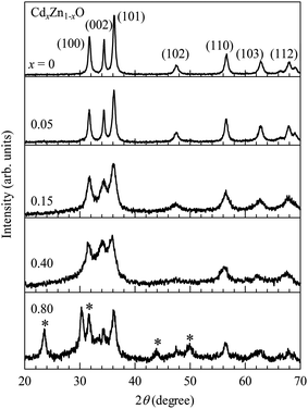 | ||
| Fig. 2 Powder X-ray diffraction (XRD) patterns for CdxZn1−xO (x = 0, 0.05, 0.15, 0.40 and 0.80) nanoparticles. | ||
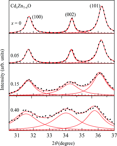 | ||
| Fig. 3 The fitting curves for (100), (002) and (101) diffraction peaks for CdxZn1−xO (x = 0, 0.05, 0.15 and 0.40) nanoparticles by using Gaussian functions. The solid curves are the best-fitted results. | ||
We further calculated the lattice parameters for CdxZn1−xO (x = 0, 0.05, 0.15 and 0.40) nanoparticles. The x dependence of the lattice parameters a and c for CdxZn1−xO nanoparticles are shown in Fig. 4 (a) and (b), respectively. With increasing x, the a-value shows a continuous increase from 3.2453 Å at x = 0 to 3.2623 Å at x = 0.40, while the c-value increases gradually from 5.2036 Å at x = 0 to 5.2173 Å at x = 0.40. The lattice expansion is reasonable because the ionic radius (0.97 Å) of the Cd2+ ion is larger than that (0.74 Å) of the Zn2+ ion. We further calculated the internal parameter u, which shows the deformation ratio for a regular tetrahedron25
| u = (a/c)2/3 + 1/4. | (1) |
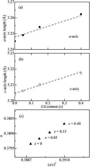 | ||
| Fig. 4 Lattice parameters (a) a and (b) c for CdxZn1−xO (x = 0, 0.05, 0.15 and 0.40) nanoparticles. (c) Relation between structure parameters u and (a/c)2. | ||
The correlation between the internal parameter u and (a/c)2 is shown in Fig. 4(c). The u value for undoped ZnO nanoparticles is 0.3796, which is larger than that (0.3750) for the ZnO single crystal. With an increase in Cd-doping, the u value gradually increases and reaches 0.3803 for x = 0.40. The increase in the u value indicates an enhancement of lattice distortion with Cd-doping, which can be ascribed to the size difference between Cd2+ (0.97 Å) and Zn2+ ions (0.74 Å).
In order to confirm the XRD results, we further investigated the Raman spectra for CdxZn1−xO nanoparticles. ZnO has a wurtzite structure and belongs to the space groupC6v with two formula units in the primitive cell.26 The group theoretical calculation predicts six optical modes: A1 + 2B2 + E1 + 2E2.27 Among them, A1 and E1 modes are active in both Raman and IR while E2 modes are only Raman active, and B2 modes are silent modes. Fig. 5 illustrates the Raman spectra of CdxZn1−xO (x = 0, 0.05, 0.15, 0.40 and 0.80) nanoparticles. For x = 0, a broad peak is found at 438 cm−1, which corresponds to the E2-high mode for ZnO with wurtzite structure.28 With increasing x, the E2 mode shows a significant softening from 438 cm−1 at x = 0 to 424 cm−1 at x = 0.40, suggesting expansion of the Zn–O bond in CdxZn1−xO nanoparticles with Cd-doping.3 In order to compare these results with the XRD results, we also measured the Raman spectra for 80% Cd-doped ZnO nanoparticles and CdO nanoparticles, as shown in Fig. 5 as well. A new peak appears at 260 cm−1 (shown by an upward arrow in Fig. 5) for the 80% Cd-doped sample, which is close to the TO mode of CdO with a rock salt structure. Thus, a new phase or phase segregation occurs in the 80% Cd-doped sample. Therefore, the Raman investigation is consistent with the XRD results.
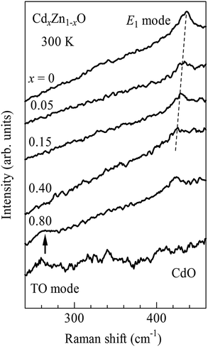 | ||
| Fig. 5 Raman spectra of CdxZn1−xO (x = 0, 0.05, 0.15, 0.40 and 0.80) and CdO nanoparticles. The Raman mode at 438 cm−1 for x = 0 corresponds to the E2-high mode for ZnO with a wurtzite structure. | ||
We then continued to investigate the optical absorption for CdxZn1−xO nanoparticles. Fig. 6 shows the absorption spectra of CdxZn1−xO (x = 0, 0.05, 0.15 and 0.40) nanoparticles. The energy gap Eg of CdxZn1−xO nanoparticles can be obtained with the equation (αhν)2 = B(hν − Eg), where α is the absorption coefficient, hν is the photon energy and B is a function of index of refraction and hole/electron effective masses.29 The broken curves show the best fitted results. The extrapolation of the linear portion of the plot onto the energy axis gives the band gap energy Eg of CdxZn1−xO nanoparticles. The obtained Eg-value decreases as 3.21, 3.18, 3.09 and 2.92 eV for x = 0, 0.05, 0.15 and 0.40, respectively. In doped semiconductors, there is a possibility of widening of the optical band gap due to the Burstein Moss (BM) effect. An enhancement of the band gap was observed in Co-doped ZnO.30 In the present case, the decrease in Eg-value with Cd-doping is not in accordance with the BM effect, which can be attributed to band gap renormalization because the Eg-value (∼2.3 eV) for CdO is smaller than that (∼3.2 eV) for ZnO. A similar effect has been reported for Cd-doped ZnO films.17
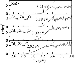 | ||
| Fig. 6 Absorption spectra of CdxZn1−xO (x = 0, 0.05, 0.15 and 0.40) nanoparticles. The gap energy Eg of CdxZn1−xO nanoparticles can be obtained with the equation (αhν)2 = B(hν − Eg). | ||
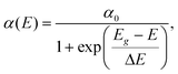
The Urbach band tails were also investigated for CdxZn1−xO (x = 0, 0.05, 0.15 and 0.40) nanoparticles, as shown in Fig. 7. Several factors such as the carrier-impurity interaction, carrier-phonon interaction and structure disorder are responsible for the Urbach band tail in semiconductors.31 We evaluated the Urbach band tails by fitting the absorption coefficient (α) as a function of photon energy (E) in the vicinity of the fundamental absorption edge32
 | (2) |
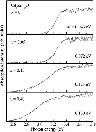 | ||
| Fig. 7 Urbach band tails evaluated by fitting the absorption coefficient α as a function of photon energy in CdxZn1−xO (x = 0, 0.05, 0.15 and 0.40) nanoparticles. | ||
We further investigated the photoluminescence (PL) spectra of CdxZn1−xO (x = 0, 0.05, 0.15 and 0.40) nanoparticles. Fig. 8 displays the PL spectra of the CdxZn1−xO nanoparticles with different Cd content measured at room temperature in the range of 340–750 nm. For the undoped ZnO nanoparticles, two obvious PL bands are observed around 383 nm and 590 nm, respectively. The one around 383 nm is a strong emission band, which originates from a near band-edge (NBE) transition of the wide band gap of ZnO,34 while the other broad band around 590 nm is currently attributed to native defects such as singly ionized oxygen vacancies.35 Compared to the NBE emission band, the intensity of the defect related band is very weak, which indicates that the undoped ZnO nanoparticles have a few defects. With an increase in the x-value up to 0.15, the intensity of the NBE band gradually decreases while the position shows a slight red-shift due to the Cd-doping induced narrowing of the band gap. Simultaneously, the intensity of the broad band increases significantly while the position shows a negligible change. The quenching of the NBE emission and the enhancement of the defect related band indicate that the Cd-doping induced an increase in defects in the samples. When the x-value further increases to 0.40, the intensities for both the PL bands shown suddenly decrease. We have ascribed the suppression of the PL to the non-radiative energy transfers between defect states to lattice. The non-radiative recombination centers should be significantly enhanced in heavy Cd doped ZnO nanoparticles, leading to suppressed PL emission. Similar non-radiative energy transfers have been reported for Eu-doped ZnO nanowires.36 In addition, a weak blue band seems to appear around 450 nm in addition to the red-shifted NBE band when x = 0.40, as shown by a downward arrow in Fig. 8. The new blue PL band may be caused by the defect levels created between the conduction and valence bands such as the shallow donor levels arising from Zn defects.37,38
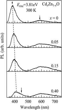 | ||
| Fig. 8 Photoluminescence (PL) spectra of CdxZn1−xO (x = 0, 0.05, 0.15 and 0.40) nanoparticles measured at 300 K in the range of 340–750 nm. | ||
Recently, we have successfully synthesized heavy Mg-doped ZnO nanoparticles by using the sonochemical method. It is found that Mg-doping can significantly increase the gap energy Eg of ZnO nanoparticles, i.e., ∼3.74 eV for Mg0.4Zn0.6O nanoparticles (not shown). Therefore, the energy difference of 0.82 eV between the highest and lowest Eg in doped ZnO nanoparticles is substantially higher than that typically achieved in ZnO nanoparticles by size tuning. We believe that successful doping in the present case is due to the extreme conditions such as high temperature and high pressure under ultrasound irradiation. Thus, the controlling of the ultrasound power and frequency as well as the irradiation time may be important for the synthesis of doped samples with good crystalline quality.
4. Conclusion
We have successfully synthesized heavy Cd-doped ZnO nanoparticles by a sonochemical reaction. X-ray diffraction (XRD) and Raman scattering spectroscopy indicate that the wurtzite structure can be kept in CdxZn1−xO nanoparticles up to x = 0.40. UV-Visible and photoluminescence spectroscopy indicate that both the band gap and the NBE emission band for CdxZn1−xO nanoparticles show red-shift with an increase in Cd-doping. The calculation results on the Urbach band tails reveal an increase in the defects in CdxZn1−xO nanoparticles with Cd incorporation. We further found that the Cd-doping can modify the photoluminescence bands of CdxZn1−xO nanoparticles. Therefore, the sonochemical method is a useful tool for the synthesis of doped nanoparticles.Acknowledgements
This work was supported by NSFC under Grant Nos. 11074124, 11104139 and 10874087, and the National Basic Research Program of China under grant No. 2012CB921504.References
- C. Cheng, R. Xin, Y. Leng, D. Yu and N. Wong, Inorg. Chem., 2008, 47, 7868 CrossRef CAS.
- C. W. Sun, P. Xin, Z. W. Liu and Q. Y. Zhang, Appl. Phys. Lett., 2006, 88, 221914 CrossRef.
- Ü. Özgür, Ya.I. Alivov, C. Liu, A. Teke, M. A. Reshchikov, S. Doğan, V. Avrutin, S.-J. Cho and H. Morkoc, J. Appl. Phys., 2005, 98, 041301 CrossRef.
- X. F. Fan, H. D. Sun, Z. Y. Shen, J.-L. Kuo and Y. M. Lu, J. Phys.: Condens. Matter, 2008, 20, 235221 CrossRef CAS.
- Th. Gruber, C. Kirchner, R. Kling, F. Reuss, A. Waag, F. Bertram, D. Forster, J. Christen and M. Schrek, Appl. Phys. Lett., 2003, 83, 3290 CrossRef CAS.
- F. Bertram, S. Giemsch, D. Forster, J. Christen, R. Kling, C. Kirchner and A. Waag, Appl. Phys. Lett., 2006, 88, 061915 CrossRef.
- F. P. Koffyberg, Phys. Rev. B: Solid State, 1976, 13, 4470 CrossRef CAS.
- K. Sakurai, T. Kubo, D. Kajita, T. Tanabe, H. Takasu, S. Fujita and S. Fujita, Jpn. J. Appl. Phys., 2000, 39, L1146 CrossRef CAS.
- K. Sakurai, T. Takagi, T. Kubo, D. Kajita, T. Tanabe, H. Takasu, S. Fujita and S. Fujita, J. Cryst. Growth, 2002, 237–239, 514 CrossRef CAS.
- S. Shigemori, A. Nakamura, J. Ishihara, T. Aoki and J. Temmyo, Jpn. J. Appl. Phys., 2004, 43, L1088 CrossRef CAS.
- S. Y. Lee, Y. Li, J.-S. Lee, J. K. Lee, M. Nastasi, S. A. Crooker, Q. X. Jia, H.-S. Kang and J.-S. Kang, Appl. Phys. Lett., 2004, 85, 218 CrossRef CAS.
- X. J. Wang, I. A. Buyanova, W. M. Chen, M. Izadifard, S. Rawal, D. P. Norton, S. J. Pearton, A. Osinsky, J. W. Dong and A. Dabiran, Appl. Phys. Lett., 2006, 89, 151909 CrossRef.
- S. Sadofev, S. Blumstengel, J. Cui, J. Puls, S. Rogaschewski, P. Schäfer and F. Henneberger, Appl. Phys. Lett., 2006, 89, 201907 CrossRef.
- C. W. Sun, P. Xin, C. Y. Ma, Z. W. Liu, Q. Y. Zhang, Y. Q. Wang, Z. J. Yin, S. Huang and T. Chen, Appl. Phys. Lett., 2006, 89, 181923 CrossRef.
- J. Ishihara, A. Nakamura, S. Shigemori, T. Aoki and J. Temmyo, Appl. Phys. Lett., 2006, 89, 091914 CrossRef.
- I. A. Buyanova, J. P. Bergman, G. Pozina, W. M. Chen, S. Rawal, D. P. Norton, S. J. Pearton, A. Osinsky and J. W. Dong, Appl. Phys. Lett., 2007, 90, 261907 CrossRef.
- T. Makino, Y. Segawa, M. Kawasaki, A. Ohtomo, R. Shiroki, K. Tamura, K. Tamura, T. Yasuda and H. Koinuma, Appl. Phys. Lett., 2001, 78, 1237 CrossRef CAS.
- R. Triboulet and J. Perrière, Prog. Cryst. Growth Charact. Mater., 2003, 47, 65 CrossRef CAS.
- P. Fons, K. Iwata, S. Niki, A. Yamada, K. Matsubara and M. Watanabe, J. Cryst. Growth, 2000, 209, 532 CrossRef CAS.
- C. Y. Liu and Y. C. Liu, J. Alloys Compd., 2009, 482, 393 CrossRef CAS.
- Y. S. Wang, P. J. Thomas and P. O'Brien, J. Phys. Chem. B, 2006, 110, 21412 CrossRef CAS.
- M. K. Yadav, M. Ghosh, R. Biswas, A. K. Raychaudhuri, A. Mookerjee and S. Datta, Phys. Rev. B: Condens. Matter Mater. Phys., 2007, 76 CrossRef CAS.
- W. E. Mahmoud, A. A. Al-Ghamdia, S. Al-Henitia and S. Al-Ameera, J. Alloys Compd., 2010, 491, 742 CrossRef CAS.
- B. D. Cullity, Elements of X-ray Diffraction, Addison-Wesley, Massachusetts, 1978 Search PubMed.
- H. Schulz and K. H. Thiemann, Solid State Commun., 1979, 32, 783 CrossRef CAS.
- W. L. Bragg, Philos. Mag., 1920, 39, 647 CAS.
- W. G. Fateley, F. R. Dollish, N. T. McDevitt and F. F. Bentley, Infrared and Raman selection rules for molecular and lattice vibrations-the correlation method, Wiley-Interscience, 1972, New York Search PubMed.
- B. Cao, W. Cai, H. Zeng and G. Duan, J. Appl. Phys., 2006, 99, 073516 CrossRef.
- J. I. Pankove, Optical processes in semiconductors. Prentice-Hall, Englewood Cliffs, NJ, 1971 Search PubMed.
- Y. X. Wang, X. Ding, Y. Cheng, Y. J. Zhang, L. L. Yang, H. L. Liu, H. G. Fan, Y. Liu and J. H. Yang, Cryst. Res. Technol., 2009, 44, 517 CrossRef CAS.
- N. B. Chen, H. Z. Wu, D. J. Qiu, T. N. Xu, J. Chen and W. Z. Shen, J. Phys.: Condens. Matter, 2004, 16, 2973 CrossRef CAS.
- W. Badalawa, H. Matsui, T. Osone, N. Hasuike, H. Harima and H. Tabata, J. Appl. Phys., 2011, 109, 053502 CrossRef.
- M. Leroux, N. Grandjean, B. Beaumont, G. Nataf, F. Semond, J. Massies and P. Gibart, J. Appl. Phys., 1999, 86, 3721 CrossRef CAS.
- S. Vijayalakshmi, S. Venkataraj and R. Jayavel, J. Phys. D: Appl. Phys., 2008, 41, 245403 CrossRef.
- K. Vanheusden, C. H. Seager, W. L. Warren, D. R. Tallant and J. A. Voigt, Appl. Phys. Lett., 1996, 68, 403 CrossRef CAS.
- S. Geburt, D. Stichtenoth, S. Müller, W. Dewald, C. Ronning, J. Wang, Y. Jiao, Y. Y. Rao, S. K. Hark and Q. Li, J. Nanosci. Nanotechnol., 2008, 8, 244 CrossRef CAS.
- Z. Fu, B. Lin, G. Liao and Z. Wu, J. Cryst. Growth, 1998, 193, 316 CrossRef CAS.
- R. A. Asmar, S. Juillaguet, M. Ramonda, A. Giani, P. Combette, A. Khoury and A. Foucaran, J. Cryst. Growth, 2005, 275, 512 CrossRef.
| This journal is © The Royal Society of Chemistry 2012 |