Atomic-level control of the thermoelectric properties in polytypoid nanowires†
Sean C.
Andrews‡
ab,
Melissa A.
Fardy‡
ab,
Michael C.
Moore‡
ab,
Shaul
Aloni
b,
Minjuan
Zhang
c,
Velimir
Radmilovic
bd and
Peidong
Yang
*ab
aDepartment of Chemistry, University of California, Berkeley, California 94720, USA
bMaterials Science Division, Lawrence Berkeley National Laboratory, Berkeley, California 94720, USA
cMaterials Research Department, Toyota Research Institute of North America, Toyota Motor Engineering & Manufacturing North America (TEMA) Inc., 1555 Woodridge Avenue, Ann Arbor, Michigan 48105, USA
dNational Center for Electron Microscopy, Lawrence Berkeley National Laboratory, Berkeley, California 94720, USA
First published on 17th January 2011
Abstract
Thermoelectric materials have generated interest as a means of increasing the efficiency of power generation through the scavenging of waste heat. Materials containing nanometer-sized structural and compositional features can exhibit enhanced thermoelectric performance due to the decoupling of certain electrical and thermal properties, but the extent to which these features can be controlled is often limited. Here we report a simple synthesis of M2O3(ZnO)n (M = In, Ga, Fe) nanowires with controllable polytypoid structures, where the nanostructured features are tuned by adjusting the amount of metal precursor. After the introduction of nanometer-scale features (individual atomic layers and alloying), thermal and electrical measurements on single In2-xGaxO3(ZnO)n nanowires reveal a simultaneous improvement in all contributing factors to the thermoelectric figure of merit, indicating successful modification of the nanowire transport properties.
Introduction
The increasing environmental concerns associated with fossil fuel-based energy production have induced a wave of scientific research into affordable alternative energy sources that are both clean and renewable.1 While efforts into green power generation continue in a variety of exciting and promising directions, one avenue that has caught the attention of the scientific community over the past decade is thermoelectrics, wherein electrical power is generated through the scavenging of waste heat. The efficiency of this conversion is related to the material-dependent figure of merit, zT = S2σT/k, where S, σ, T, and k represent the Seebeck coefficient, electrical conductivity, absolute temperature, and thermal conductivity, respectively. Though this has been a topic of scientific study for a number of decades, material engineering directed at maximizing zT has been complicated by the interdependencies of the previously mentioned parameters, limiting the efficiency.2 Specifically, the Seebeck coefficient's inverse dependence on carrier concentration is at odds with the electrical conductivity's direct dependence. An additional problem is that electrons carry both charge and heat, causing a synchronous increase in the electrical and thermal conductivities with carrier concentration. While the interplay of these parameters has limited zT of bulk materials to ∼1 at 300 K, theoretical studies pioneered by Hicks and Dresselhaus predict that it is possible to increase zT by using low dimensional materials, for example, nanowires.3 The enhancement can be attributed to two factors: electronic band structure changes (increasing the Seebeck coefficient) and enhanced interface phonon scattering (reducing the lattice thermal conductivity).4–6 Experimentally, both enhancements have been shown separately in certain nanostructured materials.7–13Superlattices contain periodic compositional and structural features, typically on the nanometer scale,14 making them promising candidates for thermoelectric applications. Early work discovered that bulk In2O3(ZnO)n superlattice structures arise when ZnO is alloyed with high amounts of In, forming layers of InO2− octahedra interspersed between layers of ZnO (002) with near-perfect periodicity.15,16 Later work found that the superlattice-forming materials could be generalized to M2O3(ZnO)n, where M is In, Ga, Fe, and other tri-valent metals, or mixtures such as InGa or InFe.17,18 The increased electrical conductivity from n-type doping and decreased thermal conductivity as a result of interface phonon scattering in the superlattices resulted in a zT of 0.1 across a temperature range of 500–900 K for bulk indium zinc oxide (IZO, In2O3(ZnO)9).19 Previous work on nanowire thermoelectrics suggests that the phononic contribution to thermal transport can be significantly reduced through size reduction and surface engineering.13,20 Therefore, the combination of a superlattice structure and a single-crystalline nanowire could lead to a better phonon-scattering and charge-transporting structure, and hence a better thermoelectric material.21 In this work, we demonstrate a novel method for the rational design and control of nanometer-sized features in the polytypoid M2O3(ZnO)n nanowire system and show an enhancement in zT for indium gallium zinc oxide (IGZO, In2-xGaxO3(ZnO)n) nanowires as a result of these features. Furthermore, we report the first simultaneous improvement in the Seebeck coefficient, electrical conductivity, and thermal resistivity for a nanowire system.
Synthesis of polytypoid oxide nanowires
IZO and IGZO nanowires can be grown by a chemical vapour transport (CVT) method.22–24 However, it remains difficult to achieve rational control over material properties, such as nanowire diameter and dopant concentration, in addition to maintaining a high yield of superlattice wires. Utilizing a three-step, solid-state diffusion process shown schematically in Fig. 1a, we present a novel method for producing M2O3(ZnO)n alloy nanowires that allows for a high level of control in manipulating material composition, structure, and properties. As-grown samples of [002]-oriented ZnO nanowire arrays were first coated with mixtures of In, Ga, and Fe using a thermal evaporation system equipped with a quartz crystal monitor. The metal-coated samples were then annealed at 1173 K in oxygen to form arrays of polytypoid alloy nanowires. The superlattice structure remained after further annealing at 1173 K, indicating that the structure is thermally stable. In this work, samples are referred to by the thickness of the metal coating, rather than the chemical formula, due to the natural distribution of nanowire diameter (affecting concentration) and the polytypoid nature of the nanowires. This method has been applied successfully to synthesize nanowires of IZO, IGZO, gallium zinc oxide (Ga2O3(ZnO)n), and indium iron zinc oxide (In2−xFexO3(ZnO)n) (Figures S1 to S4†).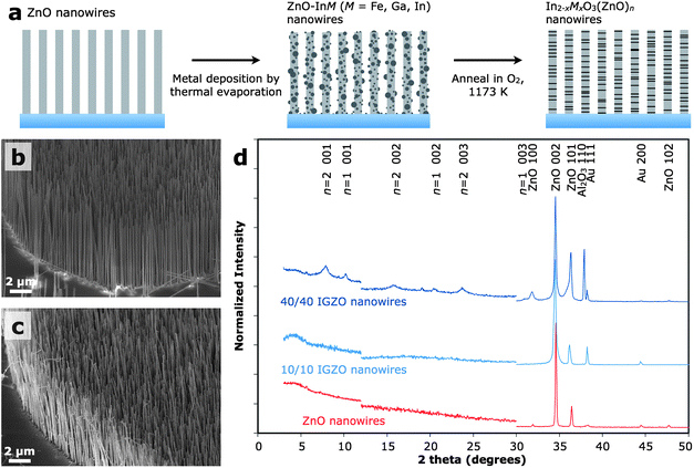 | ||
| Fig. 1 Materials synthesis. (a) Schematic illustration of the synthetic method. (b and c) Scanning electron microscope images of arrays of the as-grown ZnO nanowires (b) and IGZO nanowires prepared with 5/5 nm In/Ga deposition (c). (d) XRD patterns (Cu-Kα irradiation) of ZnO nanowires (bottom) and IGZO nanowires prepared with 10/10 (middle) and 40/40 nm (top) of In and Ga metals. The y-axis was enlarged 5× to highlight low-intensity peaks in the 12–30° region. Longer acquisition times were required below 12° for better signal to noise and thus were normalized separately from the rest of the pattern. | ||
Structural analysis
The solid-state diffusion process used to generate the polytypoid M2O3(ZnO)n nanowires maintains the original morphology of the nanowire array and no etching is observed, as seen in the scanning electron microscope (SEM) images taken before (Fig. 1b) and after (Fig. 1c) alloy formation. The M2O3(ZnO)n nanowires made in this study typically have diameters around 80–130 nm and lengths of 10–15 μm, as determined by the dimensions of the starting ZnO nanowires.25 The strong 002 peak in the X-ray diffraction (XRD) pattern indicates that the nanowire array maintains a vertical orientation after the conversion (Fig. 1d). No In2O3 or Ga2O3 peaks were observed in the IGZO sample made using 10 nm of In and 10 nm of Ga (10/10) deposition, but the weak unidentified peaks in the 40/40 IGZO sample may belong to an alloy of indium and gallium oxide. In the IGZO nanowire alloys, there is little shift from the position of the ZnO nanowire diffraction peaks, but peak broadening towards smaller angles is observed, suggesting the formation of non-uniform alloys. New peaks appear in the low-angle region for the 40/40 IGZO sample, corresponding to spacings of 0.86 and 1.12 nm, which are in good agreement with the predicted lattice constants for M2O3(ZnO)n with n = 1 and n = 2.26Energy dispersive X-ray spectrometry (EDS) confirms the presence of In, Ga, and Zn in the IGZO nanowires (Figure S2†), with an In![[thin space (1/6-em)]](https://www.rsc.org/images/entities/char_2009.gif) :Ga atomic ratio of approximately 1:1. The relative amounts of In and Ga compared to Zn varies depending on the diameter of the starting ZnO nanowire.
:Ga atomic ratio of approximately 1:1. The relative amounts of In and Ga compared to Zn varies depending on the diameter of the starting ZnO nanowire.
Transmission electron microscope (TEM) images of 10/10 IGZO nanowires (Fig. 2a) show a modulation in contrast along their longitudinal axis, which can be attributed to a superlattice structure. According to previous reports, the superlattice structure consists of planes of InO2−octahedra separated by slabs of wurtzite MZnnO(n+1)+ (M = In, Ga).16 To confirm the structure of our nanowires, Z-contrast scanning transmission electron microscopy (STEM) imaging was done using a 300 kV double-Cs-corrected STEM capable of 50 pm resolution. In Z-contrast images, the intensity is approximately proportional to the mean square of the atomic number of the constituent atoms. Thus, using Z-contrast imaging, the position of In (Z = 49) can be unambiguously determined, but Ga (Z = 31) and Zn (Z = 30) cannot be distinguished from one another since their atomic numbers differ by only one. Oxygen cannot be imaged due to its relatively small atomic number. Fig. 2b is a Z-contrast image of a 10/10 IGZO nanowire clearly showing the presence of In-enriched layers (brightest lines) oriented perpendicular to the [002] direction. As observed in the high-resolution (HR)-STEM image in Fig. 2c, the In atoms sit on individual planes and are separated by wurtzite MZnnO(n+1)+ slabs of varying thickness (Fig. 2c). Only single layers of In atoms were observed in the 10/10 IGZO nanowires, consistent with the layers being composed of octahedrally-coordinated InO2−, which has been shown to be the most stable configuration for In within the superlattice structure.26EDS mapping suggests that Ga may also be present in the octahedral layers, indicating that their true composition is In1−xGaxO2− (Figure S5†).
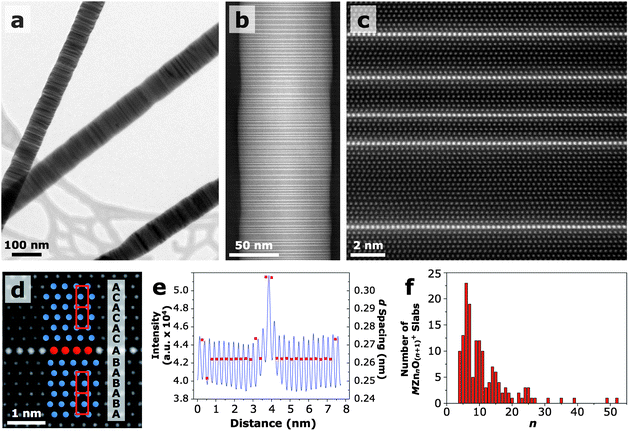 | ||
| Fig. 2 Transmission electron microscopy. (a) TEM image of multiple IGZO nanowires. (b) Z-contrast STEM image of a 10/10 IGZO nanowire. The Z contrast in the image clearly shows that In atoms are preferentially located within layers oriented perpendicularly to the nanowire growth direction. (c) HRSTEM image of an IGZO nanowire showing individual MO2− layers sandwiched between multiple MZnnO(n+1)+ layers. (d) HRSTEM image highlighting the change in stacking sequence across a MO2− layer. (e) Intensity line profile and d spacing across a MO2− layer taken from a HRSTEM image. On either side of the inclusion, the d spacing shows an expansion of ∼17% relative to that of pure ZnO. (f) Frequency of different n values of the MZnnO(n+1)+ layers measured from HRSTEM images of several 10/10 IGZO nanowires. The average n is 11 and the most frequent is 6. | ||
The O atoms on the edges of the MO2− octahedral layers are each bonded to three In/Ga atoms and one metal atom within the MZnnO(n+1)+ layer.26 This creates an inversion domain boundary (IDB) in the wurtzite lattice since the Zn–O bonds on either side of the octahedral layer point with the O atoms toward the In/Ga layer (tail-to-tail configuration). The MO2− inclusion layer is also associated with a stacking fault, which together with the IDB produces an AaBbAaBbAcCaAcCaA (capital and lowercase letters correspond to metal and oxygen atoms, respectively) stacking sequence in which the wurtzite lattice on one side of the In/Ga layer is translated by 1/3<100> (Fig. 2d). The location of the octahedral MO2− within the stacking sequence is denoted by the bold bAc.
The presence of the IDB at the octahedral layer means that the polarity of the ZnO must revert somewhere within the MZnnO(n+1)+ slab to produce the necessary tail-to-tail polarity at the adjacent MO2− layer. There are several proposed mechanisms by which the polarity can be reverted.15,26–28 Yan et al. reported the presence of mirror domain boundaries (MDB) within the ZnO slabs of their IZO films.15 However, no such boundaries could be seen in our IGZO nanowires. An additional layer of In atoms within the MZnnO(n+1)+ slabs may also act as an IDB. The M and Zn atoms within the MZnnO(n+1)+ layer occupy the tetrahedral or trigonal bipyramidal sites,16,29 and those with 5-fold coordination may be ordered in either flat layers or zigzag layers.26,28,30 Using density functional theory (DFT) calculations Yan et al. and Da Silva et al. compared the relative energies of these two structures and found that the zigzag modulated structure is more stable for a number of reasons. Firstly, in the zigzag layer, O has an energetically favourable tetrahedral coordination, while in the flat layer O has a coordination of three.28 Also, the occupation of the trigonal bipyramidal sites within the wurtzite lattice can cause local lattice distortions and strain within the MZnnO(n+1)+ slabs. This strain can be reduced by localizing the atoms with trigonal bipyramidal coordination to one boundary. The zigzag layer was found to most effectively reduce this strain.26,28 Zigzags were seen in all four types of alloys synthesized in this study (Figs. S1 to S4†), but were not apparent in those alloys with small n. Also, since the trigonal bipyramidal sites may be occupied by In, Ga, or Zn atoms in the IGZO nanowires, the zigzags appear faint in the Z-contrast images and in some cases are not discernable. A previous report observed that zigzags are only present in superlattices with n > 6.29 The lattice strain caused by a flat layer of trigonal bipyramidally coordinated In/Ga atoms decreases as the thickness of the MZnnO(n+1)+ slabs decreases, so the energy difference between the flat and zigzag configurations decreases with decreasing n.26 Therefore, it is conceivable that the polarity of the MZnnO(n+1)+ layers with small n may be reversed via a flat layer of trigonal bipyramidal atoms.
In agreement with XRD, the d spacings in the MZnnO(n+1)+ layers (Fig. 2e) are unchanged from (002) in pure ZnO (0.262 nm), but the octahedral MO2− planes force a local 17% increase in the d spacing (0.307 nm) on either side of the inclusion layers (subscripts denote numbers beyond the significant figures). The d spacings were determined by taking an intensity line profile across an In/Ga inclusion in a HRSTEM image and measuring the distance between peaks. This change in d spacing on either side of the In/Ga inclusions corresponds with that reported by Yan et al. and Jie et al. on IZO.15,22 This significant increase in d spacing around the inclusion layer is associated with a large amount of lattice strain.
To approximate an n value for the 10/10 IGZO nanowires, the number of atomic layers in each MZnnO(n+1)+ slab was counted for several nanowires (Fig. 2f). The average n is 11, but the most frequent is 6. Some n values, such as n = 8, are only represented by a small number of MZnnO(n+1)+ slabs. The reason for this is presently unknown and requires further study. n can be related to the spacing (![[small script l]](https://www.rsc.org/images/entities/i_char_e146.gif) ) between MO2− layers by the following equation:
) between MO2− layers by the following equation:
| (nm) = 0.614 + 0.262n | (1) |
The amount of metal deposition was varied to determine its effect on MO2− layer density (Fig. 3, a to d). The surface of the 40/40 IGZO nanowire shown in Fig. 3d appears rough due to the presence of oxide particles left over after the solid-state diffusion process. However, most IGZO nanowires in the sample did not show surface particles. Line intensity profiles drawn perpendicular to the MO2− inclusions were used to generate power spectra (Fig. 3, e to h) from the nanowires shown in Fig. 3, a to d. The power spectra show the most common frequencies (1/) within the nanowires, providing information regarding the MO2− layer spacings and the periodicity of the spacings. As the thickness of metal deposition is increased the most common frequencies shift to higher 1/ (smaller ) indicating that the distance between MO2− layers decreases with increased metal deposition. The periodicity also increases with metal deposition, which can be seen in the emergence of distinct peaks, such as in Fig. 3g and 3h. The frequencies obtained from the 10/10 power spectrum match the n values that were directly counted in Fig. 2d. As seen in Fig. 3h, the majority of MO2− layers in the 40/40 IGZO are separated by 2 or 3 layers of MZnnO(n+1)+, which is supported by the low-angle XRD pattern (Fig. 1d) and the HRSTEM image taken from same 40/40 IGZO nanowire sample (Figure S6†). It is evident from these power spectra that both n and the superlattice periodicity can be controllably tuned by adjusting the amount of metal deposition.
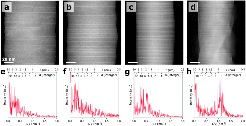 | ||
| Fig. 3 Atomic-level control. (a to d) Z-contrast STEM images of IGZO nanowires prepared with 10, 20, 40, and 80 nm of metal (1:1 of In:Ga by film thickness), respectively. (e to h) Power spectra generated using line intensity profiles drawn along the length of the nanowires showing the frequency of reciprocal distance between MO2− layers for (a to d). The distance between MO2− layers decreases with increasing thickness of metal deposition. The periodicity of the MO2− layer spacings also improves. | ||
Mechanism
The ability to control the MO2− inclusion density is a direct result of the solid-state diffusion process by which the polytypoid nanowires are produced. The diffusion rates of In, Ga, and Zn within ZnO are extremely high at the 1173 K annealing temperature, with values of 6.62 × 10⁻¹², 1.09 × 10⁻¹⁴, and 1.13 × 10⁻¹² cm2s−1, respectively.31,32 DFT calculations show that Zn atoms diffuse through ZnO using Zn vacancies.33 Based on their activation energies for diffusion, In and Ga are also thought to diffuse through Zn vacancies, though some controversy exists regarding their true activation energies.31,34,35 Since In and Ga are substitutional dopants, Zn atoms must diffuse out when the In and Ga atoms diffuse in. The Zn atoms diffuse to the surface of the nanowire, leading to a modulation in the diameter (Fig. 4a). In areas of higher inclusion density, the diameter of the nanowire is slightly thicker (more In and Ga diffused in, more Zn diffused out) compared to areas of lower inclusion density.![Partial octahedral layers. (a) Z-contrast STEM image of a 10/10 IGZO nanowire showing diameter fluctuations with inclusion density. The arrows indicate the presence of partial inclusions, all of which are connected to one side of the nanowire. (b) HRSTEM image of IGZO oriented on the [010] zone axis with two incomplete MO2−layers and the corresponding FFT (inset). (c and d) Moiré images takes along the 002 (b) and 102 (c) reflections clearly showing the presence of edge dislocations at the end of each incomplete MO2− layer.](/image/article/2011/SC/c0sc00537a/c0sc00537a-f4.gif) | ||
| Fig. 4 Partial octahedral layers. (a) Z-contrast STEM image of a 10/10 IGZO nanowire showing diameter fluctuations with inclusion density. The arrows indicate the presence of partial inclusions, all of which are connected to one side of the nanowire. (b) HRSTEM image of IGZO oriented on the [010] zone axis with two incomplete MO2−layers and the corresponding FFT (inset). (c and d) Moiré images takes along the 002 (b) and 102 (c) reflections clearly showing the presence of edge dislocations at the end of each incomplete MO2− layer. | ||
Once the In and Ga diffuse into the nanowire, they strain the wurtzite lattice of the pure ZnO, deforming the structure, and eventually relaxing the strain by creating octahedral In/Ga inclusions and trigonal bipyramidal layers. Defects such as edge dislocations, stacking faults, and inversion domain boundaries are known to attract impurities and can assist in the formation of impurity inclusions.36 In some of the nanowires synthesized in this study, especially those made with lower amounts of In and Ga, partial In/Ga inclusions were observed (Fig. 4b–d). The ends of these partial inclusions are usually associated with edge dislocations with the dislocation line lying at the leading edge of the MO2− plane.37 Edge dislocations can be seen in Fig. 4b in the HRSTEM image of two partial inclusions. Moiré images taken along the 002 and 102 reflections clearly show the presence of the edge dislocations. Another interesting observation is that the partial inclusions are always connected to one surface of the nanowire (Fig. 4a), indicating that the growth of the inclusion starts at the surface and proceeds across the diameter of the nanowire until it either reaches the opposite side or connects with an inclusion growing from the opposite side (Figure S7†).
If the inclusions are growing through a defect-assisted process and the inclusion formation begins at the nanowire surface, then the edge dislocation must somehow nucleate near the surface. One possible scenario is that the edge dislocations are formed on the nanowire surface via heterogeneous nucleation, which occurs with the help of defects such as impurity atoms. Since In has a larger ionic radius compared to Zn, the dissolution of In within the wurtzite lattice will create strain. The presence of dislocations within the lattice can relax some of this strain if the In atoms diffuse towards the dislocations and eventually occupy those lattice positions below the edge dislocations where the lattice is already expanded. The edge dislocation basically creates a “hole” in which the larger In atoms can sit. Due to the high diffusion rate of In within the ZnO lattice, the In atoms can rapidly concentrate at the sites of edge dislocations. Since the In atoms have a mutual attraction they can crystallize into another phase (octahedrally coordinated MO2−) which will flow in one direction towards the dislocation. The growth of the inclusion will continue along the dislocation until the concentration of In within the lattice decreases to the point at which equilibrium is reached. In the lower concentration samples, more partial inclusions can be observed, likely resulting from insufficient quantities of In atoms necessary to complete the inclusions. In 40/40 IGZO, no partial inclusions were observed.
Electrical modification
The presence of the MO2− inclusions alters both the thermal and electrical properties in the converted polytypoid nanowires. While ZnO can exhibit a relatively high intrinsic electrical conductivity due to formation of oxygen vacancies acting as donor states, the introduction of slight amounts of Al, In, or Ga can further increase the conductivity when substituted for Zn.38 Considering all the M2O3(ZnO)n nanowires synthesized in this study, the high inclusion density and significant dopant level present in the IGZO nanowires makes them the ideal candidate for thermoelectric enhancement, and thus, IGZO nanowires were used for all transport studies. The increased electrical conductivity observed at room temperature in the IGZO nanowires when compared to the ZnO nanowires is consistent with that of a slightly doped semiconductor (Fig. 5a). However, considering the relatively large amount of In and Ga incorporation (greater than 2% atomic of each metal atom from EDS), the observed increase in conductivity is smaller than the metallic-like value of conduction that is expected. While the In and Ga impurities can act as electrical dopants in ZnO when substituted for tetrahedrally-coordinated Zn, In and Ga also sit in the trigonal bipyramidal sites, helping to preserve electroneutrality and reducing the number of generated carriers. Moreover, the MO2− inclusions can act as barriers to oxygen diffusion leading to decreased conductivity by suppressing the formation of oxygen vacancies.39 Interestingly, the linear temperature-dependent resistance of IGZO, as seen in Fig. 5a, is not typical behaviour for a slightly doped semiconductor (of which pure ZnO nanowires are an example) nor of a degenerately doped semiconductor (which should give metallic behaviour). This deviation from the classical semiconducting behaviour indicates a departure from the typical thermally-activated mechanism. The octahedral layers could be acting as potential barriers to electron diffusion, leading to alternative transport mechanisms such as pseudo variable-range hopping or percolation conduction.40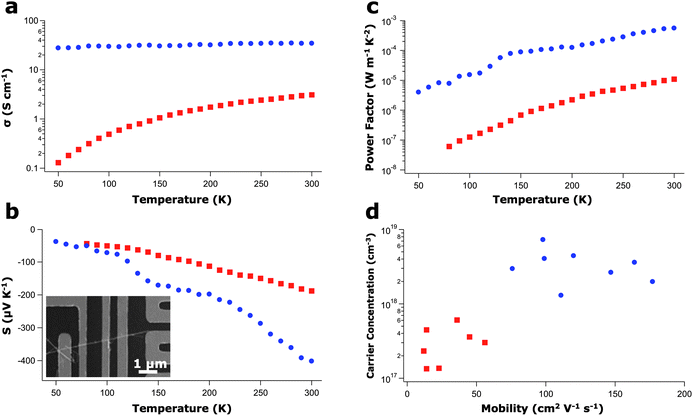 | ||
| Fig. 5 Single-wire electrical measurements. (a) Electrical conductivity as a function of temperature for a 120-nm diameter 5/5 IGZO nanowire (blue circles) and a 110-nm diameter ZnO nanowire (red squares). (b and c) Seebeck coefficient (b) and power factor (c) as a function of temperature measured for the same nanowires in (a). Inset shows a SEM of an individual nanowire in a four-point FET/Seebeck device. (d) Carrier concentration as a function of mobility, as measured from the FET geometry. No diameter dependence was observed for ZnO or IGZO nanowires in the range of 75–130 nm. | ||
The presence of the inclusion layers also has an effect on the induced Seebeck voltage, as seen in Fig. 5b. At 300 K, the Seebeck coefficient grew in magnitude from −188 μV K−1 in ZnO nanowires to −402 μV K−1 in IGZO nanowires. Similar Seebeck values were observed in each of the many ZnO and IGZO nanowire samples measured, respectively. The observed increase in Seebeck coefficient may be an effect of the potential barriers, which could act as low-energy electron filters.41 When a temperature gradient is applied, charges diffuse to states of lower chemical potential. While most of these states are on the colder side, unoccupied states on the hotter side allow for charge diffusion in the opposing direction, thereby limiting the overall potential that can develop for a given temperature gradient. Charges that participate in back diffusion are referred to as “cold electrons” (for n-type semiconductors) since they posses lower carrier energy. However, potential barriers with appropriate energy levels can act as low energy charge filters by preferentially affecting their mobility.42 By limiting the amount of back diffusion, a larger potential can develop, resulting in an increased Seebeck coefficient.
Aside from filtering, the possibility exists that electronic quantum confinement caused by closely spaced inclusion layers contributes to the rise in Seebeck values.3,43 Since values of less than 2.34 nm (exciton Bohr radius of ZnO) were observed, thermopower enhancement might be due to slight changes in the density of states near the Fermi level.44 While difficult to quantify at this time, the random nature of the single crystalline, polytypoid nanowires perhaps plays a role in these and other transport phenomena. Further theoretical and experimental investigations are required in order to paint a clearer picture of this nanowire system.
Regardless of the source of enhancement, by converting the ZnO nanowires into IGZO, the resulting power factor (S2σ) changed by a factor of 58 to 0.6 mW m−1K−2. While this value is lower than the reported power factor of nominally Al-doped ZnO,45 it is ∼6 times larger than the power factor of bulk IZO materials (Fig. 5c).46 The complete thermoelectric properties for bulk IGZO have not been reported in a single study, so while the comparison of the IGZO nanowires with bulk IGZO is more relevant, the transport properties within this work are primarily given relative to the similarly structured bulk IZO.
Carrier mobility enhancement
To ensure that the observed Seebeck enhancement is not due to mere increases in impurity scattering, FET mobilities were measured on the same nanowires from which the electrical conductivity and Seebeck coefficient were determined (Fig. 5d). Both carrier concentration and mobility enhancements were observed when compared to the pure ZnO nanowires. This indicates that the carrier concentration, and not the mobility, is the limiting factor in the electrical conductivity, contrary to what may have been suspected based on the defects that accompany each MO2− layer. Furthermore, 177 cm2 V−1s−1 at 300 K is more than twice the field effect mobility value previously measured in single crystalline IGZO thin films.39 The nature of the mobility enhancement in the polytypoid IGZO nanowires over IGZO thin films is not fully understood. However, the enhancement over the single crystalline ZnO nanowires may be explained by the induced strain at the MO2− layer interfaces. It is well established that piezoresistive materials, both crystalline and amorphous, demonstrate mobility changes with the application of stress.47,48 As seen in Fig. 2e, the 17% difference in the d spacing at the octahedral/wurtzite interface produces a significant amount of strain. Although the inclusions are perpendicular to the transport direction, the mobility could be enhanced by possible strain-induced changes to the electronic band structure. Further theoretical and experimental work is necessary to determine the extent to which strain plays a role in this polytypoid system.Thermal conductivity reduction
Not only do the nanostructured features influence electronic transport, they also act as important phonon scattering interfaces, thereby limiting the lattice thermal conductivity.49 Compared to literature values for bulk ZnO (100 W m−1 K−1), ZnO nanowires demonstrate up to five-fold reduction of thermal conductivity at room temperature (Fig. 6b).50 An estimation of the average phonon mean free path as a function of temperature shows that the limiting factor is the nanowire diameter until the 150–200 K range, where other scattering mechanisms, such as impurity and umklapp scattering, begin to limit the conductivity. As seen in Fig. 6b, the linear segment of the ZnO nanowire plot begins to plateau around that temperature range. The IGZO nanowires, on the other hand, show no such plateau, indicating that the MO2− layers, and not to the nanowire diameter, are limiting the average phonon mean free path throughout the measured temperature range. At 300 K, IGZO nanowires exhibit a thermal conductivity of 3.3 W m−1 K−1, which is only slightly lower than what has been observed for IZO in the bulk (3.5 W m−1 K−1, n = 3,4).51 However, since bulk IZO has both higher inclusion density and periodicity, it is surprising that the more disordered 5/5 IGZO nanowires exhibit comparable thermal transport properties. While higher inclusion densities are expected to limit the average phonon mean free path, the disordered nature of the polytypoid IGZO structure combined with the nanowire geometry similarly affects the overall thermal energy propagation, as seen in other systems.52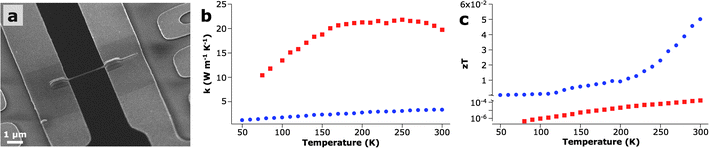 | ||
| Fig. 6 Thermoelectric measurements. (a) SEM of an individual IGZO nanowire bridging two suspended membranes on a prefabricated MEMS device used for thermal conductivity measurements. (b) Thermal conductivity as a function of temperature for both a 120-nm 5/5 IGZO nanowire and a 90-nm ZnO nanowire. (c) Figure of merit, zT, of IGZO nanowires compared with ZnO nanowires showing an enhancement of 2.5 orders of magnitude after alloying. | ||
As a direct result of the polytypoid structure, zT was increased from 1.7 × 10⁻⁴ for ZnO nanowires to 0.055 for the IGZO nanowires at 300 K, an enhancement of 2.5 orders of magnitude (Fig. 6c). Such zT values represent a factor of ∼10 enhancement when compared to the similarly structured bulk IZO superlattice samples.51,53 However, since oxide-based thermoelectric modules are typically employed at elevated temperatures (700–1000 K), further studies within the relevant temperature range are required.
Conclusion
In summary, M2O3(ZnO)n (M = In, Ga, Fe) polytypoid nanowires were converted from pure ZnO nanowires using a facile diffusion scheme. This solid-state diffusion process can be used to produce a wide range of ZnO alloys with controllable alloy concentration and inclusion layer density. The inclusion growth is believed to originate from the surface and propagate though the nanowire by a defect-assisted process. Single-nanowire measurements on IGZO show that both the power factor and thermal resistivity were enhanced due to the nanostructured features inherent to this thermally stable system. In addition, compared to bulk IZO and other doped ZnO, IGZO nanowires show a marked improvement in zT at room temperature. Based on this study, we suggest that better control of nanometer-scale features (nanowire geometry, alloying, atomic layer inclusions) could be the key to developing next-generation thermoelectric materials.Methods
ZnO nanowires were grown on sapphire (110) substrates using a Au-catalyzed chemical vapor transport process.25 Typical nanowires had diameters of 80–130 nm and lengths of 10–15 μm. A home-built thermal evaporation system was used to deposit varying amounts of In, Ga, and Fe metals as measured by the film thickness of evaporated metal incident on a quartz crystal monitor. By monitoring the thickness of the deposited metal it was possible to generate reproducible alloy concentrations and control metal ratios in mixed depositions. The metal-coated ZnO nanowire substrates were loaded into the center of a 1-inch diameter quartz tube and heated in a tube furnace under an O2 atmosphere at 1173 K for 12–96 h. This method was used to synthesize IZO (Figure S1†), IGZO (Figure S2†), gallium zinc oxide (Figure S3†), and indium iron zinc oxide (IFZO) (Figure S4†) nanowires.IGZO nanowires were prepared using different thicknesses of In/Ga metal coatings over a range of 5/5 nm to 40/40 nm. For loadings greater than 10/10 nm, samples were prepared using successive coatings of In and Ga. Thermoelectric measurements focused on IGZO nanowires prepared from combined 5 nm In and 5 nm Ga coatings on ZnO nanowires.
Electrical devices were made by either drop-casting or micro-manipulating nanowires onto a Si chip with 200 nm of thermal oxide on the surface. The nanowires were top-contacted using metallic contacts defined by standard photolithography techniques. Ti/Au was used as the contact and Ohmic contact was achieved after rapid thermal annealing. Seebeck coefficients were determined by measuring the thermal voltage induced by passing current through a heating coil near the nanowire. The contacts where used as resistive thermometers to measure the temperature difference across the nanowire. Thermal transport in individual nanowires was accomplished using pre-fabricated MEMS devices, upon which single nanowires were physically manipulated using thin tungsten probe tips. Full descriptions of the measurement scheme can be found elsewhere.54
Acknowledgements
This work was supported the Director, Office of Basic Energy Sciences, Materials Sciences and Engineering Division, of the U.S. Department of Energy under Contract No. DE-AC02-05CH11231. Early stages of materials synthesis were supported by Toyota, later stages of materials synthesis and characterization were supported by DOE. P.Y. would like to thank NSF for the A.T. Waterman Award. We thank National Center of Electron Microscopy for the use of their facilities.References
- A. I. Hochbaum and P. Yang, Semiconductor nanowires for energy conversion, Chem. Rev., 2010, 110, 527–546, DOI:10.1021/cr900075v.
- G. J. Snyder and E. S. Toberer, Complex thermoelectric materials, Nat. Mater., 2008, 7, 105–114, DOI:10.1038/Nmat2090.
- L. D. Hicks and M. S. Dresselhaus, Thermoelectric figure of merit of a one-dimensional conductor, Phys. Rev. B: Condens. Matter, 1993, 47, 16631 CrossRef CAS.
- D. Donadio and G. Galli, Atomistic simulations of heat transport in silicon nanowires, Phys. Rev. Lett., 2009, 102, 4, DOI:10.1103/PhysRevLett.102.195901.
- J. H. Lee, G. A. Galli and J. C. Grossman, Nanoporous Si as an efficient thermoelectric material, Nano Lett., 2008, 8, 3750–3754, DOI:10.1021/nl802045f.
- P. Martin, Z. Aksamija, E. Pop and U. Ravaioli, Impact of phonon-surface roughness scattering on thermal conductivity of thin Si nanowires, Phys. Rev. Lett., 2009, 102, 125503 CrossRef.
- T. C. Harman, P. J. Taylor, M. P. Walsh and B. E. LaForge, Quantum dot superlattice thermoelectric materials and devices, Science, 2002, 297, 2229–2232 CrossRef CAS.
- A. I. Boukai, et al. Silicon nanowires as efficient thermoelectric materials, Nature, 2008, 451, 168–171, DOI:10.1038/nature06458.
- B. Poudel, et al. High-thermoelectric performance of nanostructured bismuth antimony telluride bulk alloys, Science, 2008, 320, 634–638, DOI:10.1126/science.1156446.
- J. P. Heremans, et al. Enhancement of thermoelectric efficiency in PbTe by distortion of the electronic density of states, Science, 2008, 321, 554–557, DOI:10.1126/science.1159725.
- H. Bottner, G. Chen and R. Venkatasubramanian, Aspects of thin-film superlattice thermoelectric materials, devices, and applications, MRS Bull., 2006, 31, 211–217.
- K. F. Hsu, et al. Cubic AgPb mSbTe2+m: Bulk thermoelectric materials with high figure of merit, Science, 2004, 303, 818–821 CrossRef CAS.
- A. I. Hochbaum, et al. Enhanced thermoelectric performance of rough silicon nanowires, Nature, 2008, 451, 163–167, DOI:10.1038/Nature06381.
- C.-Y. Wen, et al. Formation of Compositionally Abrupt Axial Heterojunctions in Silicon-Germanium Nanowires, Science, 2009, 326, 1247–1250, DOI:10.1126/science.1178606.
- Y. Yan, et al. Polytypoid structures in annealed In2O3-ZnO films, Appl. Phys. Lett., 1998, 73, 2585–2587 CrossRef CAS.
- N. Kimizuka, M. Isobe and M. Nakamura, Syntheses and single-crystal data of homologous compounds, In2O3(ZnO)m (m = 3, 4, and 5), InGaO3(ZnO)3, and Ga2O3(ZnO)m (m = 7, 8, 9, and 16) in the In2O3–ZnGa2O4–ZnO system, J. Solid State Chem., 1995, 116, 170–178 CrossRef CAS.
- T. Horlin, G. Svensson and E. Olsson, Extended defect structures in zinc oxide doped with iron and indium, J. Mater. Chem., 1998, 8, 2465–2473 RSC.
- C. F. Li, Y. Bando, M. Nakamura and N. Kimizuka, Antiphase modulated structure of Fe2O3(ZnO)15 studied by high-resolution electron microscopy, J. Solid State Chem., 1999, 142, 174–179 CrossRef CAS.
- H. Ohta, W. S. Seo and K. Koumoto, Thermoelectric properties of homologous compounds in the ZnO-In2O3 system, J. Am. Ceram. Soc., 1996, 79, 2193–2196 CAS.
- D. Li, Y. Wu, R. Fan, P. Yang and A. Majumdar, Thermal conductivity of Si/SiGe superlattice nanowires, Appl. Phys. Lett., 2003, 83, 3186–3188 CrossRef CAS.
- Y. Lin and M. Dresselhaus, Thermoelectric properties of superlattice nanowires, Phys. Rev. B: Condens. Matter, 2003, 68, 075304, DOI:10.1103/PhysRevB.68.075304.
- J. S. Jie, G. Z. Wang, X. H. Han and J. G. Hou, Synthesis and characterization of ZnO: In nanowires with superlattice structure, J. Phys. Chem. B, 2004, 108, 17027–17031, DOI:10.1021/Jp0484783.
- C. W. Na, S. Y. Bae and J. Park, Short-period superlattice structure of Sn-doped In2O3(ZnO)4 and In2O3(ZnO)5 nanowires, J. Phys. Chem. B, 2005, 109, 12785–12790, DOI:10.1021/Jp0442246.
- D. P. Li, G. Z. Wang, Q. H. Yang and X. Xie, Synthesis and photoluminescence of InGaO3(ZnO) m nanowires with perfect superlattice structure, J. Phys. Chem. C, 2009, 113, 21512–21515, DOI:10.1021/jp906381h.
- M. H. Huang, et al. Room-temperature ultraviolet nanowire nanolasers, Science, 2001, 292, 1897–1899 CrossRef CAS.
- J. L. F. Da Silva, Y. F. Yan and S. H. Wei, Rules of structure formation for the homologous InMO3(ZnO)n compounds, Phys. Rev. Lett., 2008, 100, 255501, DOI:10.1103/Physrevlett.100.255501.
- Y. Ding, X. Y. Kong and Z. L. Wang, Doping and planar defects in the formation of single-crystal ZnO nanorings, Phys. Rev. B: Condens. Matter Mater. Phys., 2004, 70, 235408 CrossRef.
- Y. Yan, J. L. F. Da Silva, S.-H. Wei and M. Al-Jassim, Atomic structure of In2O3–ZnO systems, Appl. Phys. Lett., 2007, 90, 261904–261903 CrossRef.
- C. Li, Y. Bando, M. Nakamura and N. Kimizuka, A modulated structure of ln2O3(ZnO)m as revealed by high-resolution electron microscopy, J. Electron Microsc., 1997, 46, 119–127 CAS.
- M. Isobe, N. Kimizuka, M. Nakamura and T. Mohri, Structures of LuFeO3(ZnO)m (m = 1, 4, 5 and 6), Acta Crystallographica Section C, 1994, 50, 332–336, DOI:10.1107/S0108270193008108.
- D. G. Thomas, The diffusion and precipitation of indium in zinc oxide, J. Phys. Chem. Solids, 1959, 9, 31–42 CrossRef CAS.
- I. Broser et al. Physics of II–VI and I–VII Compounds, Semimagnetic Semiconductors. Vol. 17 (Springer-Verlag, 1982) Search PubMed.
- P. Erhart and K. Albe, Diffusion of zinc vacancies and interstitials in zinc oxide, Appl. Phys. Lett., 2006, 88, 201918–201913 CrossRef.
- T. Nakagawa, et al. Analysis of indium diffusion profiles based on the Fermi-level effect in single-crystal zinc oxide, Jpn. J. Appl. Phys., 2008, 47, 7848 CrossRef CAS.
- T. Nakagawa, et al. Diffusion model of gallium in single-crystal ZnO proposed from analysis of concentration-dependent profiles based on the Fermi-level effect, Jpn. J. Appl. Phys., 2007, 46, 4099 CrossRef CAS.
- G. Popovici, et al. Impurity contamination of GaN epitaxial films from the sapphire, SiC and ZnO substrates, Appl. Phys. Lett., 1997, 71, 3385–3387 CrossRef CAS.
- C. Li, Y. Bando, M. Nakamura and N. Kimizuka, Relation between In ion ordering and crystal structure variation in homologous compounds InMO3(ZnO)m (M = Al and In; m = integer), Micron, 2000, 31, 543–550 CrossRef CAS.
- G.-D. Yuan, et al. Tunable n-type conductivity and transport properties of Ga-doped ZnO nanowire arrays, Adv. Mater., 2008, 20, 168–173 CrossRef CAS.
- K. Nomura, et al. Thin-film transistor fabricated in single-crystalline transparent oxide semiconductor, Science, 2003, 300, 1269–1272 CrossRef CAS.
- K. Nomura, et al. Carrier transport in transparent oxide semiconductor with intrinsic structural randomness probed using single-crystalline InGaO3(ZnO)5 films, Appl. Phys. Lett., 2004, 85, 1993–1995, DOI:10.1063/1.1788897.
- A. Shakouri, E. Lee, D. Smith, V. Narayanamurti and J. Bowers, Thermoelectric effects in submicron heterostructure barriers, Nanoscale Microscale Thermophys. Eng., 1998, 2, 37–47 Search PubMed.
- L. W. Whitlow and T. Hirano, Superlattice applications to thermoelectricity, J. Appl. Phys., 1995, 78, 5460–5466 CrossRef CAS.
- H. Ohta, R. Huang and Y. Ikuhara, Large enhancement of the thermoelectric Seebeck coefficient for amorphous oxide semiconductor superlattices with extremely thin conductive layers, Phys. Status Solidi RRL, 2008, 2, 105–107, DOI:10.1002/pssr.200802017.
- R. Senger and K. Bajaj, Optical properties of confined polaronic excitons in spherical ionic quantum dots, Phys. Rev. B: Condens. Matter, 2003, 68, 045313, DOI:10.1103/PhysRevB.68.045313.
- T. Tsubota, M. Ohtaki, K. Eguchi and H. Arai, Thermoelectric properties of Al-doped ZnO as a promising oxide material for high-temperature thermoelectric conversion, J. Mater. Chem., 1997, 7, 85–90 RSC.
- O. Malochkin, W. S. Se and K. Koumoto, Thermoelectric properties of (ZnO)5In2O3 single crystal grown by a flux method, Jpn. J. Appl. Phys., Part 2, 2004, 43, L194–L196, DOI:10.1143/jjap.43.l194.
- H. Gleskova, et al. Field-effect mobility of amorphous silicon thin-film transistors under strain, J. Non-Cryst. Solids, 2004, 338–340, 732–735 CrossRef CAS.
- Z. Alahmed and H. Fu, Polar semiconductor ZnO under inplane tensile strain, Phys. Rev. B: Condens. Matter Mater. Phys., 2008, 77, 045213, DOI:10.1103/PhysRevB.77.045213.
- G. Chen, A. Narayanaswamy and C. Dames, Engineering nanoscale phonon and photon transport for direct energy conversion, Superlattices Microstruct., 2004, 35, 161–172, DOI:10.1016/j.spmi.2003.08.001.
- U. Ozgur, et al. Thermal conductivity of bulk ZnO after different thermal treatments, J. Electron. Mater., 2006, 35, 550–555 CrossRef CAS.
- H. Kaga, R. Asahi and T. Tani, Thermoelectric properties of highly textured Ca-doped (ZnO)mIn2O3 ceramics, Jpn. J. Appl. Phys., 2004, 43, 7133 CrossRef CAS.
- C. Chiritescu, et al. Ultralow thermal conductivity in disordered, layered WSe2 crystals, Science, 2007, 315, 351–353, DOI:10.1126/science.1136494.
- L. Fang, et al. Thermoelectric and magnetothermoelectric properties of In-doped nano-ZnO thin films prepared by RF magnetron sputtering, J. Supercond. Novel Magn., 2010, 23, 889–892 Search PubMed.
- L. Shi, et al. Measuring thermal and thermoelectric properties of one-dimensional nanostructures using a microfabricated device, J. Heat Transfer, 2003, 125, 881–888 CrossRef CAS.
Footnotes |
| † Electronic supplementary information (ESI) available: See DOI: 10.1039/c0sc00537a |
| ‡ These authors contributed equally to this work. |
| This journal is © The Royal Society of Chemistry 2011 |