Morphology control for high performance organic thin film transistors
Wei
Shao
ab,
Huanli
Dong
*a,
Lang
Jiang
ab and
Wenping
Hu
*a
aBeijing National Laboratory for Molecular Sciences, Key Laboratory of Organic Solids, Institute of Chemistry, Chinese Academy of Sciences, Beijing, 100190, China. E-mail: huwp@iccas.ac.cn
bGraduate University of Chinese Academy of Sciences, Beijing, 100190, China
First published on 6th December 2010
Abstract
The understanding of film morphology control is important for the construction of high performance organic thin film transistors (OTFTs) and the development of further practical applications such as in organic circuits. Here, the factors affecting film morphology and the techniques adopting for morphology-control are reviewed.
 Wei Shao | Wei Shao obtained her B.Sc. degree in polymeric material and engineering from Hebei University, P.R. China. Then she joined Institute of Chemistry, Chinese Academy of Sciences (CAS) as a Ph.D. candidate. Her research work includes the fabrication and characterization of organic field-effect transistors. |
 Huanli Dong | Huanli Dong is an assistant Professor of Institute of Chemistry, Chinese Academy of Sciences. She grew up in Shandong province, China. She received her Ph.D. degree from the Institute of Chemistry, Chinese Academy of Sciences in 2009 after she got her M.Sc. degree (2006) in Fujian Institute of Research on the Structure of Material, Chinese Academy of Sciences. She is presently focusing on molecular electronics including organic/polymer materials and devices. |
 Lang Jiang | Lang Jiang grew up in Anhui province, China. He received his B.Sc. degree in Applied Physics from the School of Physics and Microelectronics Science, Hunan University in 2004. Then he joined the Institute of Chemistry, Chinese Academy of Sciences. In 2006, he continued his study in the institute as a Ph.D. candidate. His current research focuses on molecular electronics including preparation and characterization of organic single crystals and their application in optoelectronic devices. |
 Wenping Hu | Wenping Hu was born in 1970. He is a Professor of the Institute of Chemistry, CAS. He received his Ph.D. from the the Institute of Chemistry in 1999, then, worked in Osaka University, Stuttgart University as a research fellow of the Japan Society for the Promotion of Sciences and Alexander von Humboldt Foundation. In 2003 he returned to the Institute of Chemistry (CAS) from Nippon Telephone and Telegraph. He has been focusing on molecular electronics such as organic field-effect transistors since 1996. |
1. Introduction
For the recent decades, organic thin film transistors (OTFTs) have been the focus of organic electronics as they are considered as the building blocks of low-cost, large-area and flexible electronic systems in the near future.1–7 Devices based on both small conjugated molecules and semiconducting polymers have been fabricated and studied.8–10 Thin film transistors with carrier mobilities comparable to or surpassing those with amorphous silicon have been reported. However, in most cases the same material displays large variations in substantial device-to-device performance.11,12 One important reason is due to the difference in morphology of semiconductor films from different manufacturing processes. Therefore, it is imperative to fully understand the factors that affect film morphology and the correlation between film morphology and device performance.13–15 For example in single-crystal transistors, the mobilities are much higher than that of thin films because of the elimination of grain boundaries and a better molecular packing.16–19 Extensive works on microstructure and growth processes of thin films have been published.20–24 However, a clear picture on semiconductor morphology, packing structure and charge transport property is still lacking. In addition, the interpretation of the relationship between thin film morphology and device performance is sometimes contradictory in literatures at a first glance.25–27In this review, we first give an introduction on semiconductor thin film morphology and the basic theories for organic thin film growth, and then discuss main factors influencing on thin film morphology. Finally, we focus on the ways that have been developed to tune thin film morphology and crystalline orientation for the improvement of device performance.
2. Growth of organic thin films
The first OTFTs was reported in 1986 utilizing a film of polythiophene as a semiconducting layer.28 Four years later, the OTFTs employing small conjugated molecules (sexithiophene) were fabricated.29 Over the past two decades, a broad spectrum of novel semiconductors and new fabrication techniques have led to a remarkable progress in performance of organic devices.20 Among these progresses, we would like to point out that there is an impressive increase in mobility merely by controlling the structure or polycrystalline morphology of semiconductor layer. Therefore, it is of paramount importance to understand the thin film characteristic of the active layer, and how the film growth affects the ultimate morphology and the corresponding charge transport.As a matter of fact, investigating the morphology and crystal structure of the organic films at the early stage of film growth may yield new scientific insights which will help improve OTFTs performance. So far, a considerable amount of investigations have been carried out during thin film growth process.21–24,30 At the very beginning, when the semiconductor molecules are evaporated onto the substrate, they may nucleate, aggregate onto existing islands, re-evaporate into vacuum, or diffuse into the substrate. These processes can coexist and compete with each other until several stable nuclei are formed. After that, semiconductor molecules start aggregating into existing islands only. Finally, islands coalesce.23,31
For vapor deposition, temperature of the substrate is one of main factors that influence the film growth. When it is close to or below room temperature, the desorption of molecules can be neglected; the kinetics of the surface diffusion process can be determined by the ratio of diffusion constant to the molecular beam rate, which further influences the nucleation density and the average island size. From this point of view, three experimental parameters should be responsible for film morphology: the substrate material, substrate temperature, and deposition rate, which will be discussed in detail in the next section.
According to the resulting morphology, three modes of thin film growth have been depicted: layer-by-layer (Frank–van der Merwe mode), layer-plus-island (Stranski–Krastanov mode), and island mode (Volmer–Weber) (Fig. 1).23 The layer-by-layer mode occurs when the molecule–substrate interactions are stronger than molecule-molecule interactions, while the three-dimensional island mode occurs when the interactions within the semiconductor molecules are stronger. For most cases, the intermolecular and substrate-molecule interactions are more or less balanced, and intermediate mode of layer-plus-island is observed. Hence, which growth mode occurs depends on a delicate balance of the interactions between the molecules and the substrate. For high charge carrier transport, two-dimensional (2D) layer-by-layer growth is preferred over three-dimensional (3D) growth. Because thin films that exhibit 3D growth at the dielectric interface tend to form severe grain boundaries during coalescence, which act as trap sites that greatly reduce charge carrier mobility. 2D layer-by-layer growth, in contrast, gives rise to films where islands are better connected, and charge limiting traps are minimized.32,33
 | ||
| Fig. 1 Schematic diagram of growth modes: (a) layer-by-layer, (b) layer-plus-island and (c) island mode. The right-hand picture shows an AFM micrograph of a 2.3 ML (monolayer) thick pentacene film. Reprinted with permission from ref. 30. Copyright 2005 Wiley–VCH. | ||
Generally, the observed thin film often has different nanostructures due to the surface energy mismatch effect.33,34 For instance, two-phase system (the kinetically surface-induced “thin film phase” and the thermodynamically stable “bulk phase”) has been revealed.23,35–37 As mentioned above, the orientation of the first seeding molecules is controlled by a balance between molecule–substrate and molecule–molecule interactions. Hence, when a flat, inert substrate is employed, the molecules tend to stand vertically, with an edge-on structure on the substrate to lower the surface energy. While as the film thickness increases, the proportion of bulk phase increases because the bulk phase is more stable. It is demonstrated that fabrication parameters such as substrate temperature and growth rate can determine the dominant film phase. When the certain film growth conditions are fixed, there is a critical film thickness (dc) that serves as a boundary between the two phase motifs. Above the critical thickness, the substrate does not directly affect film growth any longer and the growth mode is mainly governed by the anisotropy of the interactions between the molecules comprising the crystalline film. The coexistence of mixed-crystalline phases may contribute to an increase in a charge-transfer resistance from the intergrain and interdomain structural mismatch, which is harmful for the device performance.38
When the film growth process is finished, polycrystalline morphologies can be observed.39 Pentacene, as a benchmark material used in OTFTs, has been investigated intensively. Recently, a detailed study of pentacene grain morphologies under various deposition process and growth conditions has been reported.39 The pentacene polycrystalline morphologies can be categorized into five groups according to their characteristic shapes: lamellar, paramidal, inclined, dendritic and giant grain.39 It is worth noting that, although grain boundaries are regarded to be a limiting factor of carrier transport in OTFTs, the highest mobility is not observed for the largest grains. Based on this observation, it is supposed that in addition to the grain size, the orientation of the molecules at the grain boundaries might have a profound impact on the field-effect mobility.
For small molecules, when thin films are deposited on dielectric surfaces, they often possess polycrystalline morphology featured with significant grains. Grain size and grain boundary are the two distinctive factors, which are often used to interpret the relationship between the grain morphology and the performance of OTFTs.40–44 General assumptions suggest that the thin films possessing large grains and low boundary density are favorable for effective carrier transport.45,46 Since it is widely believed that grain boundaries impede transport, a usual way to model charge transport in polycrystalline media is to divide the material into high (the crystal grains) and low (the grain boundaries) conductivity regions.47 According to this model, generally the mobility is found to increase linearly with grain size. On the other hand, when the grains and grain boundaries are connected in series, the effective mobility of the medium is given by the harmonic mean of the mobility in each region. In this light, it is logical to consider that the high carrier mobility can be achieved when large grains exist and are well interconnected. This is because larger grains and better connectivity can reduce the amount of charged trapping states at the boundaries. Furthermore, in the latest investigation of the intrinsic mobility, Matsubara et al.47 reported that large energy barriers existed not only on the grain boundaries but also in the grains. Differently oriented crystallites in the grains contributed to shape the “domain boundary”. In this regard, the estimated apparent mobilities of pentacene polycrystalline thin film transistors were just around 1 cm2 V−1 s−1, which was much lower than the value expected for a perfect single crystal. Rivnay et al.48 proposed that molecular packing plays a decisive role in determining how different grain-boundary types affect charge transport. The basic packing motif (slip-stack or herringbone) strongly influences grain-boundary-induced transport anisotropy. In slip-stacked materials, the grain-boundary effects can dominate film behavior. The transport between poorly oriented grains is nearly 100 times less efficient than that across low-angle grain boundaries. In this aspect, better understanding the role of molecular packing and disorder at grain boundaries can provide important guidelines for designing device-optimized molecules. In other cases, molecular packing is in the disorder situation where no macroscopic arrangement happens. Interestingly, several researches on amorphous or amorphous-crystalline-mixed phase deposited at high deposition rate and substrate temperature exhibited yet unexplored transport properties.49 The amorphous pentacene channel layers have a high mobility of ∼0.3 cm2 V−1 s−1 and on/off current ratio of 104 with only some adverse effects on leakage currents.
At the end of this section, we would like to refer to the chain packing of organic semiconductor polymers. Unlike the nucleation and growth of small molecules, polymer semiconductors can achieve an inherent self-assembly during solution processing. In polymer films, the carriers move between delocalised π-orbitals of the neighbouring conjugated molecules. Logically, the mobility is expected to be high if charges travel without much hindrance from orbital to orbital. Therefore, successful chain alignment is highly desired for attaining excellent charge carrier mobilities in polymer thin film transistors. To achieve this goal, appropriate processing techniques which could introduce the directional arrangement of molecules will be discussed later.
3. Main factors affecting morphology
3.1 Effect of substrate surface
It is commonly known that the performance of OTFTs not only depends on the inherent properties of the organic semiconductor materials involved, but is also dramatically affected by the nature of the surface present.50–54 Therefore, the impact of substrate surface on film microstructure needs to be systematically established for high performance OTFTs. To date, several interfacial factors resulting in the variation of the performance have been described. The dielectric roughness and surface energy are considered as important parameters and have been discussed widely.55–59 In this section, we provide a general introduction of the two parameters and their effects on the upper semiconductor structures.In Steudel et al.'s work (Fig. 2),63 the influence of dielectric roughness on grain size and the mobilities of pentacene transistors were investigated. Pentacene showed a dramatic reduction in grain size with increasing surface roughness. The carrier mobility was also found to decrease from 0.49 cm2 V−1 s−1 to 0.04 cm2 V−1 s−1. The researchers suggested that the movement of charge carriers out of the “roughness valleys” or across those valleys at the interface was the limiting step. Recently, a similar study of the effect of dielectric roughness on the morphology and transport properties of pentacene thin film transistors has been demonstrated by Fritz et al.55 As root-mean-square (RMS) roughness varied from 2 to 20 Å, dramatic reductions in grain size and crystallinity were observed. The OTFTs performance deposited on roughened substrates showed reduced free carrier mobilities. Subsequently, polystyrene was spin coated on the rough dielectric surface. It was found that the pentacene films had grain sizes, crystallinities and mobilities that were comparable to the range of values observed on “smooth” SiO2 (∼2 Å RMS), which indicated the polymer layer had the ability to eliminate the detrimental roughness. In summary, the dielectric layer roughness influenced the morphology of the organic layer and rough dielectric layer with small grain size and high boundary density resulted in a very low carrier mobility.
 | ||
| Fig. 2 Pentacene on SiO2 surfaces with different roughness: (a) 1.7 Å, (b) 7.6 Å, (c) 54 Å, and (d) 92 Å. Reprinted with permission from ref. 63. Copyright 2004 American Institute of Physics. | ||
Interestingly, for polymer modified gate dielectrics, it appears that the effect of roughness on the OTFTs performance is insensitive. Shin et al.64 investigated the different roughness of poly(methylmethacrylate)/anodized Al2O3 dual-layer gate dielectrics. Very similar pentacene morphologies and grain size were observed, indicating surface relief had little effect on the pentacene film growth. Further information showed the roughness neither decreased crystalline degree nor distorted the crystalline structure of the pentacene films.
A critical RMS roughness has been observed in many studies.57,65 They found the mobility was kept constant for low values of the interface roughness, less than a critical roughness threshold. For roughness exceeding this threshold, a very rapid drop of the mobility by orders of magnitude was observed. In the case of OTFTs based on crosslinked bisbenzocyclobutene derivative (BCB), Chua et al.65 found a critical roughness (∼0.7 nm) where the field-effect mobility dropped precipitously with polymeric dielectrics formed by phase separation. Jo et al.57 investigated the effect of surface topology by controllable etching of self-assembled (PS-b-PMMA) block copolymer. The RMS roughness was systematically controlled from 0.27 nm to approximately 12.5 nm, and the mobilities significantly reduced by more than 3 orders of magnitude when the roughness value was over 9.5 nm. Very defective active channel layer and bulk phase crystals of pentacene on the etched block copolymer dielectric gave rise to the poor device performance.
The negative effects of increased dielectric surface energy have been proved in many papers.25,52,66–70 Transistors, based on highly ordered zone-cast tetrakis-(octadecylthio)-tetrathiafulvalene (TTF-4SC18) were presented.70 Average charge carrier mobility increased from 0.006 to 0.2 cm2 V−1 s−1 when the surface energy of the employed SiO2 dielectric surface decreased from 51.8 to 40.1 mN m−1. Among these results, Yang et al.62 have controlled the surface energy of poly(imide-siloxane)-based gate-dielectric layers by adjusting the amount of siloxane on the surface, the α,ω-(aminophenoxypropyl)poly(dimethylsiloxane) (SDA) moiety in the polyimide backbone can migrate to the air surface of the film due to its low surface energy. The increase of siloxane groups in the surface region contributes to the decrease of surface energy. This method successfully avoided the use of different functional groups which may provide totally different environments for the organic semiconductor active layer.52,67 The growth mode and the morphology of the pentacene thin films was changed: it exhibited Stranski–Krastanov growth mode and films with large and dendritic grains at high surface energy; while at low surface energy 3D island growth mode and the film with small grains were observed. All the OTFTs performance characteristics, particularly carrier mobility, were considerably improved when the grain size of pentacene was reduced using low-surface-energy dielectrics. This result seems contradictory to others.52,67 Many previous reports have demonstrated that small grain size can cause a significant decrease of mobility because grain boundaries can act as trap sites in charge transport and limit the carrier mobility. In this study, the abnormal result is explained by the better interconnection and tighter packing between small grains to enhance the current in the channel. On the contrary, in the large dendritic grains, the existing first pentacene layer with large voids and then successive incomplete layers contribute to limiting the transport of charge carriers and finally reduce the carrier mobility.
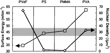
Furthermore, some groups found that the carrier mobility does not depend monotonically on the surface energy of the substrate surface.69,72,73 Yoshida et al.72 have reported that as the surface energy of the polymer modifier increased from about 35 to 47 mN m−1, the grain size of the pentacene film and carrier mobility increased, but above the surface energy of 63 mN m−1, the grain size and carrier mobility abruptly decreased (Fig. 3). They suggested that the highest field-effect mobility achieved when the surface energy of the dielectric layer was equal to the one of semiconductor layer. Similar conclusions of surface-energy-matching viewpoint have also been proposed in other works.69,73
3.2 Effect of deposition conditions
Pratontep et al.79 reported a detailed study of pentacene thin film growth by high vacuum deposition (Fig. 4). The number of pentacene islands per unit area varies significantly as the deposition rate or substrate temperature changes. When the deposition rate increased by two orders of magnitude, the number density of the islands increased by a similar factor. In contrast, the trend is reversed for the substrate temperature. The density of nucleation decreased by a few orders of magnitude as the temperature increased from 29 °C to 80 °C.
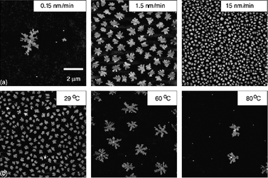 | ||
| Fig. 4 AFM surface topography (10 μm × 10 μm) of 0.5 nm-thick pentacene films grown on SiO2 substrate (a) at various deposition rates for a fixed substrate temperature of 65 °C and (b) at different substrate temperatures for a fixed deposition rate of 0.45 nm min−1. Reprinted with permission from ref. 79. Copyright 2004 Elsevier B.V. | ||
For a fixed substrate temperature, the effect of deposition rate on the growth mechanism of thin films has been extensively investigated.21,23,78,80 Bis(1,2,5-thiadiazolo)-p-quinobis(1,3-dithiole) (BTQBT)78 showed higher mobility with the increasing growth rate because the molecules laid flat on the substrate surface brought in the strongest intermolecular interaction in the stacking direction. On the other hand, for a fixed deposition rate, substrate temperature was controlled for 5,5′-bis(7-cyclohexyl-9H-fluoren-2-yl)-2,2′-bithiophene (CHFTTF).81 When the substrate temperature was raised from room temperature to 120 °C, very large, densely packed crystalline grains were formed and the average field-effect mobility increased from 8 × 10⁻³ to 0.1 cm2 V−1 s−1. At 130 °C, some cracks appeared in the crystalline grains due to the mismatch of thermal expansion coefficient between semiconductor and the substrate. Upon further increasing temperature to 150 °C, the thin film morphology changed with a significant amount of non-vertical arrangement, and the mobility decreased by one order of magnitude. Various field-effect mobility responses during different substrate deposition temperature have also been reported.74
The solvent dependence of the highly regioregular P3HT has been studied.84 It is noted that the field-effect mobility can vary significantly when different solvents are used.84 The variation is possibly due to the difference in film forming quality. Taking relatively fast drying tetrahydrofuran solvent as an example, P3HT precipitates out during solvent evaporation. A non-uniform and discontinuous P3HT film including two populations of crystals, micrometer-sized lamellar ones and nm-sized granular ones are formed. In the cases of other solvents, such as toluene or chloroform, different degrees of film discontinuity may occur depending on the solubility of the polymer and nature of the solvent.
Wang et al.85 compared three deposition methods (spin-casting, drop-casting, and dip-coating) of regioregular P3HT (RR-P3HT) film deposition using “bottom-contact” OTFT structures. Significantly higher mobility is obtained from dip-coating ultrathin films, which consist of only 2–3 monolayers. Note that the field induced carrier charges are confined to a few monolayers located at the semiconductor/insulator interface. Therefore, the relatively high carrier mobility made by dip-coating originates from the improved structural order of the semiconducting molecules near the interface. The mobility of drop-casting film is higher than that of spin-casting film, possibly because the slower evaporation rate gives time for the polymer chains to interact more strongly with each other and thus obtain a higher degree of order. The self-organization in P3HT takes place in solution processing, as the films pass from the solution phase to the solid phase. This kind of phase transformation results in a lamella structure with two-dimensional conjugated sheets.
A number of external factors can also affect the morphology of the thin film.12,86–91 For example, a correlation was observed between the solvents used for the dielectrics and the upper layer morphology.92 For polymer semiconductors, their regioregularity,12,88 molecular weight,12,87,88,93 and side-chain length91 also have substantial impact on the morphologies of their thin films. For polymers with relatively low glass transition temperatures, post-deposition annealing is the most effective method to improve thin film morphology after deposition.89,90
4. Morphology control
4.1 Surface modified with self-assembled monolayers
Since the surface properties of the substrate have significant impact on the thin film morphology and hence the performance of the transistors, intense researches are devoted to fabricating satisfactory transistors by optimizing the semiconductor/dielectric interface.50,51 By selecting appropriate methods, the undesirable interfacial effects between dielectric and semiconductor could be possibly eliminated or obviously weakened.94 Normally, the performance of the OTFTs is better when the organic film is deposited on a hydrophobic surface according to the surface “compatibility and similitude principle”.95,96 Thus, in order to improve crystalline morphology and enhance field-effect mobility, the most convenient and efficient way is to apply self-assembled monolayers (SAMs) or polymer buffers, which bind to the surface and form a dense alkyl chain forest. This kind of hydrophobic surface significantly promotes the growth of crystalline phase parallel to the surface and increases the overall coverage of the first layer. The field-effect mobility could be enhanced by the increased molecular surface mobility and reduced interactions on the surface of a hydrophobic substrate.In 1997, Lin et al.42 fabricated pentacene OTFTs on octadecyltrichlorosilane-treated silicon dioxide gate dielectric with improved field-effect mobility as high as 1.5 cm2 V−1 s−1, on/off current ratio larger than 108, near zero threshold voltage, and sub-threshold slope less than 1.6 V per decade. Subsequently, a novel and selective method to modify the alumina surfaces with the strong affinity of alkylphosphonic acid monolayers achieved a robust, extremely uniform thin film through simple spin-coating method. The exceptional value with mobility near 3 cm2 V−1 s−1 was obtained. In the previous study of our group,96 vanadyl phthalocyanine (VOPc) OTFTs with mobility up to 1.0 cm2 V−1 s−1 and on/off ratio of 106–108 were demonstrated. We found that the mobilities of devices on octadecylsilane-modified Si/SiO2 substrates was two orders of magnitude higher than that of devices on Si/SiO2 substrates. Furthermore, among these SAM-treated surfaces, we note that Forrest et al.22 reported a negative but useful effect of SAM-treated oxide, that the pentacene morphology variation was suppressed by deposition on OTS-treated gate-dielectrics, probably due to increased adhesion of pentacene to the dielectric.
Therefore, it is recognized that the excellent surface modification systems can tune the interfacial surface by varying the terminal functional group, chain length, and phase state of the molecules, which in turn affect the charge density uniformity and polarity of the surface. Reasonably optimizing these parameters could control thin film morphology and profoundly influence the final device performance.
Recently, the mechanism of the chemical composition of the gate insulator influencing crystalline phase film-growth has been investigated by several groups.72,99,100 Pentacene films deposited on SAMs of various terminal functional groups have been studied by Hu's group.101 The pentacene molecules oriented perpendicularly to the surface covered with SAMs compared with bare gold substrate, where a parallel orientation was found. The distinct morphologies were observed on these two surfaces: with apparently smaller and rod-shaped grains on clean bare Au surface but larger and island-like crystals on SAM-modified surface. Bao and coworkers62 investigated pentacene molecules deposited on dielectrics treated with different SAMs, such as hexamethyldisilazane (HMDS) and OTS. Drastically different submonolayers have been observed and ultimately influenced the mobility of 60 nm pentacene films. Faceted island morphology was found for the pentacene on HMDS surface, while dendritic island morphology on the OTS surface. The faceted island on HMDS was reminiscent of the single crystal-like morphology of pentacene. In each island, there would hardly be any internal defects during crystal packing, resulting in higher mobility. The dendritic morphology represented a divergent crystalline growth initiated from a common nucleation point. Although larger individual islands resulted in fewer intergrain boundaries, they contained far more inter- and intra-grain boundaries than the faceted islands.
Concerning polymer packing in response to surface treatment, it has been shown that the P3HT chains in the first monolayer can adopt an edge-on or a face-on arrangement depending on the surface properties of the insulator modified by the SAMs. For instance, P3HT is standing edge-on on NH2 terminated SiO2, while for alkyl chains like CH3, a face-on configuration is present.66 Therefore, the terminal groups of the SAMs appear to be crucial in determining the orientation of the P3HT molecules, which in turn strongly affects carrier mobility.
Lately, the role of crystalline, dense OTS on pentacene and C60 nucleation, thin film growth, and transistor performance has been investigated.107 By using Langmuir–Blodgett (LB) technique to vary the organization and density of the OTS monolayers systematically, different degrees of ordered OTS films were obtained. After the pentacene monolayer films were deposited under identical conditions, grazing-incidence X-ray diffraction (GIXD) and atomic force microscopy (AFM) were employed to obtain information about the morphology and crystalline order of the thin films. The pentacene GIXD spectra showed similar peaks on all the OTS surfaces indicating no clear difference in crystalline packing motifs, while AFM showed a clear trend of thin film growth mode from the more desirable 2D layer-by-layer growth on highly ordered LB films to the less favorable 3D growth on OTS vapor-treated surface. Presumably, on the more densely packed OTS layer, substrate–molecule interaction is larger since more methyl groups are able to interact with the depositing semiconductor molecules, contributing to larger first monolayer coverage. Continuous efforts to understand the effects of phase and order of the organic dielectric surface modification layer have been made by the same group.108 They developed a simple solution-deposition technique to create crystalline layers of OTS on SiO2 surfaces (Fig. 5). The high density and close packing of the terminal methyl groups in crystalline OTS monolayer interact favorably with the more desirable 2D semiconductor growth. Moreover, compared to the LB method, this technique is more amenable to large area processing. The pentacene OTFTs showed hole mobilities as high as 3.0 cm2 V−1 s−1, and electron mobilities as high as 5.3 cm2 V−1 s−1 were demonstrated for C60. As a matter of fact, it is an effective tool to finely tune the crystalline morphology and structure of the thin films by controlling the self-assembled states of the SAMs on the SiO2 substrates.

4.2 Surface modified with polymer
Polymer has been introduced as a buffer to inorganic oxide-based gate dielectrics and shown great promise for low-voltage high-performance OTFTs.91,109–112 Their interfacial compatibility with organic semiconductors makes it easy to control the chemical and physical properties of insulator surface and thus to optimize the device performance. Low surface energy and smoother topography of polymer dielectric surface contribute to the uniform in-plane crystal structure.A study based on various untreated/polymer-treated SiO2 gate dielectrics showed that pentacene films were all grown in parallel, which indicated a minor role of surface chemical characteristics in pentacene thin film transistor response.41 Recently, the side group orientation of polymer used as the modified layer has been noticed. Wang et al.91 changed the tilt angle of polystyrene phenyl groups and the corresponding surface energy of films by thermal annealing. A flatter orientation of phenyl ring produced by higher temperature thermal treatments optimized the surface energy of polystyrene film, resulting in higher crystallinity of pentacene films deposited onto it and an improved interconnection between the crystalline domains. The mobility reached as high as 4 cm2 V−1 s−1 in the saturation region.
However, large discrepancies in performance, even with apparently identical surface treatments, indicate that additional surface parameters must be identified and controlled in order to optimize OTFTs. Recently, the intriguing question is how polymer dielectric chain segmental dynamics influences the growth orientation of organic semiconductors and corresponding OTFTs performance.113–116
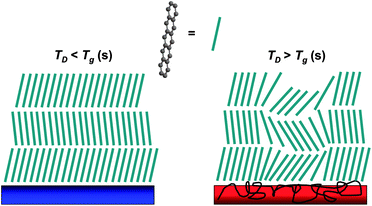
In contrast to higher substrate temperature engendering larger grain size and enhancing subsequent interconnection, Kim et al.114 found that the grain size of pentacene, deposited on polymers with lower glass transition temperatures, exhibited a dramatic decrease of mobility with the increase of substrate temperature. General and abrupt mobility transitions occurred at well-defined pentacene film growth temperatures indicating the characteristics of each underlying polymer dielectric. The authors attributed this kind of decrease to the effect of polymer dielectric chain mobility on overlying organic semiconductor thin film growth. Subsequently, a continued investigation and detailed discussion have been reported by the same group (Fig. 6).115,116 They proposed a potential mechanism that, above a critical temperature, a significant perturbation of the rubbery phase polymer surface occured, resulting in a rougher dielectric/semiconductor interface. The rougher gate dielectric surface afforded smaller grain sizes, collapse of the thin film structures, decreased semiconductor film texturing, and reduced OTFTs performance.
 | ||
| Fig. 6 Schematic diagram of pentacene film microstructural variation on polymer gate dielectrics at different substrate temperature. Reprinted with permission from ref. 115. Copyright 2009 The American Chemical Society. | ||
In a similar approach, Duan et al.117 vapor deposited copper phthalocyanine (CuPc) on polycaprolactone (PCL)- and poly(ethylene oxide) PEO-treated dielectric at different substrate temperature (Td). Interestingly, unlike the mobility of SiO2-OTFTs which slightly changes with increasing temperature, the mobility of PCL-OTFTs increases much more sharply when Td is well above the melting point of the treated polymer. The incongruence in these results possibly stems from the conjugated CuPc molecules used in this study, which can effectively assemble under the assistance of the movement of polymer chains.
It is noteworthy that, in spite of different results reported, polymer chain dynamics play an important role on the performance of OTFTs. Controlling chain movement can achieve optimum film morphologies and maximum OTFTs performance, and also contribute to the more rational fabrication of advanced organic electronics.
4.3 Techniques for molecular alignment
The application of alignment to conjugated molecules offers a unique approach for constructing high performance organic semiconductor devices. The alignment enables better orbital overlap in which the π–π stacking direction is arranged in the same direction as that of the current flow. Therefore, maximising charge carrier mobility can be simplified to controlling the chain packing orientation and enforcing intermolecular orbital overlap which are mainly responsible for effective charge transfer, especially for polymeric semiconductors. To achieve ordering orientation of organic semiconductors, various novel fabrication techniques have been developed to align the molecular backbones, such as directly stretching or rubbing the thin films,118–120 depositing organic semiconductors on alignment layers,121,122 epitaxial growth of organic semiconductors,123,124 LB technique,125–129 or zone casting technique, and so forth.Mechanical stretching or rubbing the semiconductor films is an efficient way to align conjugated molecules. A study based on poly(3-octylthiophene) (P3OT) films was reported.130 The P3OT films were spin-coated on polyethylene foil and subsequently oriented by stretching the film together with the foil. The relationship between the stretching ratio and the mobility anisotropy was observed. When the film was stretched 4.5 times longer, a mobility anisotropy of 4.5 was obtained. However, the mobilities were relatively low, and no major change of the absolute value of mobility was observed.
In 1991, Wittmann and Smith initially proposed the highly oriented poly(tetrafluoroethylene) (PTFE) film prepared by the friction transfer technique.131 They demonstrated the possibility of orienting various organic systems including polymers and conjugated molecules onto ultrathin crystalline PTFE films. To date, a wide variety of materials were successfully oriented on this substrate.122,132–134 Recently, Dong et al.122 have extended this facile method for the fabrication of oriented rigid rod conjugated polymer films (Fig. 7). When poly(para-phenylene ethynylene)s with thioacetyl end (TA-PPE) solution was drop-casted on friction-transferred PTFE substrate, they formed highly ordering TA-PPE films with their conjugated backbones parallel to the PTFE sliding direction.
 | ||
| Fig. 7 Schematic diagram of sliding a PTFE rod at constant pressure against the substrates held at approximately 280 °C for obtaining an aligned PTFE layer, and then TA-PPE films were obtained by drop-casting TA-PPE tetrahydrofuran solution onto the oriented PTFE layer. (a) Polarized optical micrograph of aligned TA-PPE films on oriented PTFE of glass substrates under the 45° of polarizer with respect to the sliding direction, (b) SEM image of the aligned films. Reprinted with permission from ref. 122. Copyright 2008 The American Chemical Society. | ||
The liquid-crystalline (LC) semiconductors are more vulnerable to the surface state. Sirringhaus et al.52,121 reported the alignment of LC molecules on rubbed substrate. The liquid-crystalline polymer, poly(9,9-dioctylfluorene-co-bithiophene) (F8T2), was deposited onto a mechanically rubbed polyimide alignment layer. At temperatures above 265 °C, the F8T2 chains aligned in parallel to the rubbing direction of underlying layer. After quenching to room temperature, the alignment of the polymer chains is preserved but crystallization is suppressed. Values for the anisotropy of the field-effect mobility are 5–8 varying between devices parallel or perpendicular to the alignment direction, implying charge transport along the conjugated segments of the polymer backbone is faster than interchain hopping between adjacent chains.
An elegant epitaxial growth technology was also used to fabricate organic films, as used in the inorganic semiconductor industry. Heteroepitaxy is of great potential in controlling molecular ordering of organic semiconductors and fabricating highly ordered and aligned structures for organic electronics.24,123,134 Unfortunately, for organic molecules, owing to the strong interaction between the molecules and the substrate, molecules tend to adhere flat to the substrate, leading to low in-plane mobility. To overcome this problem, a weak epitaxy growth (WEG) technique was developed to fabricate large and highly oriented domains, in which the molecules were epitaxial and upright on the substrate. The organic electronic devices with such highly oriented and continuous films serving as active layers exhibited very high charge carrier mobilities, close to those of the single-crystal devices. However, attention must be paid to the new problem introduced by this approach. For instance, Wang et al.124 used a semiconductor molecule like para-hexaphenyle (p-6P) as the template to induce the crystallization of zinc phalocyanine (ZnPc) in thin film transistors. However, the mobilities were mainly attributed to p-6P but not ZnPc because p-6P formed the most part of the active channel between organic semiconductors and dielectric. Recently, Li et al.135 reported a new strategy of using an easily crystallized insulating molecule as the template layer to induce the crystallization of organic semiconductors. When flat thin layers of 6,13-pentacenequinone (PQ) were employed, the vacuum-deposited rubrene thin films yield transistors with good field effect mobilities. Particularly interesting is the crystallization of rubrene started on the flat PQ domains which only covered part of the substrate surface, and then extends to the areas that were not covered. Therefore, in this case, the authors suggested that rubrene films were responsible for charge transport and current modulation.
Small molecules and conjugated polymer semiconductors can also be aligned through the LB technique.126,128,129 By applying a lateral pressure to the monolayer film at the air–water interface, the ultrathin film with a high degree of order and precision in thickness can be obtained. The first LB film transistor was fabricated in the early 1990s.127,136 Later, Xu et al.126 reported the P3HT LB monolayer films with mobilities as high as 2 × 10⁻² cm2 V−1 s−1. Recently, the LB technique was also used to deposit the active organic semiconductor layer-by-layer to identify the role of the monolayer in the organic transistors.137 The results indicated that, compared to the LB monolayer, the crystallinity of the semiconductor films decreased and the molecular ordering reduced in the multilayer LB layer.
Compared to traditional solution-processing techniques, such as dropping, dipping and casting, the zone-casting technique offers an advantage of fabricating long-range-oriented organic semiconductors (Fig. 8).138–140 Here, a continuously supplied solution is spread by means of a nozzle onto a moving support under the appropriate rate of solvent evaporation. The alignment of hexa-peri-hexabenzocoronene (HBC) derivatives was fabricated where long range ordered columnar structures were achieved.138 The successful application clearly highlights the effectiveness of this technique in obtaining directionally arranged supramolecular structures. However, local intracolumnar packing defects were observed sporadically, which may disturb charge carrier transport.
 | ||
| Fig. 8 (a) Chemical structure of dodecyl-substituted HBC derivative (HBC-C12); (b) schematic presentation of the zone-casting technique; (c) an optical microscopy image taken in reflection mode for a zone-cast HBC-C12 layer on a silicon substrate; (d) large-area image from HRTEM of a zone-cast HBC-C12 layer displaying the homogeneous film formation with single columnar features lying in the zone-casting direction. Reprinted with permission from ref. 124. Copyright 2007 Wiley–VCH. | ||
5. Conclusions
In summary, we have reviewed theoretical and experimental works exploring the influence of growth parameters on the structure and morphology of semiconductor thin films, in particular, making further efforts to optimize these factors for the fabrication of high-performance OTFTs. Correlations between thin film morphology and surface characteristics have been established. Surface modification as a technique can efficiently change the structure of the thin film. The formation of large single-crystal domains and the high degree of molecular ordering are desired with the high mobilities obtained from these devices. Furthermore, the morphology can be manipulated by varying the deposition rate, substrate temperature, or the solvent used. Novel optimized methods to achieve desirable field-effect mobility have also been presented. With a better understanding of morphology dominated factors, further enhancement and explorations in high quality films by improving molecules packing is expected. The substrate and processing options open new opportunities for excellent device performance.Acknowledgements
The authors acknowledge the financial support from National Natural Science Foundation of China (20872146 and 50725311), Ministry of Science and Technology of China and Chinese Academy of Sciences.Notes and references
- C. D. Dimitrakopoulos and P. R. L. Malenfant, Adv. Mater., 2002, 14, 99 CrossRef CAS.
- J. Fraxedas, Adv. Mater., 2002, 14, 1603 CrossRef CAS.
- G. Horowitz, Adv. Mater., 1998, 10, 365 CrossRef CAS.
- T. W. Kelley, P. F. Baude, C. Gerlach, D. E. Ender, D. Muyres, M. A. Haase, D. E. Vogel and S. D. Theiss, Chem. Mater., 2004, 16, 4413 CrossRef CAS.
- C. R. Newman, C. D. Frisbie, D. A. da Silva, J. L. Bredas, P. C. Ewbank and K. R. Mann, Chem. Mater., 2004, 16, 4436 CrossRef CAS.
- G. Horowitz, J. Mater. Res., 2004, 19, 1946 CAS.
- M. Muccini, Nat. Mater., 2006, 5, 605 CrossRef CAS.
- T. B. Singh and N. S. Sariciftci, Annu. Rev. Mater. Res., 2006, 36, 199 CrossRef CAS.
- D. Braga and G. Horowitz, Adv. Mater., 2009, 21, 1473 CrossRef CAS.
- H. Sirringhaus, N. Tessler and R. H. Friend, Science, 1998, 280, 1741 CrossRef CAS.
- L. Q. Li, Q. X. Tang, H. X. Li, X. D. Yang, W. P. Hu, Y. B. Song, Z. G. Shuai, W. Xu, Y. Q. Liu and D. B. Zhu, Adv. Mater., 2007, 19, 2613 CrossRef CAS.
- H. Sirringhaus, P. J. Brown, R. H. Friend, M. M. Nielsen, K. Bechgaard, B. M. W. Langeveld-Voss, A. J. H. Spiering, R. A. J. Janssen, E. W. Meijer, P. Herwig and D. M. de Leeuw, Nature, 1999, 401, 685 CrossRef CAS.
- D. M. DeLongchamp, S. Sambasivan, D. A. Fischer, E. K. Lin, P. Chang, A. R. Murphy, J. M. J. Frechet and V. Subramanian, Adv. Mater., 2005, 17, 2340 CrossRef CAS.
- H. E. Katz and J. Huang, Annu. Rev. Mater. Res., 2009, 39, 71 CrossRef CAS.
- H. N. Tsao and K. Mullen, Chem. Soc. Rev., 2010, 39, 2372 RSC.
- L. Jiang, W. P. Hu, Z. M. Wei, W. Xu and H. Meng, Adv. Mater., 2009, 21, 3649 CrossRef CAS.
- L. Jiang, H. L. Dong and W. P. Hu, J. Mater. Chem., 2010, 20, 4994 RSC.
- C. Reese and Z. N. Bao, Mater. Today, 2007, 10, 20 CrossRef CAS.
- R. W. I. de Boer, M. E. Gershenson, A. F. Morpurgo and V. Podzorov, Phys. Status Solidi A, 2004, 201, 1302 CrossRef CAS.
- R. A. Street, Adv. Mater., 2009, 21, 2007 CrossRef CAS.
- F. Heringdorf, M. C. Reuter and R. M. Tromp, Appl. Phys. A: Mater. Sci. Process., 2004, 78, 787 CrossRef CAS.
- S. R. Forrest, Chem. Rev., 1997, 97, 1793 CrossRef CAS.
- R. Ruiz, D. Choudhary, B. Nickel, T. Toccoli, K. C. Chang, A. C. Mayer, P. Clancy, J. M. Blakely, R. L. Headrick, S. Iannotta and G. G. Malliaras, Chem. Mater., 2004, 16, 4497 CrossRef CAS.
- F. Heringdorf, M. C. Reuter and R. M. Tromp, Nature, 2001, 412, 517 CrossRef CAS.
- S. Y. Yang, K. Shin and C. E. Park, Adv. Funct. Mater., 2005, 15, 1806 CrossRef CAS.
- H. S. Lee, D. H. Kim, J. H. Cho, Y. D. Park, J. S. Kim and K. Cho, Adv. Funct. Mater., 2006, 16, 1859 CrossRef CAS.
- M. M. Ling and Z. N. Bao, Chem. Mater., 2004, 16, 4824 CrossRef CAS.
- A. Tsumura, H. Koezuka and T. Ando, Appl. Phys. Lett., 1986, 49, 1210 CrossRef CAS.
- G. Horowitz, D. Fichou, X. Z. Peng, Z. G. Xu and F. Garnier, Solid State Commun., 1989, 72, 381 CrossRef CAS.
- R. Ruiz, A. Papadimitratos, A. C. Mayer and G. G. Malliaras, Adv. Mater., 2005, 17, 1795 CrossRef CAS.
- J. Locklin, M. E. Roberts, S. C. B. Mannsfeld and Z. N. Bao, Polym. Rev., 2006, 46, 79 Search PubMed.
- S. Verlaak, S. Steudel, P. Heremans, D. Janssen and M. S. Deleuze, Phys. Rev. B: Condens. Matter Mater. Phys., 2003, 68, 195409 CrossRef.
- A. C. Mayer, A. Kazimirov and G. G. Malliaras, Phys. Rev. Lett., 2006, 97, 105503 CrossRef.
- L. F. Drummy and D. C. Martin, Adv. Mater., 2005, 17, 903 CrossRef CAS.
- D. Knipp, R. A. Street, A. Volkel and J. Ho, J. Appl. Phys., 2003, 93, 347 CrossRef CAS.
- S. H. Kim, M. Jang, H. Yang and C. E. Park, J. Mater. Chem., 2010, 20, 5612 RSC.
- G. C. Yuan, Z. S. Lu, Z. Xu, C. Gong, Q. L. Song, S. L. Zhao, F. J. Zhang, N. Xu, Y. Gan, H. B. Yang and C. M. Li, Org. Electron., 2009, 10, 1388 CrossRef CAS.
- C. D. Dimitrakopoulos, A. R. Brown and A. Pomp, J. Appl. Phys., 1996, 80, 2501 CrossRef CAS.
- H. Yanagisawa, T. Tamaki, M. Nakamura and K. Kudo, Thin Solid Films, 2004, 464, 398 CrossRef.
- G. Horowitz and M. E. Hajlaoui, Adv. Mater., 2000, 12, 1046 CrossRef CAS.
- H. L. Cheng, Y. S. Mai, W. Y. Chou and L. R. Chang, Appl. Phys. Lett., 2007, 90, 171926 CrossRef.
- Y. Y. Lin, D. J. Gundlach, S. F. Nelson and T. N. Jackson, IEEE Electron Device Lett., 1997, 18, 606 CrossRef CAS.
- A. Bolognesi, M. Berliocchi, M. Manenti, A. Di Carlo, P. Lugli, K. Lmimouni and C. Dufour, IEEE Trans. Electron Devices, 2004, 51, 1997 CrossRef CAS.
- S. Pratontep, F. Nuesch, L. Zuppiroli and M. Brinkmann, Phys. Rev. B: Condens. Matter Mater. Phys., 2005, 72, 085211 CrossRef.
- G. Horowitz, M. E. Hajlaoui and R. Hajlaoui, J. Appl. Phys., 2000, 87, 4456 CrossRef CAS.
- M. Mottaghi and G. Horowitz, Org. Electron., 2006, 7, 528 CrossRef CAS.
- R. Matsubara, N. Ohashi, M. Sakai, K. Kudo and M. Nakamura, Appl. Phys. Lett., 2008, 92, 242108 CrossRef.
- J. Rivnay, L. H. Jimison, J. E. Northrup, M. F. Toney, R. Noriega, S. F. Lu, T. J. Marks, A. Facchetti and A. Salleo, Nat. Mater., 2009, 8, 952 CrossRef CAS.
- M. H. Choo, J. H. Kim and S. Im, Appl. Phys. Lett., 2002, 81, 4640 CrossRef CAS.
- C.-a. Di, Y. Liu, G. Yu and D. Zhu, Acc. Chem. Res., 2009, 42, 1573 CrossRef CAS.
- H. Ma, H. L. Yip, F. Huang and A. K. Y. Jen, Adv. Funct. Mater., 2010, 20, 1371 CrossRef CAS.
- A. Salleo, M. L. Chabinyc, M. S. Yang and R. A. Street, Appl. Phys. Lett., 2002, 81, 4383 CrossRef CAS.
- X. N. Sun, C. A. Di and Y. Q. Liu, J. Mater. Chem., 2010, 20, 2599 RSC.
- Y. D. Park, J. A. Lim, H. S. Lee and K. Cho, Mater. Today, 2007, 10, 46 CAS.
- S. E. Fritz, T. W. Kelley and C. D. Frisbie, J. Phys. Chem. B, 2005, 109, 10574 CrossRef CAS.
- M. L. Chabinyc, R. Lujan, F. Endicott, M. F. Toney, I. McCulloch and M. Heeney, Appl. Phys. Lett., 2007, 90, 233508 CrossRef.
- P. S. Jo, J. Sung, C. Park, E. Kim, D. Y. Ryu, S. Pyo, H. C. Kim and J. M. Hong, Adv. Funct. Mater., 2008, 18, 1202 CrossRef CAS.
- Y. Jung, R. J. Kline, D. A. Fischer, E. K. Lin, M. Heeney, I. McCulloch and D. M. DeLongchamp, Adv. Funct. Mater., 2008, 18, 742 CrossRef CAS.
- K. Suemori, S. Uemura, M. Yoshida, S. Hoshino, N. Takada, T. Kodzasa and T. Kamata, Appl. Phys. Lett., 2008, 93, 033308 CrossRef.
- D. Knipp, R. A. Street and A. R. Volkel, Appl. Phys. Lett., 2003, 82, 3907 CrossRef CAS.
- D. Knipp, R. A. Street, B. Krusor, R. Apte and J. Ho, J. Non-Cryst. Solids, 2002, 299, 1042 CrossRef.
- H. C. Yang, T. J. Shin, M. M. Ling, K. Cho, C. Y. Ryu and Z. N. Bao, J. Am. Chem. Soc., 2005, 127, 11542 CrossRef CAS.
- S. Steudel, S. De Vusser, S. De Jonge, D. Janssen, S. Verlaak, J. Genoe and P. Heremans, Appl. Phys. Lett., 2004, 85, 4400 CrossRef CAS.
- K. Shin, C. W. Yang, S. Y. Yang, H. Y. Jeon and C. E. Park, Appl. Phys. Lett., 2006, 88, 072109 CrossRef.
- L. L. Chua, P. K. H. Ho, H. Sirringhaus and R. H. Friend, Adv. Mater., 2004, 16, 1609 CrossRef CAS.
- D. H. Kim, Y. D. Park, Y. S. Jang, H. C. Yang, Y. H. Kim, J. I. Han, D. G. Moon, S. J. Park, T. Y. Chang, C. W. Chang, M. K. Joo, C. Y. Ryu and K. W. Cho, Adv. Funct. Mater., 2005, 15, 77 CrossRef CAS.
- T. Umeda, D. Kumaki and S. Tokito, J. Appl. Phys., 2009, 105, 024516 CrossRef.
- J. Gao, K. Asadi, J. B. Xu and J. An, Appl. Phys. Lett., 2009, 94, 093302 CrossRef.
- W. Y. Chou, C. W. Kuo, H. L. Cheng, Y. R. Chen, F. C. Tang, F. Y. Yang, D. Y. Shu and C. C. Liao, Appl. Phys. Lett., 2006, 89, 112126 CrossRef.
- P. Miskiewicz, S. Kotarba, J. Jung, T. Marszalek, M. Mas-Torrent, E. Gomar-Nadal, D. B. Amabilino, C. Rovira, J. Veciana, W. Maniukiewicz and J. Ulanski, J. Appl. Phys., 2008, 104, 054509 CrossRef.
- J. Takeya, T. Nishikawa, T. Takenobu, S. Kobayashi, Y. Iwasa, T. Mitani, C. Goldmann, C. Krellner and B. Batlogg, Appl. Phys. Lett., 2004, 85, 5078 CrossRef CAS.
- M. Yoshida, S. Uemura, T. Kodzasa, T. Kamata, M. Matsuzawa and T. Kawai, Synth. Met., 2003, 137, 967 CrossRef CAS.
- M. Mezger, H. Reichert, S. Schoder, J. Okasinski, H. Schroder, H. Dosch, D. Palms, J. Ralston and V. Honkimaki, Proc. Natl. Acad. Sci. U. S. A., 2006, 103, 18401 CrossRef CAS.
- B. A. Jones, A. Facchetti, M. R. Wasielewski and T. J. Marks, Adv. Funct. Mater., 2008, 18, 1329 CrossRef CAS.
- A. Facchetti, J. Letizia, M. H. Yoon, M. Mushrush, H. E. Katz and T. J. Marks, Chem. Mater., 2004, 16, 4715 CrossRef CAS.
- J. G. Laquindanum, H. E. Katz, A. J. Lovinger and A. Dodabalapur, Chem. Mater., 1996, 8, 2542 CrossRef CAS.
- Z. N. Bao, A. J. Lovinger and A. Dodabalapur, Adv. Mater., 1997, 9, 42 CAS.
- J. G. Xue and S. R. Forrest, Appl. Phys. Lett., 2001, 79, 3714 CrossRef CAS.
- S. Pratontep, M. Brinkmann, F. Nuesch and L. Zuppiroli, Synth. Met., 2004, 146, 387 CrossRef CAS.
- S. Pratontep, M. Brinkmann, F. Nuesch and L. Zuppiroli, Phys. Rev. B: Condens. Matter Mater. Phys., 2004, 69, 165201 CrossRef.
- J. Locklin, D. W. Li, S. C. B. Mannsfeld, E. J. Borkent, H. Meng, R. Advincula and Z. Bao, Chem. Mater., 2005, 17, 3366 CrossRef CAS.
- G. H. Lu, L. G. Li and X. N. Yang, Adv. Mater., 2007, 19, 3594 CrossRef CAS.
- Z. Bao, A. Dodabalapur and A. J. Lovinger, Appl. Phys. Lett., 1996, 69, 4108 CrossRef CAS.
- A. R. Brown, D. M. Deleeuw, E. E. Havinga and A. Pomp, Synth. Met., 1994, 68, 65 CrossRef CAS.
- G. M. Wang, J. Swensen, D. Moses and A. J. Heeger, J. Appl. Phys., 2003, 93, 6137 CrossRef CAS.
- O. D. Jurchescu, J. Baas and T. T. M. Palstra, Appl. Phys. Lett., 2004, 84, 3061 CrossRef CAS.
- A. Zen, M. Saphiannikova, D. Neher, J. Grenzer, S. Grigorian, U. Pietsch, U. Asawapirom, S. Janietz, U. Scherf, I. Lieberwirth and G. Wegner, Macromolecules, 2006, 39, 2162 CrossRef CAS.
- R. J. Kline, M. D. McGehee, E. N. Kadnikova, J. S. Liu, J. M. J. Frechet and M. F. Toney, Macromolecules, 2005, 38, 3312 CrossRef CAS.
- Q. L. Bao, J. Li, C. M. Li, Z. L. Dong, Z. S. Lu, F. Qin, C. Gong and J. Guo, J. Phys. Chem. B, 2008, 112, 12270 CrossRef CAS.
- M. C. Kwan, K. H. Cheng, P. T. Lai and C. M. Che, Solid-State Electron., 2007, 51, 77 CrossRef CAS.
- Y. Wang, O. Acton, G. Ting, T. Weidner, P. J. Shamberge, H. Ma, F. S. Ohuchi, D. G. Castner and A. K. Y. Jen, Org. Electron., 2010, 11, 1066 CrossRef CAS.
- R. Parashkov, E. Becker, G. Ginev, T. Riedl, H. H. Johannes and W. Kowalsky, J. Appl. Phys., 2004, 95, 1594 CrossRef CAS.
- H. N. Tsao, D. Cho, J. W. Andreasen, A. Rouhanipour, D. W. Breiby, W. Pisula and K. Mullen, Adv. Mater., 2009, 21, 209 CrossRef CAS.
- F. C. Chen and C. H. Liao, Appl. Phys. Lett., 2008, 93, 103310 CrossRef.
- P. Fontaine, D. Goguenheim, D. Deresmes, D. Vuillaume, M. Garet and F. Rondelez, Appl. Phys. Lett., 1993, 62, 2256 CrossRef CAS.
- L. Q. Li, Q. X. Tang, H. X. Li and W. P. Hu, J. Phys. Chem. B, 2008, 112, 10405 CrossRef CAS.
- P. Dhagat, H. M. Haverinen, R. J. Kline, Y. Jung, D. A. Fischer, D. M. DeLongchamp and G. E. Jabbour, Adv. Funct. Mater., 2009, 19, 2365 CrossRef CAS.
- A. Facchetti, M. H. Yoon and T. J. Marks, Adv. Mater., 2005, 17, 1705 CrossRef CAS.
- Y. Jang, J. H. Cho, D. H. Kim, Y. D. Park, M. Hwang and K. Cho, Appl. Phys. Lett., 2007, 90, 132104 CrossRef.
- I. Yagi, K. Tsukagoshi and Y. Aoyagi, Appl. Phys. Lett., 2005, 86, 103503 CrossRef.
- W. S. Hu, Y. T. Tao, Y. J. Hsu, D. H. Wei and Y. S. Wu, Langmuir, 2005, 21, 2260 CrossRef CAS.
- T. W. Kelley, L. D. Boardman, T. D. Dunbar, D. V. Muyres, M. J. Pellerite and T. Y. P. Smith, J. Phys. Chem. B, 2003, 107, 5877 CrossRef CAS.
- I. G. Hill, C. M. Weinert, L. Kreplak and B. P. van Zyl, Appl. Phys. A: Mater. Sci. Process., 2009, 95, 81 CrossRef CAS.
- D. H. Kim, H. S. Lee, H. C. Yang, L. Yang and K. Cho, Adv. Funct. Mater., 2008, 18, 1363 CrossRef CAS.
- J. Aizenberg, A. J. Black and G. M. Whitesides, Nature, 1999, 398, 495 CrossRef CAS.
- H. S. Lee, D. H. Kim, J. H. Cho, M. Hwang, Y. Jang and K. Cho, J. Am. Chem. Soc., 2008, 130, 10556 CrossRef CAS.
- A. Virkar, S. Mannsfeld, J. H. Oh, M. F. Toney, Y. H. Tan, G. Y. Liu, J. C. Scott, R. Miller and Z. Bao, Adv. Funct. Mater., 2009, 19, 1962 CrossRef CAS.
- Y. Ito, A. A. Virkar, S. Mannsfeld, J. H. Oh, M. Toney, J. Locklin and Z. A. Bao, J. Am. Chem. Soc., 2009, 131, 9396 CrossRef CAS.
- Y. L. Wu, P. Liu and B. S. Ong, Appl. Phys. Lett., 2006, 89, 013505 CrossRef.
- X. H. Zhang, B. Domercq and B. Kippelen, Appl. Phys. Lett., 2007, 91, 092114 CrossRef.
- M. H. Yoon, C. Kim, A. Facchetti and T. J. Marks, J. Am. Chem. Soc., 2006, 128, 12851 CrossRef CAS.
- L. Zhang, C.-a. Di, Y. Zhao, Y. Guo, X. Sun, Y. Wen, W. Zhou, X. Zhan, G. Yu and G. Y. Liu, Adv. Mater., 2010, 22, 3537 CrossRef CAS.
- C. Kim, J. R. Quinn, A. Facchetti and T. J. Marks, Adv. Mater., 2009, 22, 342.
- C. Kim, A. Facchetti and T. J. Marks, Adv. Mater., 2007, 19, 2561 CrossRef CAS.
- C. Kim, A. Facchetti and T. J. Marks, J. Am. Chem. Soc., 2009, 131, 9122 CrossRef CAS.
- C. Kim, A. Facchetti and T. J. Marks, Science, 2007, 318, 76 CrossRef CAS.
- X. L. Duan, Q. X. Tang, J. Qiu, Y. H. Niu, Z. G. Wang and W. P. Hu, Appl. Phys. Lett., 2009, 95, 113301 CrossRef.
- S. J. Kang, Y. Y. Noh, K. J. Baeg, J. Ghim, J. H. Park, D. Y. Kim, J. S. Kim, J. H. Park and K. Cho, Appl. Phys. Lett., 2008, 92, 052017.
- M. L. Swiggers, G. Xia, J. D. Slinker, A. A. Gorodetsky, G. G. Malliaras, R. L. Headrick, B. T. Weslowski, R. N. Shashidhar and C. S. Dulcey, Appl. Phys. Lett., 2001, 79, 1300 CrossRef CAS.
- X. L. Chen, A. J. Lovinger, Z. N. Bao and J. Sapjeta, Chem. Mater., 2001, 13, 1341 CrossRef CAS.
- H. Sirringhaus, R. J. Wilson, R. H. Friend, M. Inbasekaran, W. Wu, E. P. Woo, M. Grell and D. D. C. Bradley, Appl. Phys. Lett., 2000, 77, 406 CrossRef CAS.
- H. L. Dong, H. X. Li, E. J. Wang, Z. M. Wei, W. Xu, W. P. Hu and S. K. Yan, Langmuir, 2008, 24, 13241 CrossRef CAS.
- J. L. Yang and D. H. Yan, Chem. Soc. Rev., 2009, 38, 2634 RSC.
- H. B. Wang, F. Zhu, J. L. Yang, Y. H. Geng and D. H. Yan, Adv. Mater., 2007, 19, 2168 CrossRef CAS.
- G. Wegner, Thin Solid Films, 1992, 216, 105 CrossRef CAS.
- G. F. Xu, Z. A. Bao and J. T. Groves, Langmuir, 2000, 16, 1834 CrossRef CAS.
- J. Paloheimo, P. Kuivalainen, H. Stubb, E. Vuorimaa and P. Ylilahti, Appl. Phys. Lett., 1990, 56, 1157 CrossRef CAS.
- R. Singhal, A. Chaubey, K. Kaneto, W. Takashima and B. D. Malhotra, Biotechnol. Bioeng., 2004, 85, 277 CrossRef CAS.
- J. Matsui, Y. Sato, T. Mikayama and T. Miyashita, Langmuir, 2007, 23, 8602 CrossRef CAS.
- G. Gustafsson, O. Inganas and S. Stafstrom, Solid State Commun., 1990, 76, 203 CrossRef.
- J. C. Wittmann and P. Smith, Nature, 1991, 352, 414 CrossRef CAS.
- K. R. Amundson, B. J. Sapjeta, A. J. Lovinger and Z. N. Bao, Thin Solid Films, 2002, 414, 143 CrossRef CAS.
- M. Brinkmann, J. C. Wittmann, M. Barthel, M. Hanack and C. Chaumont, Chem. Mater., 2002, 14, 904 CrossRef CAS.
- P. Damman, M. Dosiere and J. C. Wittmann, Macromolecules, 1997, 30, 8386 CrossRef CAS.
- Z. F. Li, J. Du, Q. Tang, F. Wang, J. B. Xu, J. C. Yu and Q. A. Miao, Adv. Mater., 2010, 22, 3242 CrossRef CAS.
- J. Paloheimo, H. Stubb, P. Ylilahti, P. Dyreklev and O. Inganas, Thin Solid Films, 1992, 210, 283 CrossRef.
- Z. M. Wei, W. Xu, W. P. Hu and D. B. Zhu, Langmuir, 2009, 25, 3349 CrossRef CAS.
- W. Pisula, A. Menon, M. Stepputat, I. Lieberwirth, U. Kolb, A. Tracz, H. Sirringhaus, T. Pakula and K. Mullen, Adv. Mater., 2005, 17, 684 CrossRef CAS.
- P. Miskiewicz, M. Mas-Torrent, J. Jung, S. Kotarba, I. Glowacki, E. Gomar-Nadal, D. B. Amabilino, J. Veciana, B. Krause, D. Carbone, C. Rovira and J. Ulanski, Chem. Mater., 2006, 18, 4724 CrossRef CAS.
- A. Tracz, J. K. Jeszka, M. D. Watson, W. Pisula, K. Mullen and T. Pakula, J. Am. Chem. Soc., 2003, 125, 1682 CrossRef CAS.
| This journal is © The Royal Society of Chemistry 2011 |