Ultrasensitive water-processed monolayer photodetectors†
Song
Liu
a,
Zhongming
Wei
b,
Yang
Cao
a,
Lin
Gan
a,
Zhenxing
Wang
a,
Wei
Xu
b,
Xuefeng
Guo
*a and
Daoben
Zhu
b
aBeijing National Laboratory for Molecular Sciences (BNLMS), State Key Laboratory for Structural Chemistry of Unstable and Stable Species, College of Chemistry and Molecular Engineering, Peking University, Beijing, 100871, P. R. China. E-mail: guoxf@pku.edu.cn; Tel: (+86) 10-62757789
bKey Laboratory of Organic Solids, Beijing National Laboratory for Molecular Sciences (BNLMS), Institute of Chemistry, Chinese Academy of Sciences, Beijing, 100190, P. R. China
First published on 1st February 2011
Abstract
Solution-processed photodetectors with high sensitivity over a broad spectral range are highly desirable for low-cost, large-area sensing applications in both industrial and scientific communities. In general, the detector sensitivities are limited by inefficient carrier dissociation and transport of materials and high contact Schottky barriers. Here we detail a combined method to make ultrasensitive water-processed photodetectors based on high-performance Langmuir–Blodgett (LB) monolayer transistors of semiconducting copper phthalocyanine (CuPc), using quasi one-dimensional (1D) ballistically-conductive single-walled carbon nanotubes (SWNTs) as point contacts. Operating at low biases, the monolayer photodetectors exhibit responsivities greater than 108 A W−1, detectivities greater than 7 × 10¹⁵ Jones, and high reproducibility. These results form the basis for new types of high-performance photodetectors for a variety of possible sensor applications.
Introduction
A growing research interest in the field of optoelectronic devices is the development of solution-processed photodetectors with high sensitivity over the broad spectral range for low-cost, large-area sensing applications in both industrial and scientific communities, for example, environmental monitoring, remote control, telecommunication, day- and night-time surveillance, and chemical/biological imaging.1–5 In light of the spectral needs in the separate applications, much research on inorganic materials, including InP,6ZnO,7GaN,8Si,9 and InGaAs,10,11 has been conducted to develop different photodetectors that can sense from the ultraviolet (UV)-visible to the infrared. The calculated photoresponsivities of these devices were generally less than 10 A W−1. The typical detectivities of InGaAs and silicon photodetectors are moderate, ∼ 1012 Jones (1 Jones = 1 cm Hz1/2/W). To achieve high near-infrared sensitivity, colloidal inorganic semiconductor quantum dots (PdS) were used to fabricate two-terminal photodetectors with gold interdigitated electrodes.12–14 However, by using the “in-plane” device structure with an electrode spacing >5μm, the driving voltage is too high (>40V) to be used with any commercially available thin film transistors. Therefore, rational fabrication of solution-cast photodetectors, which can be operated with high sensitivity, low-power consumption, low dark current, and high yield over a broad spectral range at room temperature, boosts development. Among solution-cast photodetectors, water-processed devices might be the priority because of their environmental friendliness.Organic semiconducting materials are attractive alternatives because of the ease of solution processing and the tunable optical and electronic properties arising from their flexible molecular structure engineering.15 Semiconducting polymers16–20 and organic/nanocrystal composites21–24 have been demonstrated to fabricate low-cost photodetectors through simple coating techniques with a spectral response in the visible range. To manufacture efficient photodetectors in the spectral region above 1 μm, several polymers with low bandgaps were designed to develop infrared photodetectors.5,25–27 However, the device performance is still poor (the measured responsivities ≤0.2 A W−1) due to a combination of several loss mechanisms: low carrier mobility due to long-range molecular disordering, inefficient carrier injection/extraction due to high contact Schottky barriers, and inefficient dissociation of photogenerated excitons causing substantial charge recombination. An alternative approach for achieving high sensitivity by improving efficient carrier transport in organic semiconductors is therefore highly desirable at this time.
Here we report such an approach, by which a new class of ultrasensitive solution (water)-processed photodetectors in the visible region based on high-performance photoresponsive organic field-effect transistors (OFETs) at the molecular level were developed. These efficacious nanophotodetectors were formed from Langmuir–Blodgett (LB) monolayers of a typical organic semiconductor, copper phthalocyanine (CuPc), using quasi one-dimensional (1D) ballistically-conductive single-walled carbon nanotubes (SWNTs) as point contacts (Scheme 1). CuPc has an ionization potential of 5.0–5.2 eV, which matches the work function of SWNTs (∼5.0 eV). Uniform monolayers of CuPc were obtained by the traditional LB technique because previous work has demonstrated that it offers a reliable self-assembly method to prepare large-area ordered ultrathin films with well-defined architectures of CuPc, which favor efficient carrier transport in organic transistors.28,29 In these devices we used SWNTs as both source and drain electrodes. Recently we have developed a lithographic method to covalently wire single molecules into the nanogaps on both ends of carbon nanotubes for building functional single-molecule devices.30–32 All of the elements in the circuits are naturally at small dimensions because SWNTs have the same size in diameter as the dimensions of the molecules being probed. Because SWNTs possess a molecular structure similar to those of the molecules being probed, strong interaction between them and the molecules could result in the excellent interface contact and orient molecular stacks parallel to the nanogaps. In addition to this, SWNTs have a high work function of ∼5.0 eV as mentioned above, making them well-suited as hole injection electrodes for OFETs. Moreover, it is possible to adjust the work function of SWNTs through charge transfer doping in order to align it to the conduction band of a given organic semiconductor. Consequently, SWNTs can function as ideal electrodes with excellent interface contact with molecules and reduced injection barriers to enrich the measurements of single molecules or a small collection of molecules.31,33–37 Another important advantage of these nanoelectrodes is that due to the 1D nanostructural nature of SWNTs, the application of relatively small voltages yields high electric fields in the gap area. This could significantly avoid detrimental charge recombination under light irradiation and afford efficient charge transport through SWNT point contacts at low voltages. Our previous work has successfully demonstrated the fabrication of efficacious field-effect nanotransistors from self-assembled monolayers of contorted aromatics based on SWNT electrodes that are able to sense their chemical environment.36 In this study, we demonstrated that this sophisticated device fabrication in combination with LB techniques overcomes the main difficulties mentioned in the second paragraph and produces efficacious photodetectors with ultrahigh sensitivity in the visible region, low-power consumption and high yield based on high-performance water-cast monolayer transistors, which have never been reported before in monolayer transistors. Operating at room temperature, these nanodevices display low dark currents (and noise) by controlling their charge carrier densities in devices through back-gate modulation. Because we use silicon wafers as substrates, which are compatible to CMOS circuits, these nanodevices should be convenient to be integrated into industrial lithographic technologies.
 | ||
| Scheme 1 Schematic illustration of ultrasensitive water-processed monolayer photodetectors with SWNTs as point contacts. | ||
Results and discussion
We fabricated individual SWNT transistors and then lithographically cut the nanotubes to form point contacts through the procedure described before.30Fig. 1 shows the scanning electron microscopic (SEM) and atomic force microscopic (AFM) images of the devices used. In brief, Au (50 nm) on Cr (5nm) leads, which are separated by ∼20 μm, form metal contact pads to an individual single-walled carbon nanotube (Fig. 1a). To rule out the possibility of charge transfer through metal electrodes, we protected Au/Cr metal electrodes by a 50 nm layer of silicon dioxide deposited by e-beam thermal evaporation before cutting. Then the tubes are oxidatively cut by using ultrafine e-beam lithography and precise oxygen plasma that produces nanogaps of 1–10 nm on the nanotube ends. This gap is too small to be imaged in SEM (Fig. 1a), but it can be located and directly imaged with AFM. For the high-resolution AFM micrograph in Fig. 1b, we take the imaging convolution of the AFM tip size into account and set an upper boundary on the size of a typical gap opened in the SWNTs of ∼5 nm (the diameter of the tube, ∼2.6 nm). Based on the previous results, the statistical variability of the plasma etch process creates ensembles of nanotube devices with gaps in the 1–10 nm range.30 It is in this gap that we have made a number of different molecular electronic devices.31,33 In this study, we intended to self-assemble CuPc monolayers into the nanogaps to form monolayer transistors. By applying the S/D bias voltage to metal contacts attached to the nanotubes and the gate bias voltage to the doped silicon as global back-gate electrode, we can tune the carrier density in the devices in combination with photoexcitation.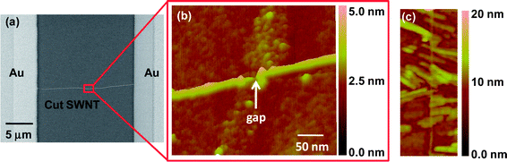 | ||
| Fig. 1 Micrographs of an individual SWNT with Au on Cr that has been cut using e-beam lithography and an oxygen plasma. (a) SEM micrograph of the SWNT after oxidatively cutting. (b) Tapping-mode AFM image of the gap cut into the SWNT. Inset shows the height profile of the isolated tube. The diameter of the SWNT is ∼2.6 nm, estimated from the height profile. (c) Tapping-mode AFM image of the device after CuPc monolayer deposition. The image is 350 nm × 900 nm in size. Inset shows the height profile of the image, which shows the average monolayer height of ∼1.3 nm. | ||
Depending on the different diameter and chirality of the tubes, SWNTs can be either metallic or semiconducting. Before cutting we scan the current–voltage characteristics of SWNT transistors and then categorize them as metallic or semiconducting. To aid in the subsequent analysis of the devices, we always chose those that are made from metallic SWNTs (lack of gate dependence). Fig. S1, ESI,† shows the comparison of the electrical properties of a metallic tube device before and after cutting. Before cutting, the electrical resistance of this device is ∼0.4 MΩ, and after cutting the device is open with the current down to the noise limit of the equipment (<100 fA).
CuPc monolayers were then vertically transferred from the water/air interface onto the substrate surface through the conventional LB technique (see experimental section). We found that homogenous high-coverage LB monolayers (height ∼1.3 nm, Fig. 1c) were easily formed in a face-to-face closely-stacking fashion with columnar structures that are nearly perpendicular to the substrate.28 The presence of the large size of CuPc monolayer domains makes it difficult to locate and image the nanogaps by AFM. Once nanoscale columns are formed to bridge the cut carbon nanotube electrodes and then nanoscale columnar transistors are formed (Scheme 1), it is reasonable that these columnar bridges could dominate the carrier transport characteristics of the devices. Because the diameter of these self-assembled columns (∼1.3 nm for CuPc) is comparable to the diameter of a typical SWNT (<3 nm), the maximum number of columns that the individual nanotube electrode can contact is three, even considering significant fringing fields near the electrodes. Given the size of the gap and the volume of the molecules assembled in this gap, we can estimate that the collective properties of ∼4–75 molecules are being probed (assuming that the pack of molecules is ∼0.4 nm,38 face-to-face, and is ∼1.3 nm in diameter).
All of the resultant nanodevices behaved as p-type, hole-transporting semiconductors. A set of the transistor characteristics for a representative device is shown in Fig. 2. Since Au/Cr metal electrodes have been protected by silicon dioxide, it is clear that the only pathway for charge transport is through SWNT electrodes bridged by CuPc LB monolayers. Fig. 2a shows output characteristics of the device as a function of gate bias. At the different gate voltage biases, we observed the superlinear increase in the drain current (ID) with the S/D voltage (VD) increase. Considering this observation, we extracted the carrier mobility in an unsaturated fashion from the drop of transfer characteristics of the device in Fig. 2b (see experimental section). The calculated linear mobility (μ) is ∼0.4 cm2V−1s−1 (L = 5 nm, W = 2.6 nm) with an ON/OFF current ratio as high as ∼4 orders when the OFF value is taken at VG = 50 V. This mobility value is ranked the highest among those obtained from organic ultrathin-film transistors (ref. 33 and references therein) and more than two orders of magnitude higher than those of CuPc LB monolayer transistors based on metal electrodes.39 This is significant, considering that the charge transfer transport in our monolayer transistors occurs from a single 1.3 nm-thick layer. The high ON/OFF current ratio explains how device characteristics of these nanodevices can be efficiently controlled by the gate voltage bias, even with thick gate dielectric (300 nm in our case), although short channel effects still influenced the device performance. Both the mobility and ON/OFF ratio are the critical parameters evaluating the quality of OFETs and has proved difficult to achieve such high values of these parameters in nanoscale devices made with metal electodes. In addition to the high carrier mobility and the high ON/OFF ratio described above, the yield of working devices is quite high, ∼80% out of ∼60 devices, thus making these results very reproducible and ensuring the successful fulfillment of the subsequent photoresponsive investigations. The subthreshold swing (S) in the device in Fig. 2 is ∼450 mV decade−1, which is similar to the values obtained by Dai's group34 and ours.36 The threshold voltage (VT) in these devices (∼47 working devices) is large (∼ +47 V), probably due to the shortened channel length and/or the high density of carrier traps at the interface between bare SiO2 and CuPc as described in the literature.40 Interestingly, although the length of nanogaps (effective channel length) varied from device to device (from 1 to 10 nm), no obvious relation was found between the length and the transistor characteristics of the devices. Due to the inevitable variables in devices, such as the diameter of the SWNTs and the quality of CuPc LB monolayers, the carrier mobility varied from 0.1 to 0.4 cm2V−1s−1 and the ON/OFF ratio from 103 to 104.
 | ||
| Fig. 2 Device characteristics of a representative device. (a) Output characteristics of the device. VG = 50 to −40 V in −18V steps. (b) Transfer characteristics of the device. VD = −6 V. L = ∼5 nm and W = ∼2.6 nm. (c) Time trace of the photocurrent of the same device under visible light irradiation. VG = 0 V and VD = −500 mV. (d) The time dependence of ID as the lights with different power were switched on and off. Inset is the power dependence of the changes in ID. VG = 0 V and VD = −50 mV. | ||
In general, it is difficult to detect the photoresponsive properties of monolayer transistors because of instantaneous detrimental charge recombination under light irradiation and the quenching of the photoexcited states of monolayer molecules exposed to the environments. Remarkably, in the current case we are able to measure their DC photoconductivity at room temperature in ambient atmosphere under light illumination. This is surprising because the photocurrent in the devices occurs within a single 1.3 nm-thick layer. As discussed before, SWNTs can form an excellent interface contact with molecules and exhibit barrier-free-like injection. Therefore, the application of relatively small voltages yields efficient charge injection in the gap area in the current case. This could significantly avoid detrimental charge recombination under light irradiation and the quenching effect by the environments, thus affording efficient charge transport through SWNT point contacts at low voltages and the high device photoresponsivities discussed below. The reversible photocurrent of the devices under irradiation of visible light (150W halogen lamp) was stable without obvious degradations through many measurement cycles even in the presence of oxygen and moisture in the air (Fig. 2c). We notice that the photocurrents varied slightly from device to device probably due to the different number of CuPc molecules in the nanogaps. Because of the comparable diameters between CuPc molecules and SWNTs, transport through columnar nanostructures of CuPc molecules inside the gap dominates the photocurrent, while molecules outside the gap have a negligible contribution. Although more than only the gap area is irradiated, outside the gap, the high barrier to intermolecular transport and the low field prevent significant contribution to photocurrent. The response time is reasonably short, ∼5 s, probably because of the diffusion processes and/or large capacitive components. The power dependence of the photocurrent of the same device is shown in Fig. 2d. With the increase of light power, the drain current (ID) of the device gradually saturates, indicating that the photoinduced carrier density has reached its maximum.
To ensure that the path of photocurrent is through the nanojunctions between SWNT electrodes and CuPc monolayers, we tested a number of devices that have been fully cut but lack CuPc monolayers and the devices formed from CuPc monolayers between metal electrodes. None of these devices showed obvious photoeffects under light illumination. To further understand the important role of CuPc monolayers in device photoconductivity, we carried out wavelength-dependent measurements. Based on the device photocurrent (Fig. S2, ESI†), we calculated the responsivities (R) in order to indicate the intrinsic photosensitivity of the devices by using the conventional model for the calculation

 | ||
| Fig. 3 Photoresponsive characteristics of monolayer photodetectors. (a) The comparison of the wavelength-dependent spectrum of the responsivities for the device used in Fig. 2 with the UV/vis absorption spectrum of 50 nm thick CuPc thin films deposited by thermal evaporation. Light was scanned from 500 to 800 nm in 5 nm steps with each wavelength left on for 5 s. All wavelengths used here were adjusted to be constant, ∼240 μW cm−2. VG = 0 V and VD = −800 mV. (b) Responsivities versus wavelength and calculated detectivities at λ = 620 nm and λ = 702 nm at various biases for another device. Inset is the tapping-mode AFM image of the device showing the gap size of ∼8 nm (L) and the tube diameter of ∼2.5 nm (W). VG = 0 V. (c) Bias-dependent data of responsivities and detectivities for the same device excited using a 620 nm light. VG = 50 to −40 V in −18 V steps. (d) LDR of the same device under visible light irradiation. Inset is the dark current of the device. VG = 0 V and VD = −20 mV. | ||
Interestingly, the device photoresponsivity is bias-dependent. Fig. 3b shows the responsivity data of another similar device as a function of light wavelength at various S/D biases and a fixed gate bias. Again, the reproducible similarity between the responsivity and absorption spectra demonstrates the fact that monolayer molecules in the nanogaps do indeed contribute to the photocurrent. Fig. 3c shows the measured responsivity as a function of the applied biases for the same device excited using a 620 nm light, which has the spectral structure similar with the transistor characteristics. Varying S/D and gate biases results in the gradual improvements of the responsivity values, indicating the fine-tunability of the device photoresponsivity. These results suggest that the three-terminal transistor geometry might be superior to the commonly-used two-terminal device structures for improving the photodetector performance.
Another important parameter to quantify the photodetector sensitivity is D*, the detectivity measured in units of Jones. D* is given by the following (AΔf)1/2R/in, where A is the effective area of the detector in cm2, Δf the electrical bandwidth in Hz, and R the responsivity in A W−1 measured under the same conditions as the noise current in (in amperes). This material feature of merit D* allows us to compare the quality of devices with different areas and geometries. The photodetector feature of merit, noise equivalent power (NEP), i.e., the minimum impinging optical power that a detector can distinguish from noise, is related to D* by NEP = (AΔf)1/2/D*. Among the factors contributing to the noise that limits D* (shot noise from the dark current, Johnson noise, generation–recombination noise, and thermal fluctuation “flicker” noise),43,44 if, as expected, the shot noise from the dark current is the major contribution in our case, D* can be expressed by the following D* = R/(2qJdark)1/2 = R/(2qIdark/S)1/2, where q is the absolute value of electron charge (1.6 × 10⁻¹⁹ Coulombs), Jdark the dark current density, and S the effective area of the device. Based on the measured photocurrent, dark current (Fig. S5, ESI†), and incident light intensity, detectivities were then calculated using this equation for the monolayer transistors with SWNT point contacts. At VG = 0 V, the calculated detectivities are D* = ∼ 2.0 × 10¹⁵ Jones, ∼ 2.3 × 10¹⁵ Jones, and ∼ 3.2 × 10¹⁵ Jones under irradiation at 620 nm and ∼ 1.9 × 10¹⁵ Jones, ∼ 2.1 × 10¹⁵ Jones, and ∼ 2.6 × 10¹⁵ Jones under irradiation at 702 nm, with light intensity of 240 μW cm−2 at various S/D biases (from −1.5 V to −2.4 V and −2.9 V), respectively (Fig. 3b). Fig. 3c also shows the bias-dependent data of the detectivity for the same device excited using a 620 nm light. The best detectivities (>7 × 10¹⁵ Jones) were obtained at higher S/D and gate biases, which also led to the highest responsivities (>108 A W−1). This strong photoresponse might be due to an integrated mechanism, for example, due to build-up of electron-trapped charges at the semiconductor/dielectric interface during illumination over several seconds. These results clearly demonstrated that high detectivities require not only high photoresponsivity (high photocurrent) but also low noise (low dark current). However, these values are just for comparison with conventional photodetectors because we use the same conventional model for the calculation,43,44 which might not be accurate here.
Another photodetector feature of merit is the linear dynamic range (LDR) or photosensitivity linearity (typically quoted in dB). LDR is given by LDR = 20log(I*ph/Idark), where I*ph is the photocurrent, measured at light intensity of 1 mW cm−2. Fig. 3d shows the photocurrent versus the light intensity for the monolayer transistor used above. Under illumination with visible light from a 150W halogen lamp, the calculated LDR is ∼35 dB, which is less than those obtained from Si photodetectors (120 dB) and InGaAs photodetectors (66dB). These modest LDR values are limited by the relatively low ratio of photocurrent versus dark current, thus leaving room for future improvement.
Conclusion
In this work we detailed a method to make efficacious monolayer photodetectors through combination of bottom-up self-assembly and top-down device fabrication. By using 1D ballistic SWNTs as point contacts, these photodetectors formed from water-processed LB monolayers of CuPc show superhigh sensitivity and can operate at room temperature with low-power consumption and high yield. The ease of device fabrication, the reproducibility, and the achievement of the photoresponsivity and detectivity results might open new attractive opportunities for the creation of low-cost, high-resolution detector arrays for a variety of possible sensor applications including chemical/biological imaging, environmental monitoring, telecommunication, and day- and night-time surveillance.Experimental
SWNT transistor fabrication
Individual SWNTs of high electrical quality (diameter <3 nm) were grown by a chemical vapor deposition (CVD) process from CoMo-doped mesoporous SiO2 catalyst particles using ethanol as the carbon source.30 The catalyst particles were patterned onto a doped silicon wafer that have 300 nm of thermally grown SiO2 on the surface. Au/Cr contact pads (5 nm of Cr followed by 50 nm of Au) separated by ∼20 μm were deposited through a metal shadow mask onto the carbon nanotube samples using a thermal evaporator. The doped silicon wafer serves as a global back-gate electrode for the samples. After the initial electric characterization, we selected individual metallic carbon nanotube devices to do all of the next experiments.Cutting procedure
After device fabrication and characterization, a PMMA layer (950, A2) was spincast (4000 PRM, 45 s) on the surface and then baked at 170 °C for 2 min. Using e-beam lithography, we run a DesignCAD file with around 5 nm width line at the specific position to obtain the window precursor. Then a mixture of water/isopropanol (1![[thin space (1/6-em)]](https://www.rsc.org/images/entities/char_2009.gif) :3) is used for the liftoff at 5 °C for 1 min with the aid of sonication. After liftoff, the devices were washed by deionized (DI) water and dried with a stream of N2 gas. After the window was opened, the devices were put into an ME-3A RIE machine. The nanotubes were then locally cut through the open window by oxygen plasma (50 W RF power, oxygen 250 mTorr, for 10 s). After cutting the devices were soaked in acetone solution overnight, removed, washed by acetone, isopropanol, DI water, and dried with a stream of N2 gas. Under these optimized conditions, ∼20–25% of the tubes were completely cut. Based on the previous results,30–32 the statistical variability of the plasma etch process creates ensembles of nanotube devices with gaps in the 1–10 nm range.
:3) is used for the liftoff at 5 °C for 1 min with the aid of sonication. After liftoff, the devices were washed by deionized (DI) water and dried with a stream of N2 gas. After the window was opened, the devices were put into an ME-3A RIE machine. The nanotubes were then locally cut through the open window by oxygen plasma (50 W RF power, oxygen 250 mTorr, for 10 s). After cutting the devices were soaked in acetone solution overnight, removed, washed by acetone, isopropanol, DI water, and dried with a stream of N2 gas. Under these optimized conditions, ∼20–25% of the tubes were completely cut. Based on the previous results,30–32 the statistical variability of the plasma etch process creates ensembles of nanotube devices with gaps in the 1–10 nm range.
Monolayer transistor formation and characterization
CuPc was purchased from the Aldrich Corporation and used after further sublimation purification. Surface pressure-area isotherm measurements and monolayer deposition experiments were performed on a fully automatic KSV-5000 instrument (Finland). CuPc solutions were spread onto pure water. The monolayer was formed by moving the Teflon barrier with a compression rate of 5 mm min−1. At a constant pressure of 20 mN m−1, the floating CuPc monolayers on the subphase were transferred to the Si/SiO2 substrate by the vertical method. The transfer ratio is 1.0 ± 0.1. The CuPc LB monolayers were analyzed by AFM using a Nanoscope III Scanning Probe Microscope with silicon cantilevers in the tapping mode. The devices were characterized by using a Karl Suss (PM5) manual probe station equipped with a semiconducting parameter analyzer (Agilent 4155C). At low VD, ID increases linearly with VD (unsaturation regime) and is approximately determined by the following equation: ID = WCiμVD(VG−VT−VD/2)/L, where W is the channel width, L the channel length, and Ci the gate dielectric capacitance (per area). The carrier mobility (μ) were then calculated in the linear regime from the transconductance, , by plotting IDversus VG at a constant low VD and equating the value of the slope of this plot to gm. Power-dependent experiments were performed with a 150 W Halogen incandescent lamp. Wavelength-dependent experiments were performed by using a TLS1509-150A light source with a 150W Xe lamp (Zolix instruments Ltd., Beijing). To avoid the heating effect during irradiation, lights were focused and guided by a long optical fiber to the devices separated by ∼2 cm. All wavelengths used here were adjusted to be constant, ∼240 μW cm−2. All of the measurements were performed under the same conditions and at the same temperature. The light power intensity was measured by using an LPE-1A optical power meter (Physcience Opto-Electronics, Ltd., Beijing) in the same experimental condition.
Acknowledgements
We thank Zhongfan Liu for enlightening discussions. We acknowledge primary financial support from FANEDD (No. 2007B21), 111 Project (B08001), BSTSP (2009A01), MOST (2009CB623703 and 2008AA062503) and NSFC (Grant No. 50873004, 50821061, and 20833001).Notes and references
- S. Hoogland, V. Sukhovatkin, I. Howard, S. Cauchi, L. Levina and E. H. Sargent, Opt. Express, 2006, 14, 3273–3281 CrossRef CAS.
- M. Ettenberg, Adv. Imaging, 2005, 20, 29–32 Search PubMed.
- E. H. Sargent, Adv. Mater., 2005, 17, 515–522 CrossRef CAS.
- S. Kim, Y. T. Lim, E. G. Soltesz, A. M. De Grand, J. Lee, A. Nakayama, J. A. Parker, T. Mihaljevic, R. G. Laurence, D. M. Dor, L. H. Cohn, M. G. Bawendi and J. V. Frangioni, Nat. Biotechnol., 2004, 22, 93–97 CrossRef.
- X. Gong, M. H. Tong, Y. J. Xia, W. Z. Cai, J. S. Moon, Y. Cao, G. Yu, C. L. Shieh, B. Nilsson and A. J. Heeger, Science, 2009, 325, 1665–1667 CrossRef CAS.
- J. F. Wang, M. S. Gudiksen, X. F. Duan, Y. Cui and C. M. Lieber, Science, 2001, 293, 1455–1457 CrossRef CAS.
- H. Kind, H. Q. Yan, B. Messer, M. Law and P. D. Yang, Adv. Mater., 2002, 14, 158–160 CrossRef CAS.
- S. Han, W. Jin, D. H. Zhang, T. Tang, C. Li, X. L. Liu, Z. Q. Liu, B. Lei and C. W. Zhou, Chem. Phys. Lett., 2004, 389, 176–180 CrossRef CAS.
- Y. Ahn, J. Dunning and J. Park, Nano Lett., 2005, 5, 1367–1370 CrossRef CAS.
- J. Barton, R. Cannata and S. Petronio, Proc. SPIE–Int. Soc. Opt. Eng., 2002, 4721, 37–47 CAS.
- J. Wu, D. L. Shao, V. G. Dorogan, A. Z. Li, S. B. Li, E. A. DeCuir, M. O. Manasreh, Z. M. Wang, Y. I. Mazur and G. J. Salamo, Nano Lett., 2010, 10, 1512 CrossRef CAS.
- S. A. McDonald, G. Konstantatos, S. G. Zhang, P. W. Cyr, E. J. D. Klem, L. Levina and E. H. Sargent, Nat. Mater., 2005, 4, 138–142 CrossRef CAS.
- G. Konstantatos, I. Howard, A. Fischer, S. Hoogland, J. Clifford, E. Klem, L. Levina and E. H. Sargent, Nature, 2006, 442, 180–183 CrossRef CAS.
- T. Rauch, M. Boberl, S. F. Tedde, J. Furst, M. V. Kovalenko, G. N. Hesser, U. Lemmer, W. Heiss and O. Hayden, Nat. Photonics, 2009, 3, 332–336 CrossRef CAS.
- S. R. Forrest, Nature, 2004, 428, 911–918 CrossRef CAS.
- G. Yu, J. Gao, J. C. Hummelen, F. Wudl and A. J. Heeger, Science, 1995, 270, 1789–1791 CrossRef CAS.
- G. Yu, J. Wang, J. McElvain and A. J. Heeger, Adv. Mater., 1998, 10, 1431–1434 CrossRef CAS.
- G. A. O'Brien, A. J. Quinn, D. A. Tanner and G. Redmond, Adv. Mater., 2006, 18, 2379–2383 CrossRef CAS.
- P. Peumans, V. Bulovic and S. R. Forrest, Appl. Phys. Lett., 2000, 76, 3855–3857 CrossRef CAS.
- P. Schilinsky, C. Waldauf and C. J. Brabec, Appl. Phys. Lett., 2002, 81, 3885–3887 CrossRef CAS.
- W. U. Huynh, J. J. Dittmer and A. P. Alivisatos, Science, 2002, 295, 2425–2427 CrossRef CAS.
- Y. Wang and N. Herron, Chem. Phys. Lett., 1992, 200, 71–75 CrossRef CAS.
- H. Mattoussi, L. H. Radzilowski, B. O. Dabbousi, E. L. Thomas, M. G. Bawendi and M. F. Rubner, J. Appl. Phys., 1998, 83, 7965–7974 CrossRef CAS.
- J. S. Steckel, S. Coe-Sullivan, V. Bulovic and M. G. Bawendi, Adv. Mater., 2003, 15, 1862–1866 CrossRef CAS.
- I. W. Hwang, C. Soci, D. Moses, Z. G. Zhu, D. Waller, R. Gaudiana, C. J. Brabec and A. J. Heeger, Adv. Mater., 2007, 19, 2307–2312 CrossRef CAS.
- D. Natali, M. Sampietro, M. Arca, C. Denotti and F. A. Devillanova, Synth. Met., 2003, 137, 1489–1490 CrossRef CAS.
- Y. Yao, Y. Y. Liang, V. Shrotriya, S. Q. Xiao, L. P. Yu and Y. Yang, Adv. Mater., 2007, 19, 3979–3983 CrossRef CAS.
- Z. Wei, W. Xu, W. Hu and D. Zhu, Langmuir, 2009, 25, 3349–3351 CrossRef CAS.
- K. Xiao, R. J. Li, J. Tao, E. A. Payzant, I. N. Ivanov, A. A. Puretzky, W. P. Hu and D. B. Geohegan, Adv. Funct. Mater., 2009, 19, 3776 CrossRef CAS.
- X. Guo, P. S. Joshua, E. K. Jennifer, Y. Wang, S. Purewal Meninder, W. Tam Iris, H. Hong Byung, R. Caldwell, L. Huang, S. O'Brien, J. Yan, R. Breslow, J. W. Shalom, J. Hone, P. Kim and C. Nuckolls, Science, 2006, 311, 356–359 CrossRef CAS.
- A. K. Feldman, M. L. Steigerwald, X. Guo and C. Nuckolls, Acc. Chem. Res., 2008, 41, 1731–1741 CrossRef CAS.
- X. Guo, A. A. Gorodetsky, J. Hone, J. K. Barton and C. Nuckolls, Nat. Nanotechnol., 2008, 3, 163–167 CrossRef CAS.
- Y. Cao, M. L. Steigerwald, C. Nuckolls and X. Guo, Adv. Mater., 2010, 22, 20–32 CrossRef CAS.
- P. Qi, A. Javey, M. Rolandi, Q. Wang, E. Yenilmez and H. Dai, J. Am. Chem. Soc., 2004, 126, 11774–11775 CrossRef CAS.
- K. Tsukagoshi, I. Yagi and Y. Aoyagi, Appl. Phys. Lett., 2004, 85, 1021–1023 CrossRef CAS.
- X. Guo, M. Myers, S. Xiao, M. Lefenfeld, R. Steiner, G. S. Tulevski, J. Tang, J. Baumert, F. Leibfarth, J. T. Yardley, M. L. Steigerwald, P. Kim and C. Nuckolls, Proc. Natl. Acad. Sci. U. S. A., 2006, 103, 11452–11456 CrossRef CAS.
- C. M. Aguirre, C. Ternon, M. Paillet, P. Desjardins and R. Martel, Nano Lett., 2009, 9, 1457–1461 CrossRef CAS.
- A. Hoshino, Y. Takenaka and H. Miyaji, Acta Crystallogr., Sect. B: Struct. Sci., 2003, 59, 393–403 CrossRef.
- Z. Wei, Y. Cao, W. Ma, C. Wang, W. Xu, X. Guo, W. Hu and D. Zhu, Appl. Phys. Lett., 2009, 95, 033301–033303 CrossRef.
- Y. Cao, S. Liu, Q. Shen, K. Yan, P. Li, J. Xun, D. Yu, M. L. Steigerwald, C. Nuckolls, Z. Liu and X. Guo, Adv. Funct. Mater., 2009, 19, 2743–2748 CrossRef CAS.
- K. Xiao, Y. Liu, X. Huang, Y. Xu, G. Yu and D. Zhu, J. Phys. Chem. B, 2003, 107, 9226–9230 CrossRef CAS.
- M. Freitag, Y. Martin, J. A. Misewich, R. Martel and P. Avouris, Nano Lett., 2003, 3, 1067–1071 CrossRef CAS.
- A. R. Jha, Infrared Technology (Wiley, New York), 2000, 245–359 Search PubMed.
- P. Bhattacharya, Semiconductor Optoelectronics Device (Prentice-Hall, Upper Saddle River, NJ), 1997, 345–367 Search PubMed.
Footnote |
| † Electronic supplementary information (ESI) available: Figs. S1 to S5. See DOI: 10.1039/c0sc00488j |
| This journal is © The Royal Society of Chemistry 2011 |