Rapid prototyping of poly(dimethoxysiloxane) dot arrays by dip-pen nanolithography†
Aaron
Hernandez-Santana
,
Eleanore
Irvine
,
Karen
Faulds
and
Duncan
Graham
*
Centre for Molecular Nanometrology, WestCHEM, Department of Pure and Applied Chemistry, University of Strathclyde, 295 Cathedral Street, Glasgow, G1 1XL, UK. E-mail: duncan.graham@strath.ac.uk; Fax: +44 (0)141 548 4787; Tel: +44 (0)141 548 4701
First published on 17th November 2010
Abstract
We report the first direct patterning of elastomeric PDMS structures by dip-pen nanolithography (DPN). This method involves the use of a cantilever tip to transfer a PDMS ink onto a silicon dioxide surface to create dot array patterns which are then cross-linked and bonded irreversibly to the substrate. The chemical composition of the PDMS structures deposited by DPN was characterised by Raman microspectroscopy to provide an insight into the ink transfer process. This technique offers a significant advance in the ability to rapidly and easily produce programmable surface features from a widely used polymer for use in a variety of applications.
Introduction
Poly(dimethoxysiloxane) (PDMS) is one of the most widely used silicon based organic polymers. In fact, it is a common component in lubricants, sealants, foodstuffs, implants, and health and beauty products.1 PDMS is relatively inexpensive, readily available, nontoxic, chemically inert, transparent and odourless. Soft-lithography techniques such as microcontact printing (μCP) employ PDMS to create micro- and nanoscale structures.2 It is usually patterned by a moulding process and used as a master for pattern transfer. Firstly, a mask is generated using photo or electron beam lithography, which can be expensive and time-consuming. PDMS is then poured over the master, cured and removed to obtain a negative structure. Unlike photoresists, PDMS may be cured at room temperature and does not require ultraviolet light to cross-link. The patterned elastomeric stamp can then be used to transfer chemical inks onto a surface. PDMS is also a popular material of choice in the fabrication of microfluidic systems for flow delivery and biomedical diagnostics.3Dip-pen nanolithography (DPN) is a versatile and powerful nano and micro fabrication technique capable of patterning a wide range of materials on an equally extensive variety of surfaces.4 A number of review articles have been reported in this field of research.5,6 In this technique, a sharp cantilever tip (AFM tip) is used to transport chemical “inks” when placed in contact with a suitable surface. However, this is not strictly a requisite and close-contact (tapping mode) has been proposed as a method for material deposition.7 In the context of DPN, PDMS has been used to develop techniques such as scanning probe contact printing (SP-CP), where a commercial scanning probe microscope (SPM) with an integrated elastomeric PDMS tip was used to transfer chemicals onto a substrate.8 Further work by Mirkin and co-workers led to the development of polymer-pen lithography (PPL) in which a 2D array containing thousands to millions of elastomeric tips are used to pattern surfaces in a high-throughput manner.9
In this work, however, we have used DPN to produce the first direct patterning of a PDMS-based ink onto silicon dioxide surfaces. Once patterned, the structures are cured and bonded irreversibly to the substrate. PDMS has been printed on paper using a dot plotter to produce hydrophilic barriers as channels for fluid containment but the minimum size of the printed features was ∼1 mm.10 The direct-write method of DPN allows the fast and controlled fabrication of PDMS structures of micrometer dimensions with piezo-controlled placement capability and registry.
Results and discussion
One of the key initial steps in our method involved the formulation of a suitable PDMS ink composition for use in DPN. PDMS is normally supplied as a two-part kit, composed of a pre-polymer base and a curing agent which are then mixed in a 10![[thin space (1/6-em)]](https://www.rsc.org/images/entities/char_2009.gif) :1 ratio (wt/wt), respectively. Once combined, the mixture has a pot-life (time taken for viscosity to double) of approximately 2 h. Nevertheless, this mixture will take ∼48 h at room temperature to form a solid crosslinked polymer and will remain in the liquid state throughout the patterning process.
:1 ratio (wt/wt), respectively. Once combined, the mixture has a pot-life (time taken for viscosity to double) of approximately 2 h. Nevertheless, this mixture will take ∼48 h at room temperature to form a solid crosslinked polymer and will remain in the liquid state throughout the patterning process.
The DPN tip may be coated with a “chemical ink” in a variety of ways including dip-coating, vapour coating, and through the use of microfluidic inkwells. We opted for the latter approach for a number of practical reasons including the ability to coat different tips with multiple inks at once when using a one dimensional (1D) 12-tip array and the possibility to re-ink the tips when required.11 The main drawback of this method was that PDMS is a viscous liquid, with a viscosity resembling that of a syrup (3900 cP), which prevented it from flowing in the microfluidic channels. However, it can be easily diluted in hexane and other organic solvents in order to decrease its viscosity.12Hexane is considered to be a good, compatible solvent for diluting the PDMS prepolymer in applications such as spin casting of thin films.13,14,15 We determined the appropriate dilution of the PDMS mixture in hexane by varying their proportions. Different PDMS dilutions 0–40% hexane (wt/wt) were loaded into the inkwells and the most consistent results were obtained when the base PDMS mixture was diluted with hexane at 30% (wt/wt). This ink formulation was used throughout our experiments and was observed to remain “wet” inside the microfluidic inkwell during the patterning process.
The fabrication process for PDMS structures deposited by DPN is illustrated in Fig. 1. The tip was first coated with the PDMS ink by submerging it into the inkwell for five seconds, after which the polymer was immediately patterned on a silicon dioxide surface. Tip-surface position was controlled by computer software and a piezoelectric (x-y-z) scanner stage, which allows the fabrication of custom designed patterns.
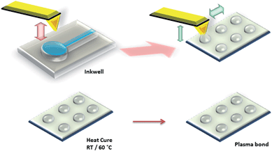 | ||
| Fig. 1 Schematic representation of the DPN procedure used to pattern PDMS on a silicon dioxide substrate. | ||
Unlike other traditional DPN-based experiments found in the literature, patterning was performed without force-feedback (AFM), where a laser reflecting off the probe ensures that constant force is applied with respect to the substrate surface. Tip-surface contact and array levelling was accomplished through visual observation of the tip deflection, characterised by a sharp change in tip reflectivity upon contact with the surface. Under this condition, the DPN deposition process is regarded to be effectively force independent.16
The PDMS arrays were heat cured at 60 °C for one hour to finalise the crosslinking process. Once cured, PDMS can be easily bonded either reversibly or irreversibly to a range of materials including glass, silicon and PDMS itself.17 When exposed to an oxygen plasma, Si–CH3 groups along the PDMS backbone are transformed into hydrophilic Si–OH groups by the reactive oxygen species. However, hydrophobicity is recovered soon after when placed back in air.18 If desired, surface silanisation may be achieved by immediately exposing the silanol surface to alkoxysilanes containing functional headgroups to obtain surface properties and functionalities of choice.17Oxygen-plasma treatment of PDMS can lead to the formation of a smooth oxidised surface layer of >100 nm in thickness19 and we used this method to permanently bond the PDMS structures patterned by DPN to the underlying silicon dioxide substrate. The bonding mechanism is poorly understood but it is considered to involve breaking of bonds on each surface during treatment followed by the formation of Si–O–Si bonds.
DPN was used to pattern custom designed PDMS spot arrays with excellent control and high throughput (Fig. 2). The contact time between the PDMS coated tip and the substrate surface, also known as the dwell time, was alternated between 0.25 and 0.1 s to produce the features illustrated in Fig. 2 (b). Close-contact AFM analysis was used to determine the size of the features, which showed a difference in both spot diameter and feature height depending on the dwell time used, with the longer dwell time producing larger features. AFM topographical analysis did not show delamination or deformation at the edges of the features after oxygen-plasma treatment, suggesting successful bonding to the underlying substrate.
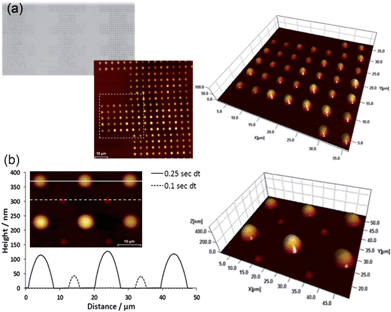 | ||
| Fig. 2 (a) Optical image and overlaid AFM topography images of programmable patterning of PDMS structures by DPN. (b) Overlaid height profile of PDMS spots created by using alternating dwell times of 0.25 and 0.1 s (first two rows). Inset and adjacent image: AFM topography image of PDMS spots used in (b). | ||
The deposition process was examined in more detail by systematically varying the dwell time from 0.1 to 1 s. Ink transport is assumed to occur due to 2-D surface diffusion from the tip to the substrate, where the dot diameter of the features should follow a square root dependence on dwell time.20Fig. 3 shows plots of changes in spot diameter and height as a function of dwell time (plotted as √t) from AFM analysis data. The smallest features achieved by this method were 2.7 μm in diameter and only 18.6 nm in height when using a dwell time of 0.1 s. The deposition process follows a linear increase in spot diameter for dwell times up to 0.75 s but did not seem to increase with longer dwell times. This non-linear phenomenon at longer dwell times has been observed for other liquid inks used in DPN, where further contact time with the surface will not increase feature size.21,22 We observed a linear increase (R2 = 0.99) in feature height for the dwell time range used in this study. The largest features obtained in this study produced features of about 13.96 μm in diameter and 376.4 nm in height at 1 s dwell time. We have shown that it is effectively possible to generate PDMS features with a range of dimensions (2.7–13.9 μm diameter, 18.6–376.4 nm height) by simply varying the tip-substrate contact time. Furthermore, the use of 1D arrays containing 12 individual tips makes it possible to pattern large areas in a very short period of time.
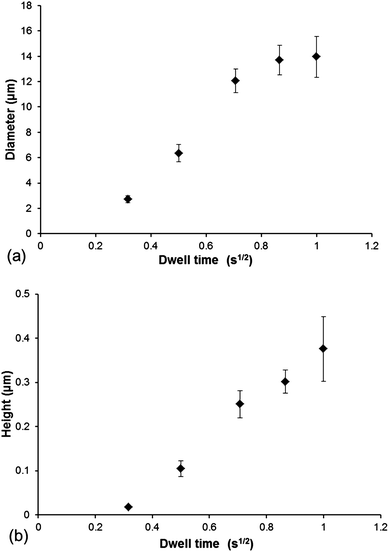 | ||
| Fig. 3 (a) Plot of dwell time vs. spot diameter and (b) plot of dwell time vs. feature height. | ||
Traditionally, DPN experiments have been centred on the patterning of thiols on Au surfaces. This combination of ink-surface is characterised by chemisorption of the thiol molecules on the Au surface to form Au–S bonds. Mercaptohexadecanoic acid (MHA) and octadecanethiol (ODT) are common examples of alkanethiols that have been studied under ambient conditions.20 Unlike the liquid ink used in this study, the ink is chemisorbed onto the tip in a dry state by dip-coating or vapour coating. It has been suggested that the water meniscus found at the tip-surface interface is then used as a medium for ink transport, where the ink deposition rate is influenced by parameters such as humidity and temperature.23,24 In this regard, some studies suggest that ink transfer is related to the solubility of the ink in water.25 However, the transport rate of MHA and ODT as model molecular inks was examined under atmospheres of different organic vapours and it was found that this increased deposition rate and feature size by up to one order of magnitude.26 This suggests that the exact mechanism of ink transport is still not fully understood and that other mechanisms can take place apart from bulk meniscus transfer. A number of models have been proposed but unfortunately they have been centred almost exclusively on thiol/Au systems involving a water meniscus.27,28
Several examples in literature have used aqueous based additives such as Tween-20,29glycerol,21agarose,22poly(ethylene glycol),30 to carry biomolecules and nanomaterials. The role of these additives range from preventing biomolecule denaturation to increasing the wettability of the substrate and the viscosity of the ink formulation. Alternatively, the surface properties of the cantilever tip itself may be chemically modified to control transfer of materials.31 The PDMS ink used in this study is already in the liquid phase and is immiscible with water, so this process might not require a water meniscus for transport. PDMS is hydrophobic and viscous so this facilitates ink adsorption onto the hydrophobic silicon nitride tip. The ink transfer behaviour of the PDMS ink appears to be in relative agreement with other viscous liquid inks reported in literature, where ink transfer seems to be dominated at two key points of the writing process: (a) wetting/loading of the tip with the ink, (b) transfer of the ink from the tip onto the substrate surface. It has been recognized that feature size of liquid inks deposited by DPN is dictated by factors such as physisorption (unlike thiols on Au where chemisorption is involved) and surface tension between the ink and the substrate surface.21,32 For instance, a non-wetting surface can present an additional activation barrier for ink transport. The use of surfactants as additives in ink formulations provide a means of controlling ink transfer by increasing the wettability of the substrate.29 Viscosity plays an important role in the DPN process of various liquid inks.21,22,33 Studies based on thiol inks patterned on Au by DPN have shown that the ink transport properties can be greatly affected by the hydrophobicity of the substrate. For instance, ink transport of ODT deposited over an existing MHA layer was almost twice as fast as when compared to the bare gold surface.34 Although we did not carry out an extensive study of different surfaces, we support that the surface properties of the substrate will play an important role in dictating liquid PDMS ink transport and ultimately feature size.
In most cases, the actual composition and relative concentrations of the components present in the bulk ink preparation compared to that of the ink ultimately deposited on the substrate is unknown. When patterning binary mixtures of MHA and ODT alkanethiols, phase separation has been reported, where the more hydrophilic alkanethiol always forms the interior phase, while the hydrophobic alkanethiol will form the outer phase.35 This report described phase separation at the substrate surface but this is also likely to occur at the liquid-tip interface during the tip coating procedure. In order to establish whether phase separation of the different PDMS ink components occurred when using DPN as the deposition method, a small drop (∼1 μL) of the same PDMS ink formulation was placed with a micropipette onto the silicon dioxide surface. The droplet was then cured and bonded to the substrate in the same manner as done for the DPN-based arrays. Raman spectroscopy was our chosen method of chemical analysis.
Raman spectroscopy is a non-invasive method of chemical analysis that enables real-time reaction monitoring and characterisation of compounds.36 In a typical measurement, the sample is illuminated with a laser and the scattered light is collected and analysed. The wavelengths and intensities of the scattered light can be used to identify functional groups in a molecule. The integration of a microscope with Raman systems provides access to confocal techniques, which allow spectra to be collected from a very small volume (<1 μm in diameter). Confocal Raman spectroscopy allowed us to carry out non-destructive analysis of the elastomeric materials deposited by DPN.
A microscope was used to focus the laser beam and obtain chemical characterisation of single PDMS droplets and microspots. Fig. 4 shows a sample Raman spectrum of the PDMS material deposited as a droplet using a micropipette, which was typical of Raman spectra obtained previously by others.37 Si–O–Si stretching vibrations appear at 492 cm−1, Si–CH3 rocking vibrations appear at 708 cm−1, CH3 bending vibrations appear at 1263 and 1412 cm−1, and CH3 stretching vibrations appear at 2905 and 2965 cm−1. The peak vibration frequencies obtained for the PDMS droplet were in agreement with the corresponding microspot deposited by DPN (Table 1). The relative intensity of the methyl stretch vibrations of PDMS have been shown to be sensitive to the polymer conformation and can be used to assess changes in molecular structure.37 The inset in Fig. 4 compares the relative intensity of the Raman bands in the methyl stretch region (symmetric and asymmetric carbon–hydrogen stretch at 2905 cm−1 and 2965 cm−1) for each type of preparation, which show a similar peak ratio intensity. Further to this, we were able to generate chemical composition maps of PDMS microspots based on the Raman intensity of a relevant vibration of choice (symmetric methyl stretch, Fig. 4 (b & c)), confirming the chemical identity of the structures and their relative spatial positions on the surface.
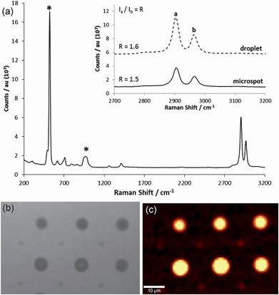 | ||
| Fig. 4 (a) Raman spectrum of PDMS spot cured onto the silicon dioxide substrate. Raman bands originating from the silicon substrate are marked with a star. Inset: Comparison of the relative intensity of the Raman bands found in the methyl stretch region for the PDMS drop and microspot. (b) Bright-field image of PDMS structures deposited by DPN using alternating dwell times of 0.25 and 0.1 s and (c) Raman map (CH3 stretch region) of the same alternating features. | ||
| Band assignment | PDMS droplet | PDMS microspot |
|---|---|---|
| Si–O–Si symmetric stretching | 492 cm−1 | 491 cm−1 |
| Si–C asymmetric rocking | 708 cm−1 | 709 cm−1 |
| CH3 bending | ||
| Symmetric | 1263 cm−1 | 1262 cm−1 |
| Asymmetric | 1412 cm−1 | 1412 cm−1 |
| CH3 stretching | ||
| Symmetric | 2905 cm−1 | 2905 cm−1 |
| Asymmetric | 2965 cm−1 | 2964 cm−1 |
DPN has been previously used to generate nanostructures on gold for use as lithographic masters.38 To further demonstrate the versatility of our approach we used a PDMS array deposited on silicon dioxide by DPN as a master for replication in soft lithography (Fig. 5). In fact, it has been shown that PDMS masters reinforced with silicon dioxide plates can reduce residual and deflecting deformations encountered during pattern transfer.39 In this particular example, PDMS arrays were first patterned using a 0.1 s dwell time and a 10 μm pitch onto a silicon dioxide surface to create a master. Freshly prepared PDMS prepolymer (10:1 mixture, no hexane) was then poured over the master and left to cure at room temperature over 48 h. The crosslinked PDMS replica was then peeled off and analysed by AFM. Feature transfer was readily observed under a light microscope. In practice, the master is left intact and ready to produce more replicas. Masks made using photoresists would normally require a larger amount of polymer to pattern a given area, with unexposed material removed and going to waste during the developing process.
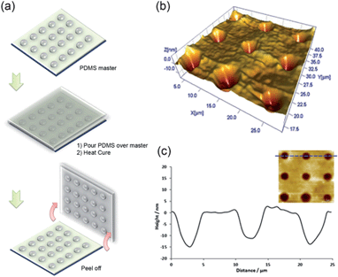 | ||
| Fig. 5 (a) Schematic representation of the procedure to fabricate a PDMS negative replica from a PDMS master prepared by DPN. (b) 3D AFM topography image of negative features transferred onto the PDMS replica and (c) height profile for three negative structures showing voids in the surface. | ||
Conclusions
We have demonstrated the first direct-write method for patterning PDMS structures with micrometer dimensions and arbitrary geometries using DPN. The PDMS prepolymer was dissolved in hexane in order to allow flow into a microfluidic inkwell and ink transfer onto a silicon dioxide surface. Silicon dioxide was used as a substrate due to its wide availability and the possibility to permanently bond the structures to the surface through plasma treatment. PDMS structures with dimensions ranging from 2.7–13.9 μm in diameter and 18.6–376.4 nm in height were fabricated using dwell times of less than 1 s, illustrating the flexibility with regards to feature size control provided by this method. The use of short dwell times and 1D arrays of DPN probes (12 tips) allow for an increase in overall patterning throughput and rapid prototyping of PDMS structures. Raman microspectroscopy was used to analyse and compare the chemical composition of the PDMS arrays against the bulk preparation and it was concluded that phase separation of the ink components was not apparent under the conditions used. This advance provides a massive step forward in terms of the ability to develop PDMS structures for BioMEMS applications and the example given of a PDMS array fabricated by DPN used as a replication master indicates the potential for many other applications.Experimental section
Materials and methods
Hexane was purchased from Sigma-Aldrich, UK. The elastomeric kit used in this work (Sylgard 184, Dow Corning Corporation) is composed of a two-component heat curing system, consisting of a pre-polymer (base) and a cross-linker (curing agent). In this study, pre-polymer (1.0 g) was mixed thoroughly with the curing agent in the weight ratio of 10:1. The PDMS mixture was then diluted with n-hexane to give a 30% (wt/wt) mixture.
PDMS array fabrication
DPN was performed on an NLP 2000™ nanolithography platform (NanoInk, Inc., Skokie, IL). A 1-D tip-array containing 12 tips with a 66 micron pitch between tips (M-type, NanoInk, Inc., Skokie, IL) was used to pattern the PDMS arrays. Tips were cleaned in an oxygen plasma (Diener Electronic, Germany) prior to use. This instrument was also used to plasma bond the PDMS arrays to the silicon dioxide surfaces as part of the fabrication process. Ink delivery to the tip array was carried out by placing the array in a 6-channel micro-inkwell (DNA inkwell, NanoInk, Inc., Skokie, IL).DPN deposition of the PDMS inks was carried out on silicon dioxide surfaces (thermally grown over silicon) containing registration marks (NanoInk, Inc., Skokie, IL). Surfaces were thoroughly cleaned with acetone, IPA and deionised water prior to use. All DPN experiments were carried out at room temperature (19–21 °C) and a relative humidity of 45–55%. AFM topography images (close-contact) were recorded on a DPN 5000™ desktop nanofabrication system (NanoInk, Inc., Skokie, IL).
Raman spectroscopy
Confocal Raman microscopy images were recorded on a Witec Alpha 300 R microscope (Ulm, Germany) equipped with a 532 nm Ar-Ion laser (∼40 mW) and a ×100 objective (NA = 0.9). Spectra were processed using Witec Project v2.0 software.Acknowledgements
We would like to acknowledge Nanoink Inc. for funding.Notes and references
- V. Bergeron, P. Cooper, C. Fischer, J. Giermanska-Kahn, D. Langevin and A. Pouchelon, Colloids Surf., A, 1997, 122, 103 CrossRef CAS.
- A. Kumar and G. M. Whitesides, Appl. Phys. Lett., 1993, 63, 2002 CrossRef.
- J. C. McDonald, D. C. Duffy, J. R. Anderson, D. T. Chiu, H. Wu, O. J. A. Schueller and G. M. Whitesides, Electrophoresis, 1999, 21, 27.
- R. D. Piner, J. Zhu, F. Xu, S. Hong and C. A. Mirkin, Science, 1999, 283, 661 CrossRef CAS.
- K. Salaita, Y. Wang and C. A. Mirkin, Nat. Nanotechnol., 2007, 2, 145 CrossRef CAS.
- D. S. Ginger, H. Zhangand and C. A. Mirkin, Angew. Chem., Int. Ed., 2004, 43, 30 CrossRef.
- G. Agarwal, L. A. Sowards, R. R. Naik and M. O. Stone, J. Am. Chem. Soc., 2003, 125, 580 CrossRef CAS.
- X. Wang, K. S. Ryu, D. A. Bullen, J. Zou, H. Zhang, C. A. Mirkin and C. Liu, Langmuir, 2003, 19, 8951 CrossRef CAS.
- F. Huo, Z. Zheng, G. Zheng, L. R. Giam, H. Zhangand and C. A. Mirkin, Science, 2008, 321, 1658 CrossRef CAS.
- D. A. Bruzewicz, M. Reches and G. M. Whitesides, Anal. Chem., 2008, 80, 3387 CrossRef CAS.
- J. W. Jang, A. Smetana and P. Stiles, Scanning, 2010, 32, 24 CAS.
- J. N. Lee, C. Park and G. M. Whitesides, Anal. Chem., 2003, 75, 6544 CrossRef CAS.
- A. L. Thangawng, R. Ruoff, M. A. Swartz and M. R. Glucksberg, Biomed. Microdevices, 2007, 9, 587 CrossRef CAS.
- J. J. Lange, M. M. Collinson, C. T. Culbertson and D. A. Higgins, Anal. Chem., 2009, 8, 10089 CrossRef.
- A. Goyal, A. Kumar, P. K. Patra, S. Mahendra, S. Tabatabaei, P. J. J. Alvarez, G. John and P. M. Ajayan, Macromol. Rapid Commun., 2009, 30, 1116 CrossRef CAS.
- J. Haaheim, V. Val, J. Bussan, S. Rozhok, J. W. Jang, J. Fragala and M. Nelson, Scanning, 2010, 32, 49.
- J. Zhou, A. V. Ellis and N. H. Voelcker, Electrophoresis, 2010, 31, 2 CrossRef CAS.
- A. Mata, A. Fleischman and S. Roy, Biomed. Microdevices, 2005, 7, 281 CrossRef CAS.
- H. Hillborg, J. F. Ankner, U. W. Gedde, G. D. Smith, H. K. Yasuda and K. Wikström, Polymer, 2000, 41, 6851 CrossRef CAS.
- S. Rozhok, R. Piner and C. A. Mirkin, J. Phys. Chem. B, 2003, 107, 751 CrossRef CAS.
- H. T. Wang, O. A. Nafday, J. R. Haaheim, E. Tevaarwerk, N. A. Amro, R. G. Sanedrin, C.-Y. Chang, F. Ren and S. J. Pearton, Appl. Phys. Lett., 2008, 93, 143105 CrossRef.
- A. J. Senesi, D. I. Rozkiewicz, D. N. Reinhoudt and C. A. Mirkin, ACS Nano, 2009, 3, 2394 CrossRef CAS.
- O. A. Nafday, M. W. Vaughn and B. L. Weeks, J. Chem. Phys., 2006, 125, 144703 CrossRef.
- E. J. Peterson, B. L. Weeks, J. J. De Yoreo and P. V. Schwartz, J. Phys. Chem. B, 2004, 108, 15206 CrossRef CAS.
- P. V. Schwartz, Langmuir, 2002, 18, 4041 CrossRef CAS.
- K. Salaita, A. Amarnath, T. B. Higgins and C. A. Mirkin, Scanning, 2010, 32, 9 CAS.
- J. Y. Jang, S. H. Hong, G. C. Schatz and M. A. Ratner, J. Chem. Phys., 2001, 115, 2721 CrossRef CAS.
- H. Kim, G. C. Schatz and J. Jang, J. Phys. Chem. C, 2010, 114, 1922 CrossRef CAS.
- H. Jung, C. K. Dalal, S. Kuntz, R. Shah and C. P. Collier, Nano Lett., 2004, 4, 2171 CrossRef CAS.
- L. Huang, A. B. Braunschweig, W. Shim, L. Qin, J. K. Lim, S. J. Hurst, F. Huo, C. Xue, J. W. Jang and C. A. Mirkin, Small, 2010, 21, 1077.
- K. B. Lee, J. H. Lim and C. A. Mirkin, J. Am. Chem. Soc., 2003, 125, 5588 CrossRef CAS.
- R. G. Sanedrin, L. Huang, J.-W. Jang, J. Kakkassery and C. A. Mirkin, Small, 2008, 4, 920 CrossRef CAS.
- S.-C. Hung, O. A. Nafday, J. R. Haaheim, F. Ren, G. C. Chi and S. J. Pearton, J. Phys. Chem. C, 2010, 114, 9672 CrossRef CAS.
- J. R. Hampton, A. A. Dameron and P. S. Weiss, J. Am. Chem. Soc., 2006, 128, 1648 CrossRef CAS.
- K. Salaita, A. Amarnath, D. Maspoch, T. B. Higgins and C. A. Mirkin, J. Am. Chem. Soc., 2005, 127, 11283 CrossRef CAS.
- E. Smith and G. Dent. Modern Raman spectroscopy: a practical approach., 2005, Chichester, Wiley, UK Search PubMed.
- S. C. Bae, H. Lee, Z. Lin and S. Granick, Langmuir, 2005, 21, 5685 CrossRef CAS.
- K. S. Salaita, S. W. Lee, D. S. Ginger and C. A. Mirkin, Nano Lett., 2006, 6, 2493 CrossRef CAS.
- C. Luo, F. Meng, X. Liu and Y. Guo, Microelectron. J., 2006, 37, 5 CrossRef CAS.
Footnote |
| † Electronic supplementary information (ESI) available: Information on the patterning of PDMS lines. See DOI: 10.1039/c0sc00420k |
| This journal is © The Royal Society of Chemistry 2011 |