Room-temperature synthesis from molecular precursors and photocatalytic activities of ultralong Sb2S3 nanowires
Qiaofeng
Han
*,
Shanshan
Sun
,
Dongping
Sun
,
Junwu
Zhu
and
Xin
Wang
*
Key Laboratory for Soft Chemistry and Functional Materials (Nanjing University of Science and Technology), Ministry of Education, Nanjing 210094, China. E-mail: qiaofenghan@yahoo.com (Q. Han); wangx@mail.njust.edu.cn (X. Wang)
First published on 7th October 2011
Abstract
Starting from molecular precursors antimonyO-ethyldithiocarbonate (ethyl xanthate, (C2H5OCS2)3Sb), ultralong Sb2S3 nanowires with a diameter in the range of 5–10 nm were easily synthesized at room temperature by employing ethylenediamine both as solvent and a bidentate ligand. By varying crystallization duration, the shape of Sb2S3 particles evolved from belts, tubes and finally to nanowires through the well-known rolling process. This synthetic route was workable for the preparation of other chalcogenides such as ZnS and PbS particles with well-defined nanostructures. The photocatalytic experiment of the as-prepared Sb2S3 nanowires under visible light indicated that the photodegradation ratio of methyl orange in aqueous solution was up to 95% after 25 min of irradiation, which was much better than that of its bulk counterparts under the same conditions. High efficiency resulted from the broad spectrum response and high surface area nature of the as-synthesized Sb2S3 nanowires.
Introduction
In the late 1990s, the field of semiconductor nanowires underwent a significant expansion and became one of the most active research areas within the nanoscience community such as nanowire electronics, nanowire photonics, nanowires for energy conversion and storage, and interfacing nanowires with living cells.1 In addition, the high surface-area nature of the nanowires often leads to a flexible mesh having a porous and open framework, which could greatly benefit the surface catalytic reaction as well as gas evolution. Due to their potential application, controllable growth of semiconductor nanowires has been a crucial issue for nanoscale science. The methods for making semiconductor nanowires are commonly placed into two categories, i.e. the bottom-up and top-down approaches.2–5 The solution phase method of the bottom-up has been widely used due to its mild synthetic conditions.Antimony sulfide (Sb2S3), an important member of the chalcogenides, has received significant attention for potential applications in solar energy conversion, thermoelectric cooling technologies, fast ion conductors and optoelectronics in the IR region. Various approaches have been employed for the preparation of one-dimensional (1D) Sb2S3 nanoparticles, including hydrothermal or solvothermal method,6–8 wet chemical route,9,10 microwave irradiation and sonochemical methods,11,12 VLS growth technique,13 and so on. Specifically, the synthesis of chalcogenide nanocrystals through solution phase thermolysis of molecular (i.e. single-source) precursors provided a potential route to tune the size and shape of the products.14–16 For example, Qian et al. reported the synthesis of Sb2S3 rod bundles via the thermal decomposition of an antimony(III) diethyldithiocarbamate complex at 290 °C.17 Dispersed Sb2S3 and Bi2S3 nanorods were prepared from single-source precursors (xanthate) in our previous work.18,19 Different from the literature and our previous reports, herein, we easily synthesized ultralong Sb2S3 nanowires by the decomposition of antimonyO-ethyldithiocarbonate in ethylene diamine (EDA) solution and ageing for 10 days at room temperature. The present route is simple, reproducible and does not need any surfactants or templates.
It is well-known that the photocatalytic activity is closely interrelated to the size, morphology, and structure of the photocatalysts. Nanoscale semiconductor particles possess a higher surface area-to-volume ratio than their bulk counterparts, and thus can greatly increase the density of active sites available for adsorption and catalysis. Furthermore, the size-dependent band gap allows tuning of the electron–hole red–ox potentials to achieve selective photochemical reactions. Finally, the reduced dimensions of the nanocatalysts are expected to allow the photogenerated charges to readily migrate on the catalyst surface, thus reducing the probability of undesired bulk recombination.20Sb2S3, in a nanostructured form, has recently been reported to be a high-efficiency visible-light responsive photocatalyst for the degradation of methyl orange aqueous solution.21,22 However, to the best of our knowledge, Sb2S3 nanowires, with a higher surface-to-volume ratio, has been rarely reported as photocatalyst. In this paper, we demonstrated a high photocatalytic activity of ultralong Sb2S3 nanowires for methyl orange (MO) degradation under visible-light irradiation.
Results and discussion
Fig. 1 shows TEM images of the as-synthesized Sb2S3. The products contain large amounts of nanowires with a diameter in the range of 5–10 nm (shown in the circled area in the inset of Fig. 1b) and length up to tens of micrometres. Most are compactly parallel-arranged to form nanowire-based bundles except for some scattered distribution, owing to one-dimensional antimony sulfide having a strong preference for attachment to one another in the vertical direction to the growth direction.9 | ||
| Fig. 1 (a) TEM and (b) high-magnification TEM (the circled area of the inset showing a single nanowire) images of the as-prepared Sb2S3 nanowires. | ||
The purity and composition of the as-prepared sample are analysed by energy dispersive X-ray analysis (EDX). No obvious impurities are detected in the EDX spectrum of Sb2S3 (Fig. 2a). Quantification of the EDX peaks gives the atomic ratio of Sb![[thin space (1/6-em)]](https://www.rsc.org/images/entities/char_2009.gif) :S as approximately 2:3, which is consistent with the stoichiometric composition of Sb2S3. The copper and carbon signals come from the supporting TEM Cu grid.
:S as approximately 2:3, which is consistent with the stoichiometric composition of Sb2S3. The copper and carbon signals come from the supporting TEM Cu grid.
 | ||
| Fig. 2 (a) EDX spectrum of the as-prepared Sb2S3 nanowires. (b) Raman spectra of the Sb2S3 nanowires obtained after ageing for 5 and 10 days. | ||
The Raman spectra of Sb2S3 nanowires prepared by ageing for 5 and 10 days are shown in Fig. 2b. They reveal two main bands with maxima near 130 and 290 cm−1, corresponding to two main structural units: SbS3 pyramids and Sb–Sb bonds in S2Sb–SbS2 structural units.23 The presence of broad peaks suggests the formation of poorly crystallized products as compared with the crystalline or amorphous form of Sb2S3.23,24 The peaks are relatively broad for the sample aged for 5 days compared to that of 10 days, which is in good agreement with the XRD results discussed below.
The XPS spectra were obtained to identify the surface composition of the as-prepared Sb2S3 nanowires. No obvious impurities were detected in the XPS survey spectrum of Sb2S3 (Fig. 3a) except for some C and N peaks which may come from the ligand EDA, as discussed below. The high-resolution spectra of Sb2S3 are shown in Fig. 3b and c. The two peaks at 528.6 eV and 538.3 eV corresponds to the Sb 3d5/2 and 3d3/2, respectively. The high-resolution spectra of S 2p show two overlapped peaks for S 2p3/2 and S 2p1/2 at 160.6 eV and 162.1 eV, respectively. All of the observed binding energy values for Sb 3d and S 2p coincide with the reported data.10 Quantification of the XPS peaks gives the molar ratio of the products as 0.7:1.0 for Sb:S, which are nearly consistent with the given formula for the as-prepared products.
 | ||
| Fig. 3 XPS spectra of the as-prepared Sb2S3 nanowires: (a) survey scan, (b) Sb (3d) and (c) S (2p) core. | ||
A time-dependent experiment has been conducted to track the formation of the Sb2S3 nanowires. When (C2H5OCS2)3Sb was added into EDA solution, the clear solution became brown and cloudy in several minutes, indicating that the decomposition reaction of (C2H5OCS2)3Sb occurred and Sb2S3 was generated. When the mixture was stirred for 6 h, belt-like products are observed, as shown in Fig. 4a. If the ageing time lasted for 4 days, predominantly wire-like products were obtained (Fig. 4b). The higher-magnification TEM image shows that some tubular structures with distinguishably darker walls are present (Fig. 4c). The bundle-like Sb2S3 nanowires began to appear when the crystallization time was increased to 5 days (Fig. 4d). This observation implies that the Sb2S3 nanowires might be formed by the rolling process of the nanoribbons, which has been proposed as the usual mechanism involved in the formation of nanowires from lamellar structures.25 That is to say, as the crystallization time is prolonged, the dangling bonds of the lamella or nanoribbon edges may be eliminated by the intrachain interaction (covalent bonds) in the structure of Sb2S3, forming more stable nanowires.26
 | ||
| Fig. 4 TEM images of Sb2S3 nanoparticles prepared at varied ageing times: (a) 6 h; (b) 4 days; (c) a higher-magnification image of (b); (d) 5 days. | ||
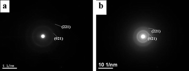
XRD patterns of the Sb2S3 nanowires obtained by ageing for 10 days are shown in Fig. 5b. All peaks may be indexed to an orthorhombic phase Sb2S3 (JCPDS files, no. 06-0474). The intensity of the (hk1) reflection peaks is enhanced, while that of the (hk0) planes such as (130) and (120) is absent or weakened, suggesting that the ultralong Sb2S3 nanowires might be preferentially elongated according to the [100] direction.7,8 The peak at 2 θ = 21.1° is likely to come from some impurities, and further experiments are under way to identify what the impurities are. The shape of the diffraction peaks indicate that the product obtained by ageing for 10 days is relatively well-crystallized to that prepared by 5 days of ageing. These are in good agreement with the electron diffraction (ED) patterns (Fig. 6a and b), which reveal clearer Debye–Scherrer rings due to the polycrystalline atomically more ordered structure for the sample with 10 days of ageing than that with 5 days of ageing.

According to Bashouti's report,15 the precursor molecules decomposed to form Sb2S3 upon a nucleophilic attack by the EDA solvent molecules, as shown schematically in Scheme 1.
 | ||
| Scheme 1 The formation of Sb2S3 from xanthate in EDA solution. | ||
The solvent EDA plays an important role in the formation and growth of Sb2S3 nanowires. When using ethanolamine (EA) as solvent, the decomposition reaction of (C2H5OCS2)3Sb occurred quickly. However, the yield of Sb2S3 was low and the length of the Sb2S3 nanowires was short (Fig. 7a). If ethylene glycol (EG), dimethyl sulfoxide (DMSO) or N,N-dimethylformamide (DMF) was used as solvent, no decomposition reaction took place in two days. As a bidentate ligand with two nitrogen donors, a stronger coordination interaction of EDA with Sb3+ may benefit the decomposition of xanthate, control the growth rate of different crystal faces and thus result in the formation of ultralong Sb2S3 nanowires. This synthetic route is also workable for the preparation of the other chalcogenides such as ZnS and PbS nanoparticles with well-defined nanostructures (Fig. 7b).
 | ||
| Fig. 7 TEM images of (a) Sb2S3 nanowires and (b) ZnS nanobelts and PbS cubes (inset) prepared by ageing for 5 days in EA and EDA solution, respectively. | ||
Fourier transform infrared (FTIR) studies of the as-prepared Sb2S3 also provide preliminary proof for the intermolecular bonding (Fig. 8). In comparison with the IR spectra of pure (C2H5OCSS)3Sb (Fig. 8a), the frequencies at 1190, 1105 and 1020 cm−1 attributed to the characteristic absorption for ν (C![[double bond, length as m-dash]](https://www.rsc.org/images/entities/char_e001.gif) S), ν (C–O–R), ν (C–S) of C2H5OCS2−group disappeared after reacting for 2 h (Fig. 8c), suggesting that the xanthate decomposed completely at room temperature in EDA solution. While, ν (C–N), ν (C–C), ν (CH2) and ν (NH2) signals at 1160, 1485 and 1608–1597 cm−1 in the IR data of free EDA (Fig. 8b) shift to 1400, 1518 and 1620 cm−1 in the case of Sb2S3 nanowires (Fig. 8c and d), respectively, which further demonstrates that the nitrogen atoms of the amine groups coordinated to the metal atom.
S), ν (C–O–R), ν (C–S) of C2H5OCS2−group disappeared after reacting for 2 h (Fig. 8c), suggesting that the xanthate decomposed completely at room temperature in EDA solution. While, ν (C–N), ν (C–C), ν (CH2) and ν (NH2) signals at 1160, 1485 and 1608–1597 cm−1 in the IR data of free EDA (Fig. 8b) shift to 1400, 1518 and 1620 cm−1 in the case of Sb2S3 nanowires (Fig. 8c and d), respectively, which further demonstrates that the nitrogen atoms of the amine groups coordinated to the metal atom.
 | ||
| Fig. 8 FTIR spectra of (a) (C2H5OCSS)3Sb, (b) EDA, (c) and (d) Sb2S3 prepared by ageing for 2 h and 10 days, respectively. | ||
Furthermore, Sb2S3 belongs to the orthorhombic system and forms a quasi-layered structure, which in itself has a strong preference for anisotropic growth, to form a 1D structure under certain conditions.6
The influence of pH and the concentration of the solution on the formation of Sb2S3 were investigated. The yield of Sb2S3 nanoparticles increased if some HCl was added into the solution, indicating that the decomposition rate of xanthate increased with decreasing pH, analogous to Sun's report.27 Nevertheless, the final morphology and structure of the products were the same. If the amount of the precursors (Sb xanthate) was decreased to 1.0 mmol in 20 mL of solution, the mixture sometimes changed color between clear yellow and turbid brown during ageing, suggesting that the decomposition reaction of xanthate might be reversible in EDA or EA solution at room temperature, and so the reaction rate increased with increasing concentration of the precursors.
The optical properties of the Sb2S3 nanowires have been studied by UV-vis reflectance spectroscopy. As shown in Fig. 9a, it can be found that Sb2S3 shows a strong photo-absorption property in the visible-light region and the absorption edge is as long as 750 nm. For a direct-gap semiconductor, the band gap of the as-prepared Sb2S3 nanowires is estimated at 1.63 eV using the formula [F(R)E]2 = A(E − Eg), where E and Eg are the photon energy and optical band gap energy, respectively, and A is the characteristic constant of semiconductors.21
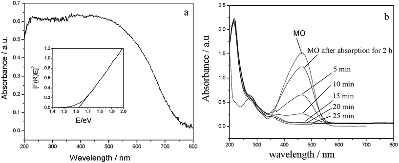 | ||
| Fig. 9 (a) UV-vis diffuse reflectance spectrum of the as-prepared Sb2S3 nanowires and its optical band gap energy Eg (inset); (b) UV-vis spectral changes of MO in aqueous Sb2S3 dispersions at various irradiation times. | ||
The photocatalytic activities of the as-prepared Sb2S3 nanowires are evaluated by decomposition of MO in aqueous solution under visible-light irradiation. The degradation course has been monitored by recording UV-vis absorbance spectra and following the decay of the main dye absorption peak at 464 nm. Fig. 9b shows that the as-prepared Sb2S3 nanowires were able to catalyze a complete decoloration after 25 min of irradiation, which is comparable to the degradation ratio of Sb2S3 nanorods determined by Sun's group.21 While, the degradation ratio of bulk Sb2S3 particles is about 7% (Fig. 10a), revealing that the photocatalytic activity is relative to particle size and surface area of the catalysts. In addition, the photocatalytic performance drops gradually for the Sb2S3 nanoparticles obtained by various ageing duration from 5 d to 6 h (Fig. 10), suggesting that the high crystallinity of a photocatalyst can effectively increase its photocatalytic activity.21
 | ||
| Fig. 10 Photocatalytic properties of different catalysts: (a) bulk Sb2S3 particles; Sb2S3 nanoparticles prepared after ageing for (b) 6 h, (c) 24 h, (d) 5 days, and (e) 10 days. | ||
Experimental
Syntheses
The experiments proceeded at room temperature and under atmospheric conditions. All chemicals were used as received without further purification. In a typical procedure, 1.1 g (0.005 mol) of SbCl3 was added into 60 mL of distilled water with stirring, and then about 4 mL of concentrated hydrochloric acid (HCl, 36%) was added dropwise to prevent the hydrolysis of SbCl3 and a homogeneous solution was obtained. 2.4 g (0.015 mol) of CH3CH2OCS2K was added into the above solution under agitation. Immediately, an orange precipitation ((C2H5OCS2)3Sb) was formed, and was collected after filtration, washed with deionized water several times and dried in air. Then, 0.8 g (about 1.6 mmol) of (C2H5OCS2)3Sb was dissolved in 20 mL of EDA, and the solution changed from clear yellow to turbid brown within several minutes. After the mixture was stirred for 10 days, brown Sb2S3 precipitates were collected by filtration, washed several times with water and absolute ethanol, and dried spontaneously in air.Characterizations
Transmission electron microscopy (TEM), high-resolution transmission electron microscopy (HRTEM) and the corresponding selected area electron diffraction (SAED) were carried out on a JEM-2100 microscope (JEOL) equipped with a METEK (PV 97-56700 ME) X-ray energy dispersive spectrometer. The specimens of TEM and HRTEM measurements were prepared via spreading a droplet of ethanol suspension onto a carbon-coated copper grid and allowing to dry in air. Raman spectra were collected on a RENISHAW InVia Raman microscope. The X-ray photoelectron spectra (XPS) were recorded on a PHI QUANTERA II X-ray photoelectron spectrometer, using Al Kα radiation as the exciting source. The results obtained in the XPS analysis were corrected by referencing the C 1s line to 284.6 eV. The X-ray diffraction patterns (XRD) were recorded on a Bruker D8 advanced X-ray diffractometer equipped with Cu-Kα radiation (λ = 1.5418 Å) in the range of 10–70°. The infrared spectroscopy on KBr pellets was performed on a Bruker Vector 22 spectrophotometer in the 4000–400 cm−1 region. The diffuse reflection spectra were measured on a Shimadzu UV-2550 spectrophotometer equipped with an integrating sphere, using BaSO4 as a reference.Photocatalytic activity test
The photocatalytic reaction was conducted in a reactor equipped with a 500 W Xe lamp and a 420 nm UV cut-off filter. A 200 mg quantity of photocatalyst was suspended in 200 mL of 10 mg L−1 MO aqueous solution. The suspension was ultrasonicated for 15 min and magnetically stirred in the dark for 2 h to ensure the establishment of an adsorption–desorption equilibrium of the dye on the catalyst surface. Then, the suspension was stirred and illuminated by visible light. At given time intervals, 5 mL of the suspension was taken out from the reactor and centrifuged to remove the photocatalyst particles. The concentration of MO during degradation was determined on a UV-vis spectrometer and estimated from the absorbance of the absorption maximum at 464 nm.Conclusions
In summary, we have used a room temperature crystallization process to produce Sb2S3 nanowires with a diameter in the range of 5–10 nm and length up to tens of micrometres from molecular precursors (xanthate) in EDA solution. This synthetic route is also workable for the preparation of belt-like ZnS and cubic PbS nanostructures. The as-prepared Sb2S3 nanowires with a direct band gap of 1.63 eV show high photocatalytic activity of MO degradation under visible-light irradiation. This work not only provides a facile route to synthesize chalcogenides with well-defined nanostructures at room temperature in a solution-phase system, but also gives insight into understanding the decomposition behavior of molecular precursors in various solvents.Acknowledgements
This work was financially supported by National Natural Science Foundation of China and NUST Research Funding (2010GJPY042).References
- P. Yang, R. Yan and M. Fardy, Nano Lett., 2010, 10, 1529–1536 CrossRef CAS.
- Y. Cui, Q. Wei, H. Park and C. M. Lieber, Science, 2001, 293, 1289–1292 CrossRef CAS.
- Y. Hu, H. O. H. Churchill, D. J. Reilly, J. Xiang, C. M. Lieber and C. M. Marcus, Nat. Nanotechnol., 2007, 2, 622–625 CrossRef CAS.
- P. J. Pauzauskie, D. J. Sirbuly and P. Yang, Phys. Rev. Lett., 2006, 96, 143903 CrossRef.
- E. Stern, J. F. Klemic, D. A. Routenberg, P. N. Wyrembak, D. B. Turner-Evans, A. D. Hamilton, D. A. LaVan, T. M. Fahmy and M. A. Reed, Nature, 2007, 445, 519–522 CrossRef CAS.
- Y. Yu, R. H. Wang, Q. Chen and L. M. Peng, J. Phys. Chem. B, 2005, 109, 23312–23315 CrossRef CAS.
- Z. R. Geng, M. X. Wang, G. H. Yue and P. X. Yan, J. Cryst. Growth, 2008, 310, 341–344 CrossRef CAS.
- X. Zheng, Y. Xie, L. Zhu, X. Jiang, Y. Jia, W. Song and Y. Sun, Inorg. Chem., 2002, 41, 455–461 CrossRef CAS.
- K. H. Park, J. Choi, H. J. Kim, J. B. Lee and S. U. Son, Chem. Mater., 2007, 19, 3861–3863 CrossRef CAS.
- J. Ota and S. K. Srivastava, Cryst. Growth Des., 2007, 7, 343–347 CrossRef CAS.
- P. Salinas-Estevané and E. M. Sánchez, Cryst. Growth Des., 2010, 10, 3917–3924 CrossRef CAS.
- R. J. Mehta, C. Karthik, W. Jiang, B. Singh, Y. Shi, R. W. Siegel, T. Theo Borca-Tasciuc and G. Ramanath, Nano Lett., 2010, 10, 4417–4422 CrossRef CAS.
- R. B. Yang, N. Zakharov, O. Moutanabbir, K. Scheerschmidt, L. M. Wu, U. Gösele, J. Bachmann and K. Nielsch, J. Am. Chem. Soc., 2010, 132, 7592–7594 CrossRef CAS.
- O. C. Monteiro, H. I. S. Nogueira and T. Trindade, Chem. Mater., 2001, 13, 2103–2111 CAS.
- M. Bashouti and E. Lifshitz, Inorg. Chem., 2008, 47, 678–682 CrossRef CAS.
- M. A. Malik, M. Afzaal and P. O'Brien, Chem. Rev., 2010, 110, 4417–4446 CrossRef CAS.
- C. An, K. Tang, Q. Yang and Y. Qian, Inorg. Chem., 2003, 42, 8081–8086 CrossRef CAS.
- Q. Han, J. Chen, X. Yang, L. Lu and X. Wang, J. Phys. Chem. C, 2007, 111, 14072–14077 CrossRef CAS.
- Q. Han, L. Chen, M. Wang, X. Yang, L. Lu and X. Wang, Mater. Sci. Eng., B, 2010, 166, 118–121 CrossRef CAS.
- A. L. Linsebigler, G. Lu and J. T. Yates, Chem. Rev., 1995, 95, 735–758 CrossRef CAS.
- M. Sun, D. Li, W. Li, Y. Chen, Z. Chen, Y. He and X. Fu, J. Phys. Chem. C, 2008, 112, 18076–18081 CrossRef CAS.
- K. Q. Li, F. Q. Huang and X. P. Lin, Scr. Mater., 2008, 58, 834–837 CrossRef CAS.
- B. Frumarová, M. Bílková, M. Frumar, M. Repka and J. Jedelský, J. Non-Cryst. Solids, 2003, 326–327, 348–352 CrossRef.
- J. Ota, P. Roy, S. K. Srivastava, B. B. Nayak and A. K. Arvind Kumar Saxena, Cryst. Growth Des., 2008, 8, 2019–2023 CrossRef CAS.
- X. Wang and Y. Li, Chem.–Eur. J., 2003, 9, 300–306 CrossRef CAS.
- X. Cao, L. Gu, W. Wang, W. Gao, L. Zhuge and Y. Li, J. Cryst. Growth, 2006, 286, 96–101 CrossRef CAS.
- Z. Sun and W. Forsling, Miner. Eng., 1997, 10, 389–400 CrossRef CAS.
| This journal is © The Royal Society of Chemistry 2011 |