Chemical reactions under autogenic pressure at elevated temperature to fabricate photo-luminescent Ga2O3 nanocrystals and their coatings
Pani P.
George
,
Vilas G.
Pol
*,
Yuri
Koltypin
,
Makluf Shirly
Ben-David
,
I.
Genish
and
Aharon
Gedanken
*
Institute for Nanotechnology and Advanced Materials, Bar-Ilan University, Ramat-gan, 52900, Israel. E-mail: vilaspol@gmail.com
First published on 1st September 2011
Abstract
Nanocrystalline (<20 nm) gallium oxide coating on in situ formed amorphous carbon spheres is achieved by the controlled chemical reaction of gallium triacetylacetonate under autogenic pressure at elevated temperature (700 °C) in an inert atmosphere. The as-prepared nanocomposite was further heated to 500 °C for 1 h in an air atmosphere to produce neat Ga2O3 nanocrystals. The room temperature photoluminescence (PL) measurements confirmed that the neat Ga2O3 nanocrystals exhibited enhanced PL intensity compared to Ga2O3 nanocrystals coated on carbon spheres. Moreover, the diverse ability of the autogenic process to coat pristine stainless steel plate with micron sized (<1 μm) Ga2O3 particles is demonstrated. This is a noteworthy advancement in the field of nanofabrication processes. The methodical morphological, compositional and structural characterizations of the products are carried out and plausible mechanistic elucidation of their formation is reported.
1. Introduction
During the past two decades, the fabrication of various fascinating nanostructures (e.g. nano-particles, rods, fibers, tubes, wires, plates) with the size in the order of Bohr exciton is of intense research interest due to their attractive physical and chemical properties. Eventually, new potential applications in nanodevices such as light emitting diodes, resonant tunnelling devices, lasers, catalysis, and gas sensors, etc. were developed.1 Therefore, considerable efforts have been made to synthesize many nano-material systems such as carbon, oxides, nitrides, borides, sulphides, carbides, and semiconductors. Specifically, Ga2O3 has wide range of applications such as transparent conducting oxide,2–3 an optical emitter for UV light,4 and high temperature gas sensors.5 Monoclinic gallium oxide (β-Ga2O3) is a wide band gap semiconductor material (Eg ≈ 4.9 eV),6 which also exhibits conduction.7Accordingly, a variety of synthetic techniques for the production of Ga2O3 particles with various morphologies is reported in the literature. For example, thermal oxidation,8 arc-discharge,9laser ablation,10,11 and carbothermal reduction12 are explored before. These synthetic methods require either a template or catalyst and most often occur at high temperatures. In this article, we report the RAPET (Reactions under Autogenic Pressure at Elevated Temperatures) approach for the fabrication of Ga2O3 nano or microstructures and their in situ or ex situ coatings on different surfaces. The literature shows that the RAPET technique is exceedingly successful at fabricating various captivating nanostructures of carbides, oxides, borides, nitrides, phosphides, sulfides, selenides, and carbonaceous materials.13 These materials are applicable in lithium-ion batteries as cathode or anode materials, optical and luminescent devices, hydrogen storage, superconducting and magnetic devices as well as acted as a catalyst supports.14–21 These chemical reactions are carried out in one-pot, without any solvents, above the dissociation temperatures of the chemical precursor(s) at elevated temperature in a closed reactor creating autogenic pressure. The pyrolyzed chemical precursor(s) in a closed system attain supercritical phases such as solid-liquid, solid-gas, liquid-gas, or gas-gas interactions.13 Those phases go through the nucleation and growth of individual components based on thermodynamic and kinetic stabilities of the precursor components, usually yielding materials in nanodimensions. The as-obtained dry powders are usually pure, thus do not involve any intricate chemical processing or handling for cleansing the obtained materials.
However, none of the previous RAPET literature demonstrated the efforts on the synthesis of luminescent Ga2O3 nanoparticles or its coating of pristine pieces of metal (such as stainless steel). In this paper, we report the independent chemical dry reactions using gallium triacetylacetonate precursor under RAPET conditions in an inert atmosphere for the synthesis of Ga2O3 crystals and in situ coating on various surfaces.
2. Experimental
The synthesis of nanocrystalline gallium oxide coating on in situ formed amorphous carbon spheres is carried out by the thermal dissociation of gallium triacetylacetonate, Ga(acac)3, which was purchased from Aldrich, and used as received. In a typical synthesis, 1 g of Ga(acac)3 was introduced into the specially designed, ventable 5 cm3 reactor at room temperature under inert atmosphere and closed. The temperature of the partially filled reactor was raised at a heating rate of 10 °C min−1 to 700 °C, and held for 3 h. The chemical reaction(s) took place within the elements (Ga, O, H, and C) present in the Ga(acac)3 precursor under the autogenic pressure conditions. After 3 h, the reactor was naturally cooled to room temperature, and opened; 0.69 g (69% total yield) black powder was obtained. The yield is defined as the final weight of the product relative to the weight of Ga(acac)3, the starting material. The as-prepared dry product is characterized as nanocrystalline gallium oxide coated on in situ formed amorphous carbon spheres (Ga2O3–carbon). The as-prepared Ga2O3–carbon nanocrystals were further heated to 500 °C under air for 1 h to remove carbon in a ventilating hood, yielding white colored Ga2O3 nanocrystals (Ga2O3).In an analogous controlled experiment, 1 g of the Ga(acac)3 was introduced into the reactor along with the two small, clean stainless steel plates (SSP). The analogous reaction conditions were employed as described above. Surprisingly, it is pragmatic that less than one micrometre diameter Ga2O3 particles and some carbon spheres decorated the surface of pristine stainless steel plate, demonstrating the assorted ability of the RAPET process.
2.2. Characterization
The XRD patterns of various samples were recorded using a Bruker D8 diffractometer with Cu-Kα radiation. The C, H analysis was carried out on an Eager 200 CE instrument and an EA 1110 Elemental Analyzer. The morphologies of the as-prepared sample, and also of the heated product were studied by a scanning electron microscope (SEM) coupled with energy dispersive X-ray (EDX) analysis. Transmission electron microscopy (TEM) studies were carried out on a JEOL 2000 electron microscope. High-resolution TEM (HRTEM) images were taken using a JEOL 2010 with 200 kV accelerating voltage. Samples for the TEM and HRTEM measurements were obtained by placing a drop of the suspension from the as-sonicated reaction product in ethanol onto a carbon-coated copper grid, followed by drying in air to remove the solvent. The optical absorption spectra were measured on a Shimadzu UV-2100 spectrophotometer at room temperature. The photoluminescence measurements were performed on a Perkin Elmer Luminescence spectrometer L550B at room temperature.3. Results and discussion
3.1. Powder X-ray diffraction (PXRD) and elemental (C and H) analysis
The PXRD patterns of the Ga2O3 coated on carbon composite and Ga2O3 nanocrystal samples are depicted in Fig. 1a and 1b, respectively. The main diffraction peaks are indexed undisputably to the monoclinic structure of Ga2O3.22 The absence of graphite peaks indicates the possibility that carbon is present only as in the amorphous form. This is due to unfavorable reaction conditions for the graphitic growth in the presence of Ga2O3 particles. To achieve carbon free Ga2O3 crystals, Ga2O3–carbon composite was further heated to 500 °C for 1 h in an air atmosphere. The similar diffraction peaks, peak intensities, and cell parameters are recorded in agreement with the diffraction peaks of the crystalline monoclinic structure of Ga2O3. The recorded diffraction pattern of Ga2O3 nanocrystals is equivalent to that of the Ga2O3–carbon composite, verifying that no structural alteration occurred during the combustion. | ||
| Fig. 1 PXRD pattern of (a) nanocrystalline Ga2O3 coated on carbon spheres and (b) neat Ga2O3 nanocrystals. | ||
The chemical element contents in the precursor, Ga(acac)3 is theoretically calculated and compared with the recorded values in the prepared Ga2O3–carbon composite. The calculated elemental (wt) percentages of C, H, O and Ga in the Ga(acac)3 precursor are 49.0%, 5.7%, 26.1%, and 19.0%, respectively. The employed C, H, N and S elemental analyzer determined the averaged 43 wt% of carbon and around 0.5 wt% of hydrogen content in the Ga2O3–carbon composite. It is clear that some amount of carbon and hydrogen in the Ga2O3–carbon composite is reduced, as compared to the precursor, liberating CO2, CxHy (hydrocarbons) and/or H2 gases during the controlled thermolysis of the precursor.23 It is further confirmed by C, H, N, S analysis that almost all the hydrogen and carbon contents has been removed from the heated Ga2O3 sample.
3.2 Morphology
The overall morphologies of the Ga2O3–carbon composite and the Ga2O3 nanocrystals obtained after annealing at 500 °C under air atmosphere are primarily investigated by SEM measurements. SEM image of the Ga2O3–carbon composite (Fig. 2a) illustrates mostly the 1–4 μm spherical carbon particles. As determined above (by C, H, N, S analysis), indeed the high carbon contents are observed in the SEM. The coated small nanocrystalline Ga2O3 particles are not well resolved in the SEM, thus supplementary TEM analysis are carried out and the resolved images are provided in the following section. In 2005, Noble laureate Harold Kroto and his group reported the production of less than 1 μm carbon spheres via a direct flow pyrolysis of a wide range of hydrocarbons, including styrene, toluene, benzene, hexane, cyclohexane and ethene, in the absence of catalyst.24 However, in our experiments, the main origin for the formation of carbon spheres comes from the acetylacetonate present in the precursor. In addition, in ref. 24 it is demonstrated that inter-particle collisions are favorable and it results in the further growth of the small particles, when the experiments are conducted in a closed system. | ||
| Fig. 2 (a) SEM image of Ga2O3–carbon composite, (b) SEM image of neat Ga2O3 nanocrystals. | ||
Fig. 2b demonstrates the SEM images of the neat Ga2O3 nanocrystals obtained after the combustion of Ga2O3–carbon composite. The average diameter of secondary 100 nm particles comprising aggregated Ga2O3 nanocrystals is perceptible. The absence of any carbon spheres confirmed its absolute removal during combustion of Ga2O3–carbon composite.
3.3. TEM and HRTEM measurements
The detailed morphology and structure of the RAPET produced Ga2O3–carbon composite and converted Ga2O3 nanocrystals were further studied by TEM and HRTEM measurements. Fig. 3a–b demonstrated that 2–4 μm carbon spheres are in situ coated with Ga2O3 nanoparticles during the controlled thermal decomposition of Ga(acac)3 at 700 °C. Around 15 nm Ga2O3 nanocrystals are non-uniformly coated on the surface of carbon spheres. The Ga2O3 nanoparticles synthesized by employing the RAPET technique exhibit a spherical shape, which differs from the rod-shaped Ga2O3 nanoparticles obtained by Lin et al.25 Lin's synthetic strategy is a hydrothermal technique and the reaction was conducted for approximately 30 h to obtain amorphous Ga2O3 and requires one more heating step (900 °C in air) for attaining 270 nm diameter Ga2O3 crystals. In contrast, both the materials made by RAPET are highly crystalline, prepared from single Ga(acac)3 precursor, without solvents. Fig. 3c shows the HRTEM image of the edge of the nanocrystalline Ga2O3 particles supported on carbon spheres. The obtained inserted diffuse ring pattern, further confirms that mostly the supported carbon spheres are amorphous. These results correspond to the XRD measurements. | ||
| Fig. 3 (a–b) Transmission electron micrographs of Ga2O3–carbon composite at different magnifications, and (c) HR-TEM, and electron diffraction on carbon spheres. | ||
To accomplish the comprehensive morphological and structural understanding of Ga2O3 nanocrystals, energy dispersive X-ray spectroscopy (EDS), TEM, HR-TEM and electron diffraction analysis were carried out. Fig. 4a shows the TEM image and EDS of the neat Ga2O3 nanocrystals. The neat Ga2O3 nanocrystals have diameters between 10–20 nm. The obtained EDS spectrum demonstrates the existence of Ga, O from the sample and the Cu originated from the supported TEM grid. No other impurities were found in the EDS measurement, confirming the high purity of the RAPET achieved product. Fig. 4b represents the HRTEM image of Ga2O3 nanocrystals with the interlayer spacing of 0.298 for the (400) plane of the Ga2O3 nanoparticle. The measured distance between these (400) lattice planes is very close to the distance between the planes reported in the literature (0.298 nm) for the monoclinic lattice of gallium oxide (PDF: 00-041-1103). The obtained sharp diffraction ring pattern exhibit the crystalline nature of the Ga2O3.
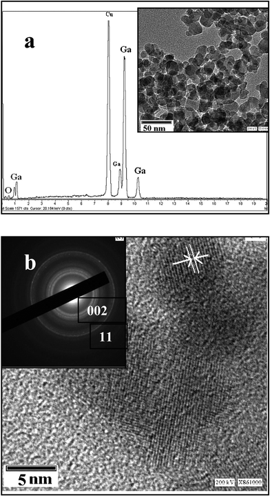 | ||
| Fig. 4 (a) EDS and TEM of Ga2O3 nanocrystals, (b) HRTEM and electron diffraction (ED) pattern of Ga2O3 nanocrystals. | ||
3.4 Optical properties of Ga2O3–carbon nanocomposite and Ga2O3 nanocrystals
Considering the important applications of monoclinic β-Ga2O3 as an optical emitter, gas sensor and also transparent conducting oxide, the optical (UV-Vis spectra and photoluminescence) properties were studied. In the UV-Vis measurements, the samples were dispersed in ethanol and ethanol was also used as a reference. Fig. 5a shows the typical UV-Vis spectra of the nanocrystalline Ga2O3 and Ga2O3–carbon composite. An estimate of the optical band gap is obtained using the following equation for a semiconductor.26| α(ν) = A(ħν/2 – Eg)m/2 |
 | ||
| Fig. 5 (a) Room temperature UV-vis absorption spectrum of Ga2O3–carbon composite and Ga2O3 nanocrystals. (b) The photoluminescence spectra of Ga2O3–carbon composite and Ga2O3 nanocrystals. | ||
The photo-luminescence (PL) spectra of the Ga2O3–carbon composite and Ga2O3 nanocrystals were measured on F-850 fluorescence spectrophotometer (Hitachi) using an excitation wavelength of 325 nm at room temperature. Fig. 5b shows a strong and broad PL emission spectrum recorded for the Ga2O3 nanocrystals. The emission is mainly located in the blue-green region with fluorescence peak centered at 468 nm. In contrast, the composite Ga2O3–carbon has a weak emission band with peak located at 465 nm. This emission peak is related to the different energy levels produced by the oxygen vacancies. We anticipate that carbon spheres coated with the Ga2O3 nanoparticles inhibit the Ga2O3 nanocrystals from absorbing the UV radiation. The emission at 468 and 465 nm for neat Ga2O3 and Ga2O3–carbon composite respectively indicates a slight blue shift of 7–10 nm compared with the PL peak of Ga2O3 powder. The slight blue shifts can be attributed to the nanoparticle size effect. Lin et al. demonstrated the photoluminescence measurements of Ga2O3 nanorods and observed the broad emission band ranging from 300–600 nm,28 which is attributed to the recombination of an electron on an oxygen donor with a hole formed by gallium acceptor.
The powder XRD of the as prepared sample obtained after the RAPET reaction confirmed the presence of Ga2O3. The absence of other impurities like GaOOH in the final product at the end elucidates that all the amount of starting material is utilized in producing the gallium metal oxide nanocrystals. Under the RAPET reaction conditions, Ga(acac)3 decomposes into the gaseous C, H and small nuclei of Ga2O3. Yang et al. and Xiag et al. synthesized the Ga2O3 nanostructures by evaporating the metallic Ga in the flow of argon, by raising the temperature to 900 and 950 °C respectively.29,30 The occurrence of metal oxide nanoparticles by RAPET reaction of metal alkoxides and metal acetates were earlier demonstrated by us in a series of papers.31–33 In the literature, reduced Ga gas phase species and thermally stable Ga(I) or Ga(III)-hydride intermediates phases34 are reported. In the present case, thermally dissociated chemical species are held in a critical phase in an enclosed system, allowing the carbon spheres to nucleate before the Ga species. Based on thermodynamic arguments, i.e. melting point of carbon is higher than that of transition metal oxides, carbon spheres are formed first and Ga2O3 nanocrystals are formed on the carbon surface.
In a control experiment, the successful growth of micron sized Ga2O3 crystals on the stainless steel plate (SSP) is carried out by the thermal decomposition of Ga(acac)3 in the presence of the SSP in the closed reactor at elevated temperature (700 °C/3 h) under autogenic pressure. The morphologies of the Ga2O3 particles at SSP are primarily investigated by SEM measurements. Fig. 6a represents the flat SSP before starting the reaction, confirming the smooth and clean surface. The SEM image of the as coated SSP is shown in Fig. 6b, evidence that the SSP is coated with micron sized Ga2O3 crystals and carbon spheres. Fig. 3c is a higher magnification image of grown multi-faceted Ga2O3 micro crystals on the SSP surface. The average diameter of Ga2O3 crystal is 1 μm, which is contrary to the 15 nm Ga2O3 nanocrystals prepared without SSP. The growth of Ga2O3 microcrystals on the surface of the SSP is explained as follows. In this reaction, the SSP placed along with the Ga(acac)3 precursor inside the reactor, was heated to 700 °C for 3 h. The gap between the dissociated Ga(acac)3 moieties and stainless steel plate got supersaturated because of its confinement inside the close reactor. The vapor condensation, nucleation and growth of the Ga2O3 particles can occur on the SSP surface, resulted into micrometre size structures. The XRD pattern of the Ga2O3 microcrystals grown on SSP showed sharper reflection lines than the Ga2O3–carbon composite. The sharper peaks reflected on the bigger particle dimensions. Jung et al. obtained Ga2O3 microplates35 on sapphire by thermal treatment of compacted GaN powder under an argon flow. The Ga2O3 nanocrystals can be used in opto-electric devices operating in the near UV-near IR spectral region.
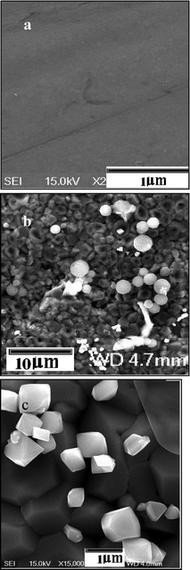 | ||
| Fig. 6 (a) SEM image of the plain stainless steel plate (SSP), (b) SEM image of the SSP coated with micro crystals of Ga2O3 with the carbon spheres, and (c) SEM image of micron sized Ga2O3 multifaceted particles deposited on the SSP. | ||
Conclusions
This paper demonstrated the fabrication of luminescent Ga2O3 nanoparticles coated on carbon spheres viaRAPET technique and its combustion to bare Ga2O3 nanocrystals. The measured room temperature photoluminescence intensity of the neat Ga2O3 nanocrystals is higher compared to Ga2O3 nanocrystals coated on carbon spheres. The systematic morphological, compositional and structural analysis of all the products elucidated the plausible reaction mechanism of their formation. It is also revealed that RAPET is an effective technique for in situ coating of the Ga2O3 multifaceted crystals on the stainless steel plates, without using any catalyst.Acknowledgements
We thank the Bar-Ilan Research authority for providing us with the scientific instrumental facilities to carry out this work.References
- S. Sharma and M. K. Sunkara, J. Am. Chem. Soc., 2002, 124, 12288 CrossRef CAS.
- M. C. Daniel and D. Astruc, Chem. Rev., 2004, 104(1), 293 CrossRef CAS.
- D. D. Edwards, T. O. Mason, F. Goutenoire and K. R. Poeppelmeier, Appl. Phys. Lett., 1997, 70, 1706 CrossRef CAS.
- L. Binet and D. Gourier, J. Phys. Chem. Solids, 1998, 59, 1241 CrossRef CAS.
- M. Ogita, N. Saika, Y. Nakanishi and Y. Hatanaka, Appl. Surf. Sci., 1999, 142, 188 CrossRef CAS.
- K-W Chang and J-J Wu, Adv. Mater., 2004, 16, 545 CrossRef CAS.
- M. R. Lorenz, J. F. Woods and R. J. Gambino, J. Phys. Chem. Solids, 1967, 28, 403 CrossRef CAS.
- J. Y. Li, Z. Y. Qiao, X. L. Chen, Y. G. Cao, M. He, H. Li, Z. M. Cao and Z. Zhang, J. Alloys Compd., 2000, 306, 300 CrossRef CAS.
- W. Q. Han, P. Kohler-Redlich, F. Ernst and M. Rühle, Solid State Commun., 2000, 115, 527 CrossRef CAS.
- J. K. Hu, Q. Li, X. M. Meng, C. S. Lee, D. J. Bae, Y. H. Lee, G. Park, W. B. Choi and N. S. Kim, Adv. Mater., 2000, 12, 746 CrossRef.
- C. M. Lieber, Solid State Commun., 1998, 107, 607 CrossRef CAS.
- R. Ma and Y. Bando, Chem. Phys. Lett., 2003, 367, 219 CrossRef CAS.
- V. G. Pol, S. V. Pol and A. Gedanken, Adv. Mater., 2011, 23, 1179 CrossRef CAS.
- S. V. Pol, V. G. Pol and A. Gedanken, J. Phys. Chem. C, 2007, 111, 16781 CAS 12.
- A. Odani, V. G. Pol, S. V. Pol, M. Koltypin, A. Gedanken and D. Aurbach, Adv. Mater., 2006, 18, 1431 CrossRef CAS.
- V. G. Pol, J. M. Calderon-Moreno and P. Thiyagarajan, Langmuir, 2008, 24, 13640 CrossRef CAS.
- V. G. Pol, S. V. Pol, A. Gedanken, S. H. Lim, Z. Zhong and J. Lin, J. Phys. Chem. B, 2006, 110, 11237 CrossRef CAS.
- V. G. Pol, S. V. Pol and A. Gedanken, Carbon: Sci. Technol., 2008, 1, 46 CAS.
- S. V. Pol, V. G. Pol and A. Gedanken, J. Phys. Chem. C, 2007, 111, 16781 CAS.
- S. Shanmugam and A. Gedanken, Small, 2007, 3, 1189 CrossRef CAS.
- S. V. Pol, V. G. Pol and A. Gedanken, Chem.–Eur. J., 2004, 10, 4467 CrossRef CAS.
- L. Jianye, C. Xiaolong, Q. Zhiyu, H. Meng and L. Hui, J. Phys.: Condens. Matter, 2001, 13, L937–L941 CrossRef.
- P. P. George, V. G. Pol and A. Gedanken, Nanoscale Res. Lett., 2007, 2, 17–23 CrossRef CAS.
- Z. J. Yi, G. Chao, K. H. Wen, Z. Yanqiu, H. Andrzej, B. Michal, R. Martin, Y. L. Chi, A. Steve, H. Kroto and R. M. V. David, Carbon, 2005, 43, 1944 CrossRef.
- J. Zhang, Z. Liu, C. Lin and J. Lin, J. Cryst. Growth, 2005, 280, 99 CrossRef CAS.
- V. Luca, S. Djajanti and R. F. Howe, J. Phys. Chem. B, 1998, 102, 10650 CrossRef CAS.
- C-L. Kuo and M. H. Huang, Nanotechnology, 2008, 19, 155604 CrossRef.
- J. Zhang, Z. Liu, C. Lin and J. Lin, J. Cryst. Growth, 2005, 280, 99–106 CrossRef CAS.
- Z. X. Yang, F. Zhu, W. M. Zhou and Y. F. Zhang, Phys. E., 2005, 30, 93 CrossRef CAS.
- X. Xiang, C-B. Cao, Y-J. Guo and H-S. Zhu, Chem. Phys. Lett., 2003, 378, 660 CrossRef CAS.
- S. V. Pol, V. G. Pol, I. Felner and A. Gedanken, Eur. J. Inorg. Chem., 2007, 2089–2096 CrossRef CAS.
- P. P George and A. Gedanken, Eur. J. Inorg. Chem., 2007, 6, 919–924 Search PubMed.
- P. P. George, A. Gedanken and A. Gabashvili, Mater. Res. Bull., 2007, 42, 626–632 CrossRef CAS.
- E. V. Suslova, V. G. Kessler, S. Gohil and N. Y. Turova, Eur. J. Inorg. Chem., 2007, 5182 CrossRef CAS.
- W. S. Jung, H. U. Joo and B. K. Min, Physica E, 2007, 36, 226 CrossRef CAS.
| This journal is © The Royal Society of Chemistry 2011 |