Tin oxide nanocrystals: controllable synthesis, characterization, optical properties and mechanistic insights into the formation process
Anshu
Singhal
*a,
Bhaskar
Sanyal
b and
Avesh K.
Tyagi
a
aChemistry Division, Bhabha Atomic Research Centre, Mumbai, 400 085, India
bFood Technology Division, Bhabha Atomic Research Centre, Mumbai, 400 085, India. E-mail: anshus@barc.gov.in; Fax: 91 22 2550 5151; Tel: 91 22 2559 2235
First published on 12th September 2011
Abstract
A novel, surfactant-free, solution-phase method has been successfully developed for the synthesis of SnO2 nanocrystals using a solvothermal route. The nanocrystals having average diameters in the range 4–8 nm, have been synthesized by a non-aqueous sol–gel reaction using tin(IV) bis(acetylacetonate)dichloride, [(Sn(acac)2Cl2)] with benzyl alcohol as the reaction medium at 200 °C. The crystal structure, morphology, and sizes of the SnO2 nanocrystals have been determined by X-ray diffraction (XRD), transmission electron microscopy (TEM) and Raman studies. Raman peaks at 627, 768 cm−1 characteristic of the rutile phase of bulk SnO2 are observed along with broad surface vibration modes in the range 400–600 cm−1. Optical properties of the nanocrystals have been explored by optical absorption and photoluminescence (PL). A blue shift of the optical band gap of the nanocrystals is observed due to size effects. The estimated band gap of the SnO2 nanocrystals from optical absorption data is found to be 3.81 eV. The photoluminescence spectrum showed broad UV as well as visible emission. Based on the GC-MS and carbon-13 NMR analysis of the final reaction solution, a formation mechanism encompassing the ether elimination and solvolysis of acetylacetonate ligand is proposed.
1. Introduction
Multifunctional materials of reduced dimensionality have become an increasingly active area of research in chemistry and physics at the nanoscale. On the nanoscale, physical and chemical properties of nanomaterials, and hence their further applications depend not only on the composition but also on the particle size and shape.1 In recent years, semiconducting metal oxide nanostructures have been extensively studied in view of their potential applications as photocatalysts, battery materials, sensors, and optoelectronic devices because of their quantum confinement effect and size- and shape-dependent characteristics.2–5Tin oxide (SnO2) is an n-type wide band gap (Eg = 3.6 eV) semiconductor and due to its unique electrical, optical, and electrochemical properties, offers wide range of potential technological applications in gas sensing,4 transparent conducting electrodes,6 electrochemical devices7 and dye based solar cells.8 Thus, the synthesis of SnO2 nanostructures with high crystallinity and well-defined particle morphologies with narrow-size distribution is of great technological and scientific interest.Several literature reports on physical synthetic methods of this material are available9 but these usually involve high temperature and complex procedures. A variety of chemical methods, viz., solution route,10,11 sol–gel,12 hydrothermal,13 sonochemical,14 organometallic precursor synthesis,15 microwave synthesis,16,17 and surfactant mediated-method,18 have been used to prepare SnO2 nanoparticles. In some cases further annealing of as prepared samples is required to get crystalline products. In other cases, SnO2 nanoparticles prepared have diameters larger than that required for the emergence of quantum confinement effect (the exciton Bohr radius of SnO2 is only 2.7 nm). This limits their applications, to some extent. Further, some of the methods require use of surfactant to control the crystal growth and the surface functionalisation may influence the toxicity of the nanoparticles.19 Thus, the development of simple, mild surfactant free, and economical routes for the large scale synthesis of well-controlled SnO2 nanostructures still remains a challenge.
In the present work, we demonstrate a simple one pot economical route for the large-scale synthesis of highly crystalline SnO2 nanoparticles with average diameters in the range 4 to 8 nm via a solvothermal synthetic route using tin(IV) bis(acetylacetonate)dichloride with benzyl alcohol as the reaction medium without using any surfactant. The detailed structural characterization of the nanocrystals, their optical properties and mechanistic insights into their formation are also reported.
2. Experimental details
2.1 Materials
Tin(IV) bis(acetylacetonate)dichloride (98%, Aldrich), and anhydrous benzyl alcohol (99.8%, Aldrich) were used as received.2.2 Synthesis of SnO2 nanocrystals
SnO2 nanoparticles were synthesized by a nonhydrolytic sol–gel process in benzyl alcohol. In a typical preparation, tin(IV) bis(acetylacetonate)dichloride (0.5 g, 1.29 mmol) was dissolved in 40 ml of benzyl alcohol. After vigorously stirring for 15 min, the colorless solution was transferred to a Teflon cup in a stainless-steel-lined autoclave. The autoclave was maintained at 200 °C for 24 h and then was allowed to cool to room temperature. The resulting white product (% yield = 0.178 g, 91%) was retrieved by centrifugation and washed several times with toluene and then methanol to remove any starting material and finally vacuum dried at room temperature for 4 h.2.3 Characterization
The phase purity and structure of the nanocrystals were determined by X-ray powder diffraction data, which were collected on a Philips X'Pert pro X-ray diffractometer using monochromatized Cu Kα radiation (λ = 1.5418 Å) and operating at 40 kV and 30 mA. Low- and high–resolution (HR) transmission electron micrographs (TEM) were obtained using a FEI-Tecnai G-20 microscope operating at 200 kV. The TEM specimens were prepared by dispersing the samples in ethanol, and placing a drop of the dispersion on a copper TEM grid covered with a holey carbon film, which was then dried. Micro-Raman spectra of the nanocrystals were obtained on a Horiba Jobin Yvon Labram-HR make spectrometer using an Ar ion laser (514.5 nm). The absorption spectrum was recorded on a UV-visible spectrometer (JASCO model V-530 spectrophotometer). Photoluminescence measurements were carried out at room temperature using Edinburgh Instruments' FLSP 920 system having a 450 W xenon lamp as the excitation source. Electron paramagnetic resonance (EPR) spectra were recorded using EMX model EPR spectrometer (Bruker, Germany) operating at 9.42 GHz. The modulation frequency used was 100 KHz. Diphenyl picrylhydrazyl (DPPH) radical was used as reference for the calibration of g factor.N2-Brunauer-Emmett-Teller surface areas were measured with Quantachrome Autosorb-1 analyzer using nitrogen as the adsorbing gas. The reaction mechanisms were investigated by retro-analysis by using reaction solutions obtained after the removal of particulate products by centrifugation and filtration. GC-MS analysis was carried out on a Shimadzu GC–MS instrument (model GC-MS QP 2010) provided with an AB-1 capillary column. The peaks were identified by comparing their mass fragmentation pattern with the data available in the spectral library (Wiley/NIST Libraries, Shimadzu Corporation, Kyoto, Japan) of the instrument.13C{1H} spectra for the yellow organic and colorless phase were recorded in CDCl3 and D2O respectively, either on a Bruker Avance II 300 MHz or Varian mercury plus 300 spectrometer operating at 75.4 MHz. Chemical shifts are referenced to the internal chloroform peak for data in CDCl3 and external DSS (2, 2-dimethyl-2-silapentane-3,3,4,4,5,5-d6-5-sulfonate sodium salt) for data in D2O.
3 Results and discussion
3.1 Morphology and structure
The structure and morphology of the SnO2 nanoparticles were investigated by TEM. The representative low resolution image shown in Fig. 1a, illustrates that the nanocrystals are quite uniform in morphology. The shape is nearly spherical and the average diameter of the particles is in the range 4–8 nm. Although the particles are slightly agglomerated, because of lack of stabilizing surfactants, the grain boundaries are clearly distinguishable. The high crystallinity of the particles is further confirmed by selected area electron diffraction (SAED) and high-resolution (HR) TEM investigations. The SAED pattern of the nanoparticles is consistent with the tetragonal rutile structure of SnO2 featuring strong ring patterns assigned to (110), (101), (200), (211) and (112) planes (Fig. 1b). The HRTEM image, Fig. 1c, demonstrates the single crystal nature of the SnO2 nanocrystals. The lattice spacing of 0.338 nm between adjacent lattice planes in the image corresponds to the distance between two (110) crystal planes. | ||
| Fig. 1 (a) Low-resolution TEM image of SnO2 nanocrystals (b) SAED pattern and (c) HRTEM image of a single SnO2 nanocrystal (d) XRD pattern of SnO2 nanocrystals. | ||
The powder XRD pattern of the as-synthesized SnO2 nanocrystals sample is shown in Fig. 1d. The diffraction peaks reveal that the SnO2 nanocrystals have a tetragonal crystal structure with lattice parameters a = b = 4.737(1) Å and c = 3.185 Å, which are well matched with those of the corresponding bulk rutile SnO2 (P42/mnm, a = b = 4.7382 Å and c = 3.1871 Å, JPCDS No. 41-1445), while peaks are obviously broadened with decreasing crystal size. No other crystalline impurities were detected in the as synthesized product. The Brunauer-Emmett-Teller (BET) result indicates that the specific area of the SnO2 nanoparticles is 102 m2g−1. Consequently, from the results of the TEM, XRD, and BET analyses, the as-synthesized product could be determined to be pure rutile phase SnO2 with high specific area.
3.2 Raman studies
Raman scattering is a useful tool for the characterization of nanosized materials and a qualitative probe of the presence of lattice defects in solids.20SnO2 has a tetragonal rutile structure with space group P42/mnm. Group theory shows that in the first Brillouin zone there are four Raman active modes, i.e., B1g, Eg,,A1g, and B2g.21 The infrared (IR) active modes are A2u and Eu. Fig. 2 shows the Raman spectrum of as-synthesized SnO2 nanocrystals. The fundamental Raman peaks at 627 and 768 cm−1 corresponding to A1g and B2g vibration modes, respectively are observed, in good agreement with those for rutile bulk SnO2.21 However, the Raman peaks of the present SnO2 nanoparticles are broad and slightly shifted to lower wave numbers as compared to bulk rutile SnO2. This can be understood as coming from size effects. Fauchet et al.22 reported that while Si nanocrystals are smaller than 30 nm, it would lead to down shift and broadening of the Raman spectrum. In addition to the fundamental Raman peaks, a broad peak at 307 cm−1 and a very broad band located in the range 400–600 cm−1 is observed, these peaks are not observed in bulk rutile SnO2. The broad band located between 400–600 cm−1 is attributed to the surface vibration modes.23 The origin of band/peak at 307 cm−1 is not yet fully elucidated. In earlier studies, Sun et al.,24 and Rumyantseva et al.25 have reported similar results for rutile SnO2 nanobelts and SnO2 nanocrystalline powders respectively. Sun et al. observed a weak band at 313 cm−1 in the rutile SnO2 nanobelts, whereas, Rumyantseva et al. observed Raman bands at 310–350 cm−1 for SnO2 nanocrystalline powders. Abello et al.23 proposed that the relaxation of the k = 0 selection rule is progressive when the rate of disorder increases or the size decreases. Thus in case of nanostructures with reduced dimension, some infrared (IR) modes may become weakly active when the structural changes induced by disorder and size effects take place. Therefore, this band could be due to an active mode from the inactive Eu mode in bulk material.23 The observance of Raman band in the region 310–350 cm−1, in SnO2 nanocrystals prepared by us and other groups seems to strengthen the association of this band with the effects due to the nanostructure size against those due to the synthesis procedure. The Raman spectrum confirms the characteristics of the tetragonal rutile structure as well as the very small size of the SnO2 nanocrystals.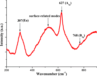 | ||
| Fig. 2 Room temperature micro-Raman spectrum of SnO2 nanocrystals. | ||
3.3 Optical properties
High-energy shift of an absorption edge is generally expected for semiconductor nanoparticles. To confirm this, the absorption spectrum was acquired from the SnO2 nanoparticles and the results are shown in Fig. 3. The value of the absorption onset of the nanoparticles is found to be ∼300 nm. The optical absorption coefficient α of a semiconductor close to the band edge can be expressed by the following equation:| α = K(hυ-Eg)n/hυ |
 | ||
| Fig. 3 Optical absorption spectra of SnO2 nanocrystals recorded at room temperature. | ||
where K is a constant, Eg is the band gap, and n is a value that depends on the nature of the transition. The optical transition of SnO2 is known to be a direct type.26 (In this case, n is equal to 1/2 for this direct allowed transition. The band gap can be estimated from a plot of (αhυ)2versusphoton energy. Plots of (α (hν))2versus hν can be derived from the absorption data in Fig. 4. The intercept of the tangents to the plot gives a good approximation of the band gap energy of the direct band gap materials. The band gap of the SnO2 nanocrystals (3.81 eV) is larger than the value of 3.62 eV for the bulk SnO2 (inset Fig. 3).
 | ||
| Fig. 4 (a) Room temperature PL spectrum for SnO2 nanocrystals (λexc = 240 nm). (b) Pictorial representation showing the defect state emission from SnO2 nanocrystals. (c) EPR spectrum of SnO2 nanocrystals recorded at room temperature. | ||
Photoluminescence (PL) is a very useful tool to determine the structure, defect, and impurity in the nanocrystals. Literature studies on PL of SnO2 nanocrystals reveal that luminescence is generally observed both in UV and visible region (range 350–550 nm).27,28 We also observe UV and visible emission for the SnO2 nanocrystals prepared in the present study. Fig. 4a shows the photoluminescence spectrum of SnO2 nanoparticles recorded at room temperature. The peaks are observed at 369.24 nm (3.36 eV), 380.7 nm (3.26 eV), 393.82 nm (3.15 eV), 418.41 nm (2.96 eV), 450.36 nm (2.75 eV), 480.68 nm (2.58 eV), 490.51 nm (2.53 eV) and 557.70 nm (2.22 eV). The broad peak at 3.36 eV can be assigned as the recombination of band to acceptor and donor to acceptor and has been previously observed both for bulk SnO229 and SnO2 nanowires.30 The luminescence in the visible region is generally believed to come from defects such as oxygen vacancies, tin interstitial or dangling bonds.31−33 In general, oxygen vacancy is known to be the most common defect in nanocrystalline oxides,32,33 and usually acts as the radiative center in the luminescence process by forming defect levels located inside the gap and trapping electrons from the valence band. The detailed mechanism for the defect PL is depicted pictorially in Fig. 4b. After the excitation of electrons to a highly excited state in the conduction band, the carriers relax to the band edge. Some carriers can be trapped by the shallow defects in the band gap. They either recombine with holes in the valence band or continue to relax to deeper defect states before recombining. The broad emissions observed in visible wavelength range for the SnO2 nanocrystals prepared are interpreted by this mechanism. The oxygen vacancies can be present in three different charge states in the oxides: V0O, V+O, and V++O states. Only the V+O state is paramagnetic, and consequently observable by EPR. As V0O is assumed to be a shallow donor,34 it is expected that most oxygen vacancies will be in their paramagnetic V+O states under the flat band condition. The room temperature EPR spectrum for the SnO2 nanocrystals is shown in Fig. 4c. A broad signal with g = 2.002 is observed, indicating that there are many singly ionized oxygen vacancies (V+O) in our SnO2 sample which are assumed to be the recombination centers for the luminescence process. Thus, the visible broad emissions observed are due to the recombination of electrons in singly occupied oxygen vacancies (V+O) with photo excited holes in the valence band. Similar results have been reported by Kar et al. very recently for SnO2 nanoparticles.17
3.4 Formation mechanism
To understand the formation mechanism of the SnO2 nanoparticles in benzyl alcohol, the composition of the obtained reaction solution was studied after removal of the nanocrystals by centrifugation. The final reaction solution obtained after 24 h of reaction consists of two liquid phases, a clear colorless phase and a yellow orange, more viscous organic phase. Both phases were subjected to detailed GC-MS and NMR spectroscopic analyses to identify the individual components. Fig. 5a shows the obtained chromatogram for the yellow organic phase. The phase contains dibenzylether as the major component and substantial amount of solvent benzyl alcohol, benzyl acetate, 2-benzylbenzyl alcohol, and benzaldehyde. Furthermore, the mixture also contained minor quantities of acetone and polyaromatic compounds like dibenzyl, p-benzyltoluene and 1-benzyl-3-methyl benzene. The colorless phase which is present in very less quantity was found to contain toluene, benzaldehyde, benzyl alcohol and benzoic acid (Fig. 5b). | ||
| Fig. 5 (a) GC-MS plot of the organic phase of the final reaction solution of SnO2 system. Assignment of peaks: 1: acetone, 2: toluene, 3: benzaldehyde, 4: benzyl chloride, 5: benzyl alcohol, 6: benzyl acetate, 7: diphenylmethane, 8: dibenzyl, 9: p-benzyltoluene, 10: 1-benzyl-3-methylbenzene, 11: dibenzylether, 12: 2-benzylbenzyl alcohol. Not all peaks are assigned for clarity (b) GC-MS plot of the colorless phase of the final reaction solution of SnO2 system. Assignment of peaks: 1: toluene, 2: benzaldehyde, 3: benzyl alcohol, 4: benzoic acid. | ||
13C{1H} NMR spectra basically confirm the above results. Fig. 6a shows the 13C NMR spectra of the organic phase. In addition to the solvent benzyl alcohol, signals due to benzyl ether, benzaldehyde, benzyl acetate and 2-benzylbenzyl alcohol were observed. In the 13C{1H} NMR spectrum of the colorless phase recorded in D2O, signals due to toluene, benzaldehyde, benzyl alcohol and benzoic acid are observed (Fig. 6b). The reaction mixture contains a lot of aromatic, bi- as well as multiaromatic species in different concentrations, so it was not possible to assign all the peaks in carbon-13 NMR unambiguously as they have overlapping carbon-13 chemical shifts. The peaks have been assigned wherever it was possible to assign them unambiguously. The assignment for the signals for the main reaction products is given. Benzyl acetate: δ (ppm): 21.06 (CH3), 66.10 (CH2), CPh superimposed; benzyl alcohol: δ (ppm): 64.24 (CH2), 140.91 (HC–CH2), other aromatic carbons superimposed; dibenzyl ether: δ (ppm): 71.62 (CH2), 137.88 (Phipso), other CPh superimposed; 2-benzylbenzyl alcohol: δ (ppm): 37.94 (CH2), aromatic carbons superimposed; diphenylmethane: δ (ppm): 41.45 (CH2), CPh superimposed; benzaldehyde: δ (ppm): 192.01 (CHO) CPh superimposed; toluene: δ (ppm): 22.69 (CH3), CPh superimposed, benzoic acid; δ (ppm): 179.02 (COOH), CPh superimposed. The detection of dibenzylether as the major component instead of solvent benzyl alcohol suggests that one of the intermediates is somehow catalyzing the ether elimination/formation process, which is consuming benzyl alcohol.
 | ||
| Fig. 6 (a) 13C{1H} NMR data obtained from the yellow organic phase of the reaction solution for SnO2 system. Assignment of the signals, a: benzyl acetate, b; benzyl alcohol, c: dibenzylether, d: 2-benzylbenzylalcohol, e: diphenylmethane, f: benzaldehyde. (b) 13C{1H} NMR data of the colorless phase of the reaction solution for SnO2 system. Assignment of the signals, a: toluene, b: benzyl alcohol, c: benzyl acetate, d: benzaldehyde, e: benzoic acid. | ||
Based on these results, we propose that the mechanism involves ether elimination as the main pathway accompanied by solvolysis (alcoholysis) of the acetylacetonate ligand bound to the metal center as shown by the formation of benzyl acetate and acetone and absence of any signals due to acetylacetonate in the observed NMR and GC-MS data. The proposed mechanism is depicted in Scheme 1. During step 1 the chloride ligands of Sn(acac)2Cl2 are partially exchanged by benzyl alcohol, which results in the formation of Sn alkoxide and the release of HCl. In the second step, Sn-O-Sn bond is formed by the condensation reaction of two molecules of Sn alkoxide with elimination of dibenzyl ether. Catalysts such as hydrochloric acid are able to promote the alcoholysis of acetylacetone in alcohol to form acetone and acetic esters.35 The acidic nature of the colorless phase (pH ∼2) supports the formation of HCl. Thus, we propose that HCl formed during the reaction catalyses the alcoholysis of the acetylacetonate ligand by benzyl alcohol to form benzyl acetate and acetone (Scheme 2). Nucleophilic attack of benzyl alcohol on one carbonyl group of the acetylacetonate ligand leads to benzyl acetate and an enolate ligand coordinated to the metal center (Scheme 2a). Then another benzyl alcohol molecule coordinates to the metal centre releasing acetone in a ligand exchange reaction (Scheme 2b).
 | ||
| Scheme 1 Proposed reaction pathway of the reaction of Sn(acac)2Cl2 in benzyl alcohol. | ||
 | ||
| Scheme 2 Solvolysis of acetylacetonate ligand bound to tin center by benzyl alcohol. | ||
The formation of bi- and multiaromatic compounds is attributed to the benzylation reactions which may occur because of high-temperature conditions in the system and may be mediated by the metal centre. Tin metal centers are known to function as good catalysts for benzylation reactions.36 Such benzylations reactions have been earlier observed by Niederberger et al.37 during the synthesis of NaNbO3 nanoparticles from niobium(IV) ethoxide in benzyl alcohol and by Zhang et al.38 during the synthesis of InNbO5 from In(acac)3 and NbCl5 in benzyl alcohol The presence of benzaldehyde and toluene in the final reaction solution may be attributed to a disproportionation reaction of benzyl alcohol to toluene and benzaldehyde in a manner analogous to the disproportionation of benzyl alcohol on alumina surfaces at 300 °C.39 Such disproportionation reactions have been earlier observed by Pinna et al. during the synthesis of yttria from Y(OPri)3 in benzyl alcohol and involve secondary hydride-transfer reaction (Scheme 2 in the ref.) leading to formation of toluene and benzaldehyde.40
Conclusions
In conclusion, we have successfully developed a large scale and economical synthetic route to highly crystalline SnO2 nanocrystals with a narrow size distribution (average diameters in the range 4–8 nm) based on a solvothermal reaction between Sn(acac)2Cl2 and benzyl alcohol at temperature as low as 200 °C. The as synthesized sample is nanocrystalline and phase pure. Raman peaks at 627, 768 cm−1 characteristic of the rutile phase of bulk SnO2 are observed along with broad surface vibration modes in the range 400–600 cm−1. Based on the detailed GC-MS and 13C{1H} NMR analyses of final reaction solution, the possible reaction mechanism for formation of SnO2 nanocrystals involves (a) benzylether elimination as the main path-way, (b) solvolysis of the acetylacetonate ligand to benzyl acetate and acetone, and (c) benzylation leading to formation of multiaromatic compounds. SnO2 nanocrystals exhibit an absorption edge at ∼300 nm and photoluminescence bands in both UV and visible region. The UV emission obtained from the nanocrystals at room temperature allows for a possibility of use of nanocrystals of this material system for optoelectronic emitters. Based on the EPR studies, wherein the presence of single ionized oxygen vacancies is revealed, we suggest that the visible broad emissions observed are due to the recombination of electrons in singly occupied oxygen vacancies (V+O) with photo excited holes in the valence band.Acknowledgements
The authors thank Dr K.K. Pushpa of RPCD, BARC for providing GC-MS data.References
- (a) M. L. Steigerwald and L. E. Brus, Acc. Chem. Res., 1990, 23, 183 CrossRef CAS; (b) A. P. Alivisatos, J. Phys. Chem., 1996, 100, 13226 CrossRef CAS.
- J. A. Rodriguez and M. Fernández-Garcia, Synthesis, Properties and applications of Oxide Nanomaterials, Wiley-Interscience, 2007 Search PubMed.
- (a) Z. Liu, D. Zhang, S. Han, C. Li, T. Tang, W. Jin, X. Liu, B. Lei and C. Zhou, Adv. Mater., 2003, 15, 1754 CrossRef CAS; (b) M. Epifani, R. Diaz, J. Arbiol, E. Comini, N. Sergent, T. Pagnier, P. Siciliano, G. Faglia and J. R. Morante, Adv. Funct. Mater., 2006, 16, 1488 CrossRef CAS.
- A. Kolmakov, D. O. Klenov, Y. Lilach, S. Stemmer and M. Moskovits, Nano Lett., 2005, 5, 667 CrossRef CAS.
- J. H. He, T. H. Wu, C. L. Hsin, K. M. Li, L. J. Chen, Y. L. Chueh, L. J. Chou and Z. L. Wang, Small, 2006, 2, 116 CrossRef.
- Y. S. He, J. C. Campbell, R. C. Murphy, M. F. Arendt and J. S. Swinnea, J. Mater. Res., 1993, 8, 3131 CAS.
- (a) Z. Wen, Q. Wang, Q. Zhang and J. Li, Adv. Funct. Mater., 2007, 17, 2772 CrossRef CAS; (b) P. Olivi, E. C. Pereira, E. Longo, J. A. Varella and L. O. D. S. Bulhões, J. Electrochem. Soc., 1993, 140, L81 CAS; (c) H. Imahori, K. Mitamura, Y. Shibano, T. Umeyama, Y. Matano, K. Yoshida, S. Isoda, Y. Araki and O. Ito, J. Phys. Chem. B, 2006, 110, 11399 CrossRef CAS.
- (a) P. G. Harrison and M. J. Willet, Nature, 1988, 332, 337 CrossRef; (b) S. Ferrere, A. Zaban and B. A. Gregg, J. Phys. Chem. B, 1997, 101, 4490 CrossRef CAS; (c) H. J. Snaith and C. Ducati, Nano Lett., 2010, 10, 1259 CrossRef CAS.
- (a) Z. W. Pan, Z. R. Dai and Z. L. Wang, Science, 2001, 291, 1947 CrossRef CAS; (b) J. Q. Hu, Y. Bando, Q. C. Liu and D. Golberg, Adv. Funct. Mater., 2003, 13, 493 CrossRef CAS; (c) S. Mathur and S. Barth, Small, 2007, 3, 2070 CrossRef CAS; (d) Y. Liu, J. Dong and M. Liu, Adv. Mater., 2004, 16, 353 CrossRef CAS; (e) J. Duan, S. Yang, H. Liu, J. Gong, H. Huang, X. Zhao, R. Zhang and Y. Du, J. Am. Chem. Soc., 2005, 127, 6180 CrossRef CAS; (f) R. Yang and Z. L. Wang, J. Am. Chem. Soc., 2006, 128, 1466 CrossRef CAS.
- G. Pang, S. Chen, Y. Koltypin, A. Zaban, S. Feng and A. Gedanken, Nano Lett., 2001, 1, 723 CrossRef CAS.
- L. Jiang, G. Sun, Z. Zhou, S. Sun, Q. Wang, S. Yan, H. Li, J. Tian, J. Guo, B. Zhou and Qin Xin, J. Phys. Chem. B, 2005, 109, 8774 CrossRef.
- (a) S. de Monredon, A. Cellot, F. Ribot, C. Sanchez, L. Armelao, L. Gueneau and L. Delattre, J. Mater. Chem., 2002, 12, 2396 RSC; (b) N. Pinna, G. Neri, M. Antonietti and M. Niederberger, Angew. Chem., Int. Ed., 2004, 43, 4345 CrossRef CAS.
- (a) H.-C. Chiu and C.-S. Yeh, J. Phys. Chem. C, 2007, 111, 7256 CrossRef CAS; (b) A. A. Firooz, A. R. Mahjoub and A. A. Khodadadi, Mater. Lett., 2008, 62, 1789 CrossRef CAS.
- J. Zhu, Z. Lu, S. T. Aruna, D. Aurbach and A. Gedanken, Chem. Mater., 2000, 12, 2557 CrossRef CAS.
- C. Nayral, E. Viala, P. Fau, F. Senocq, J.-C. Jumas, A. Maisonnat and B. Chaudret, Chem.–Eur. J., 2000, 6, 4082 CrossRef CAS.
- (a) V. Subramanian, W. W. Burke, H. Zhu and B. Wei, J. Phys. Chem. C, 2008, 112, 4550 CrossRef CAS; (b) J. Jouhannaud, J. Rossignol and D. Stuerga, J. Solid State Chem., 2008, 181, 1439 CrossRef CAS.
- A. Kar, S. Kundu and A. Patra, J. Phys. Chem. C, 2011, 115, 118 CrossRef CAS.
- Y.-D. Wang, C.-L. Ma, X.-D. Sun and H.-D. Li, Nanotechnology, 2002, 13, 565 CrossRef CAS.
- A. Hoshino, K. Fujioka, T. Oku, M. Suga, Y. F. Sasaki, T. Ohta, M. Yasuhara, K. Suzuki and K. Yamamoto, Nano Lett., 2004, 4, 2163 CrossRef CAS.
- T. V. Torchynska, A. V. Hernandez, A. D. Cano, S. J. Sandoval, S. Ostapenko and M. Mynbaeva, J. Appl. Phys., 2005, 97, 033507 CrossRef.
- P. S. Peercy and B. Morosin, Phys. Rev. B: Solid State, 1973, 7, 2779 CrossRef CAS.
- I. H. Campbell and P. M. Fauchet, Solid State Commun., 1986, 58, 739 CrossRef CAS.
- (a) L. Abello, B. Bochu, A. Gaskov, S. Koudryavtseva, G. Lucazeau and M. Rumyantseva, J. Solid State Chem., 1998, 135, 78 CrossRef CAS; (b) A. Diéguez, A. Romano-Rodríguez, A. Vilà and J. R. Morante, J. Appl. Phys., 2001, 90, 1550 CrossRef CAS.
- S. H. Sun, G. W. Meng, G. X. Zhang, T. Gao, B. Y. Geng, L. D. Zhang and J. Zuo, Chem. Phys. Lett., 2003, 376, 103 CrossRef CAS.
- M. N. Rumyantseva, A. M. Gaskov, N. Rosman, T. Pagnier and J. R. Morante, Chem. Mater., 2005, 17, 893 CrossRef CAS.
- D. Frohlich and R. Kenklies, Phys. Rev. Lett., 1978, 41, 1750 CrossRef.
- (a) F. Gu, S. F. Wang, C. F. Song, M. K. Lü, Y. X. Qi, G. J. Zhou, D. Xu and D. R. Yuan, Chem. Phys. Lett., 2003, 372, 451 CrossRef CAS; (b) F. Gu, S. F. Wang, M. K. Lü, G. J. Zhou, D. Xu and D. R. Yuan, J. Phys. Chem. B, 2004, 108, 8119 CrossRef CAS.
- (a) P. S. Chowdhury, S. Saha and A. Patra, Solid State Commun., 2004, 131, 785 CrossRef CAS; (b) G. Faglia, C. Baratto, G. Sberveglieri, M. Zha and A. Zappeltini, Appl. Phys. Lett., 2005, 86, 011923 CrossRef.
- G. Blattner, C. Klingshirn and R. Helbig, Solid State Commun., 1980, 33, 341 CrossRef CAS.
- A. Kar, M. A. Stroscio, M. Dutta, J. Kumari and M. Meyyappan, Appl. Phys. Lett., 2009, 94, 101905 CrossRef.
- S. Munnix and M. Schmeits, Phys. Rev. B, 1983, 27, 7624 CrossRef CAS.
- K. Vanheusden, W. L. Warren, C. H. Seager, D. R. Tallant, J. A. Voigt and B. E. Gnade, J. Appl. Phys., 1996, 79, 7983 CrossRef CAS.
- K. G. Godinho, A. Walsh and G. W. Watson, J. Phys. Chem. C, 2009, 113, 439 CrossRef CAS.
- A. Pöppl and G. Völkel, Phys. Status Solidi A, 1991, 125, 571.
- H. Adkins, W. Kutz and D. D. Coffman, J. Am. Chem. Soc., 1930, 52, 3212 CrossRef CAS.
- (a) P. Sinha, A. Kundu, S. Roy, S. Prabhakar, M. Vairamani, A. Ravi Sankar and A. C. Kunwar, Organometallics, 2001, 20, 157 CrossRef CAS; (b) S. Roy, S. Podder and J. Choudhary, J. Chem. Sci., 2008, 120, 429 CrossRef CAS; (c) J. Wang, Y. Masui and M. Onaka, Synlett., 2010, 2493 CAS.
- M. Niederberger and G. Garnweitner, Chem.–Eur. J., 2006, 12, 7282 CrossRef CAS.
- L. Zhang, G. Garnweitner, I. Djerdj, M. Antonietti and M. Niederberger, Chem.–Asian J., 2008, 3, 746 CrossRef.
- R. Sreekumar and C. N. Pillai, Catal. Lett., 1993, 19, 281 CrossRef CAS.
- N. Pinna, G. Garnweitner, P. Beato, M. Niederberger and M. Antonietti, Small, 2005, 1, 112 CrossRef CAS.
| This journal is © The Royal Society of Chemistry 2011 |