TiO2 nanotubular and nanoporous arrays by electrochemical anodization on different substrates
V.
Galstyan
*,
A.
Vomiero
,
E.
Comini
,
G.
Faglia
and
G.
Sberveglieri
CNR-IDASC SENSOR Lab and Dipartimento di Chimica e Fisica per l'Ingegneria e per i Materiali, Brescia University, Via Valotti, 9, 25133, BRESCIA, Italy. E-mail: vardan.galstyan@ing.unibs.it (V. Galstyan); alberto.vomiero@ing.unibs.it (A. Vomiero)
First published on 6th September 2011
Abstract
The preparation of nanotubular arrays on different substrates and nanoporous structures on titanium foil by means of electrochemical anodization of titanium layer has been investigated. Highly aligned nanotubes of TiO2 on flexible, rough and flat substrates are reported. Modification of anodization conditions of titanium on specific substrates such as polyethylene terephthalate (PET), conducting glass and granular alumina was found to affect the morphology of TiO2 nanotubes. Two different kinds of aqueous electrolytes have been applied, containing either glycerol or H2SO4, in order to investigate the effect of ion mobility on anodization process. Galvanostatic and potentiostatic anodization modes have been investigated: transition from nanotubes to nanoporous structures has been highlighted in galvanostatic mode, depending on the intensity of anodization current density. These results pave the way for massive production of TiO2 nanotubes over, in principle, whatever substrate, enabling exploitation of new functional properties derived from the combination of tubes and substrates.
Introduction
Nanoscale one-dimensional materials like nanowires, nanorods, nanotubes and nanofibers have been extensively studied due to their potential applications.1,2,3,4,5,6,7,8,9,10,11,12 In the last decades self-organized nanostructured titanium dioxide (TiO2) with one-dimensional shape (nanotubes, nanowires, nanorods) have attracted considerable attention because of their applications indifferent fields. Recent investigations illustrated the advantage offered by long and vertically aligned TiO2 nanotube arrays on charge transport and collection in photoelectrochemical systems: as an instance, Grimes and co-workers demonstrated the possibility of enhancing the photoconversion efficiency in dye sensitized solar cells by enhancing the length of the tubes.13,14,15Additionally, nanostructuredTiO2 is an attractive and interesting material in the field of gas sensing due to its unique properties and large surface area:16TiO2 nanotubes demonstrated excellent response to hydrogen gas.17,18,19
Titanium and its alloys are used as a common material for bone implants under biomechanical loading conditions due to their excellent mechanical properties and biocompatibility.20,21 Bioactive titanium surface can be prepared by fabricating TiO2 nanotube or nanopore array layers on the surface of titanium.20,22TiO2 nanotube arrays are very interesting structures in the field of electrochromic devices and water photolysis.23,24,25 Moreover, the preparation of nanotubes on flexible substrates26,27 can open new possibility for their integration in the flexible electronic and optoelectronic devices.
There are different techniques to prepare TiO2 nanostructures such as electrochemical anodization,28 deposition in aqueous solutions29 and hydrothermal synthesis.30 The surface structure of nanotubular and nanoporous structures can be easily and cheaply modified by electrochemical anodization method. The morphology and shape of resulting anodized titanium is strongly dependent on the experimental conditions such as the type and concentration of electrolytes, the applied voltage and current, the temperature, the anodization time.28Anodization of titanium in hydrofluoric acid (HF) containing electrolytes was first tested by Zwilling et al.31,32,33 In an aqueous electrolyte containing HF, the length of nanotubes is currently limited to 500 nm due to the high chemical dissolution rate of the anodized TiO2 layer.33 Furthermore,the presence of HF in the electrolyte can limit the choice of the substrate, when nanoporous or nanotubular structures are prepared starting from a thin layer of titanium. The formation of nanotubular arrays in neutral electrolytes has been recently investigated to overcome this drawback.34 In fact, the chemical dissolution of the oxidized TiO2 is essentially suppressed in neutral electrolytes, in comparison with acidic aqueous solutions, allowing formation of longer nanotubes.35,36
In this work, the achievement of anodic titanium nanotubular and nanoporous structures on different substrates and titanium sheets is presented. Experimental results will show that the anodization mode, the types of electrolytes, and the anodization time are the main parameters, by which the shape and morphology of nanotubular and nanoporous structures can be finely and precisely tuned.
In principle, nanotube formation due to anodization would be substrate-independent, and so one can carry out anodization of titanium layers on whatever substrate. However, at present, no work has ever been reported on the synthesis of nanotubes over alumina and only two very recent papers deal with tube preparation on plastic substrates.37,38 In this respect, the main achievement of the present manuscript is to demonstrate the possibility of delivering nanotube arrays on substrates with different physico-chemical properties, like alumina and plastics. As a consequence, a series of prototype applications can be envisaged, which are typically applying these kinds of substrates. Two demonstrator systems have been chosen for the purpose, namely, chemoresistive gas sensor based on nanotubes over alumina, and dye sensitized solar cell, based on nanotubes over indium tin oxide-coated polyethylene terephthalate (ITO/PET).
Experimental
Nanotubular and nanoporous structures were prepared by anodization of thin films of titanium deposited on different substrates:ITO/PET (from Sigma-Aldrich), alumina with two different roughness, SnO2:F-coated glass (SnO2:F/glass) and on titanium sheets.Deposition and anodization of a thin layer of titanium on different substrates
The Ti film was deposited on ITO/PET,SnO2:F/glass and alumina substrates by means of RF (13.56 MHz) magnetron sputtering. The pressure in the sputtering chamber was 10−3 mbar and the sputtering power was 75–200 W during deposition. To improve adhesion, the SnO2:F/glass substrates were initially heated up to 400 °C, and the alumina substrates were heated up to 300 °C. The distance between the target and the sample was 12 cm, and the deposition was lasting between 20 and 120 min. The resulting film thickness ranged between ∼0.5 μm and ∼2.5 μm, depending on sputtering duration.The anodization process of titanium thin films on ITO/PET,SnO2:F/glass and alumina substrates was carried out in a two-electrode system at 20 °C by constant voltage mode (the so-called potentiostatic mode). A platinum foil was used as a counter electrode. Experiments were performed using a DC power supply (Delta Elektronika SM 300-5, Netherlands). The electrolyte solution was 0.5–1 wt.% NH4F and 1–5 mol L−1H2O in glycerol. Before anodization, the electrolytes were stirred at room temperature using a magnetic stirrer. Applied voltage between the sample and platinum cathode was 25–90 V, the anodization time was 50–140 min.
Anodization of titanium sheets
Titanium sheets (99.99% atomic purity, Goodfellow Cambridge Limited) 1 mm thick were used as the anode. Before anodization the sheets were cleaned by sonication in acetone, ethanol and deionised water. 0.5–1 M H2SO4 aqueous solution, 0.5–1 wt.% NH4F and 1–5 mol L−1H2O in glycerol were used as electrolytes. Platinum foil was used as a cathode. Anodization was carried out by potentiostatic mode and by constant current (galvanostatic mode) in the hood at 20 °C. For potentiostatic mode anodization the time was 90 min and voltage 80–100 V. For galvanostatic mode anodization the time was 10–420 s and the current density was 10–150 mA/cm2.During the anodization the electrolyte was not stirred. After anodization the samples were washed in distilled water and then dried at room temperature immediately.
Aside to the preparation of tubular structures by potentiostatic mode, the possibility of obtaining TiO2 porous structures on Titanium sheets by galvanostatic mode using different electrolytes has been also investigated.
The morphology of the samples was investigated by means of scanning electron microscopy (SEM) using a LEO 1525 microscope equipped with field emission gun. The related EDX analysis was applied for compositional analysis.
Dye sensitized solar cells
The oxide photoanodes have been dye-sensitized by a 20 h impregnation into a 5.0 × 10⁻⁴ M ethanolic solution of commercial Ru-based molecule dye N719 (Solaronix). DSCs have been fabricated using the I3−/−redox couple and a platinized ITO/PET substrate as the cathode. Cell operations have been investigated under simulated sun light irradiation using an ABET 2000 solar simulator at AM1.5 G (100 mW/cm2).Gas sensing
Gas sensing measurements were performed using titania nanotubes deposited on alumina substrates. For sensor fabrication, Pt interdigitated electrodes and Pt heater were sputtered through a shadow mask on titania nanotube surface and on the backside of alumina substrates, respectively. Measurements were carried out at atmospheric pressure in a temperature-stabilized sealed chamber using the flow-through technique (air flow = 0.3 l/min; 20 °C; 40% relative humidity@20 °C). The sensor responses were investigated at temperature T = 200 °C, after pre-stabilization at each working temperature for 8 h.Results and discussions
Typically, the formation of nanotubes during anodization is the result of a competition between electrochemical oxidation of titanium at the surface of the metal and chemical dissolution of the TiO2 layer formed by fluorides in electrolyte (eqn (1), (2)). The scheme of the various shapes obtained in this work on different substrates, and the schematic diagram of the evolution of a nanotube array by means of potentiostatic mode anodization are reported in Fig. 1. In the first step oxide barrier layer is formed on the electrolyte-metal interface. Then cracks and narrow slits appear on the surface due to field-enhanced dissolution of the oxide layer. Diffusion of the electrolyte into these cracks and slits enhances the dissolution rate compared with other areas. Cracks enlarge and become connected with the neighbouring cracks. Initial pores are formed in the cracks. Then random formation of porous structure in the cracks and slits occurs. As the anodization proceeds, the interpore regions are attacked also by the F− ions. Therefore slits are generated at these parts, which results in the formation of discrete nanotubes.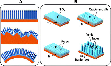 | ||
| Fig. 1 (A) Scheme of nanotube growth on different substrates. Top to bottom: smooth substrate (conducting glass); rough substrate (polycrystalline alumina); flexible substrate (plastic sheet). (B) Schematic diagram of the evolution of a nanotube array by means of potentiostatic mode anodization. | ||
| Ti4+ +2H2O→ TiO2 + 4H+ | (1) |
| TiO2 + 6F− + 4H+→[TiF6]2− + 2H2O | (2) |
Such scheme would be independent from the substrate, and so anodization of titanium layers can be in principle carried out on whatever substrate. Of course, charge transport is mandatory for guaranteeing the process going on, and one can expect that the process ends once the entire layer underwent oxidation.
TiO2 nanotubes on flexible substrate
TiO2 nanotubes on ITO/PET (Fig. 2 (a–b)) prepared in 0.5 wt.% NH4F, 2 mol L−1H2O in glycerol by anodization voltages 25, 35, 50 and 70 V result in very homogeneous size distribution of tubes, with an average inner diameter of approximately 30, 55, 70 and 80 nm, respectively.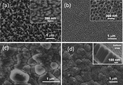 | ||
| Fig. 2 (a–b) SEM top-views of TiO2nanotubular arrays obtained on ITO-PET in 0.5 wt.% NH4F and 2 mol L−1H2O in glycerol at (a) 25 V and (b) 70 V. (c) Rough alumina substrate in which the single grains are visible. (d) SEM images of nanotubular arrays on rough alumina substrates anodized in 0.5 wt.% NH4F, 2 mol L−1H2O in glycerol at 50 V. Conformal grain decoration is visible. Insets in (a), (b) and (d): magnified pictures. | ||
TiO2 nanotubes on alumina substrates
Nanotubular arrays on alumina substrates with different roughness are obtained by anodizing Ti layer in 0.5 wt.% NH4F, 2 mol L−1H2O in glycerol. On flat alumina the average inner diameters of tubes are 45, 55, 65 and 75 nm, respectively, with anodization voltage of 25, 50, 70 and 90 V. In Fig. 2 (c–d)SEM images of morphology of the alumina substrate with high roughness and nanotubes prepared by anodization at 50 V after the deposition of titanium film on this substrate. A uniform distribution of the tubes can be obtained despite of the roughness. Straight tubes have been obtained, which conformal decorate the grains of rough alumina with lateral dimensions ranging between 200 and 1200 nm. This is an interesting and novel result, since it makes available a simple technique for producing aligned TiO2 nanotubes by anodization on highly rough substrates. One typical application, which can benefit of this possibility, is chemoresistive gas sensing, in which availability of nanostructures with high specific surface area is related to possible enhancement of sensitivity.39,40,41,42 Moreover, nanotubes with high surface roughness could be very interesting to increase the surface-related properties such as catalytic activity and gas phase interaction.Anodization of titanium in glycerol-containing electrolyte is a slow process compared to HF-containing electrolyte, but it is still possible to prepare long and well aligned nanotubes. As mentioned before, in HF-based aqueous electrolytes the growth of nanotubes arrays is currently limited up to 500 nm due to the high chemical dissolution rate of TiO2 layer into the solution.33 The possibility to increase the length of nanotubes by varying the anodization parameters such as time, voltage or anodization concentration of NH4F is important.
The morphological characterization of anodized titanium films on ITO/PET, glass/SnO2:F, and alumina substrates shows that highly aligned nanotubes can be achieved over a relatively wide range of anodization voltages (Fig. 3). When the anodization voltage was changed from 25 to 50 V and from 35 to 70 V the average inner diameter of tubes obtained on ITO/PET was increased ∼1.5 times. For nanotubular arrays obtained on alumina substrates when voltage was changed from 50 to 90 V the average inner diameter of tubes increased ∼1.4 times. To obtain nanotubular arrays on ITO-PET and alumina substrates the anodization time was 50–140 min. Tubes were not destroyed and during the long time anodization become longer. During the anodization electrolyte was not heated. In viscous electrolytes fluorine ions mobility is suppressed. Due to suppression of F− ions mobility the walls of tubes were not destroyed. In glycerol based electrolytes chemical dissolution of oxidized titanium is slow process. Therefore well-aligned nanotubes can be prepared and the length of tubes increased by variation of anodization parameters.
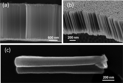 | ||
| Fig. 3 SEM images of the cross-section of TiO2 nanotube arrays formed (a) on PET at 50 V, 140 min, (b) on alumina at 50 V, 60 min, (c) on alumina at 60 V, 90 min (single tube). | ||
Huiming et al.43 prepared TiO2 nanotubular arrays in an electrolyte medium 13 vol% acetic acid and 0.5 vol% HF for 30 min. When the anodization voltage was varied from 5–10 V the average inner diameter of tubes was changed ∼1.5 times. As the voltage was changed 10–20 V, the average inner diameter of tubes was changed ∼2.8 times. But as long as the voltage was increased to 30 V tubes were destroyed. Moreover, ordered tubes morphology was destroyed with long anodization time (1 h).
TiO2 nanotubular structure on titanium sheets
SEM observation of anodized titanium foils at anodization voltage of 80 and 100 V in 0.5% NH4F and 2 mol L−1H2O contained glycerol based electrolyte are shown in Fig. 4a, b. The inner diameter of tubes is 80 and 90 nm, respectively. Well-aligned tubes on titanium sheets with homogeneous distribution were also obtained. In Table 1 the average diameter and length of TiO2 tubes obtained by potentiostatic mode on different substrates are collected.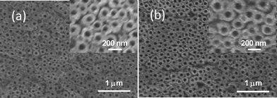 | ||
| Fig. 4 SEM images of anodized titanium sheets in 0.5% NH4F and 2 mol L−1H2O contained glycerol based electrolyte at (a) 80 V and (b) 100 V. | ||
| Substrate | Voltage (V) | Anodization time (min) | Average diameter (nm) | Length (μm) |
|---|---|---|---|---|
| Alumina | 25 | 100 | 45 | 1 |
| 50 | 60 | 55 | 0.9 | |
| 70 | 65 | 1 | ||
| 90 | 50 | 75 | 1 | |
| PET | 25 | 100 | 30 | 0,9 |
| 25 | 140 | 45 | ||
| 35 | 55 | |||
| 50 | 70 | 2,8 | ||
| 50 | 110 | 70 | 2,2 | |
| 70 | 140 | 80 | — | |
| Titanium sheet | 80 | 90 | 80 | — |
| 100 | 90 | — | ||
| Glass/SnO2:F | 50 | 60 | 40 | 0,9 |
The effect of the substrate on nanotube formation in potentiostatic mode can be investigated by considering the pore diameter as a function of the applied voltage (Fig. 5). As can be seen, linear dependence of pore size on the applied voltage is evident at low voltages, while saturation is reached as the voltage increases. Pore size is critically dependent on the substrate providing electron transport: largest pore size corresponds to substrate with highest conductivity. This trend is systematic with respect to three different substrates (i.e.alumina, ITO/PET, Ti foil), indicating the fundamental contribution of the underlying layer to electron conduction. At fixed voltage, more resistive substrate results in lower current, which determines lower etching rate and, as a consequence, reduced pore size. This result indicates that the un-oxidized Ti thin layer contributes to electron transport (and in fact it is the only conducting medium on alumina substrate), but non negligible contribution comes from other sources (like ITO on PET substrates and bulk Ti when Ti foil is considered). Such result indicates the general validity of the model of anodization of Ti layer for tube formation, but indicates significant differences on tube geometry depending on current transport determined by different substrate.
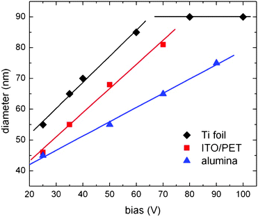 | ||
| Fig. 5 Pore size as a function of the applied voltage on different substrates, namely, alumina, ITO/PET and Ti foil. Straight lines are linear fitting of the experimental data. | ||
TiO2 nanoporous structure on titanium sheets
Surface morphologies by different magnifications of samples anodized in 0.5% NH4F and 2 mol L−1H2O glycerol based electrolyte and in 1 M H2SO4 aqueous solution at constant current are shown in Fig. 6. In aqueous electrolyte containing H2SO4 it is possible to obtain porous structures of TiO2 at very short anodization time. A summary of the anodization conditions by galvanostatic mode is shown in Table 2 and Fig. 7. Porous structures and pore distribution are very homogeneous. Besides the main pores, small pores (∼15–35 nm) are present in all of the samples. When the samples are anodized by current higher than 60 mA·cm−2 small pores with the diameter 20–60 nm appear in big ones. A complete understanding of multimodal size pore formation has not yet been completely gained. However, the process could be rationalized as follows: big pores form in the first stage of anodization, due to the low resistance of metallic titanium. As the anodization proceeds smaller pores are forming, due to enhanced resistance of the oxidized porous layer. Porosity and pore diameter are strongly dependent on current density and anodization time. In H2SO4 containing aqueous electrolyte a variation in pore size up to ∼80 nm was obtained, while in NH4F containing glycerol electrolyte the variation was no more than 30 nm. In the literature, a small pore variation was reported for a 1.4 M H3PO4 electrolyte.44 The anodization process is slow for NH4F contained glycerol electrolyte due to the high dielectric constant and coefficient of viscosity. Hence the dependence of the diffusion constant on the viscosity follows the Stokes–Einstein equation: D = kBT/(6πηrs), where D is the translational diffusion coefficient, kB is Boltzmann′s constant, T is the absolute temperature, η is the dynamic viscosity, and rs is the radius of a spherical body.45,46,47 According to this formula, D is inversely proportional to η. Therefore difference between pore diameters for the samples anodized in NH4F contained glycerol electrolyte was less than in H2SO4 aqueous electrolyte, due to the different viscosity in the two solutions.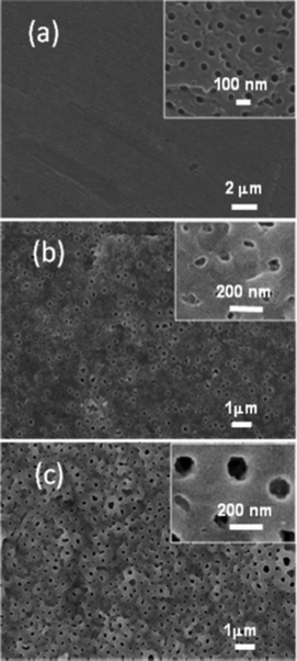 | ||
| Fig. 6 SEM surface morphologies of samples anodized (a) in 0.5% NH4F and 2 mol L−1H2O glycerol based electrolyte at 30 mA, 7 min, (b) in 1M H2SO4 aqueous solution at 10 mA, 30 s, (c) in 1M H2SO4 aqueous solution at 150 mA, 10 s. | ||
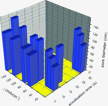 | ||
| Fig. 7 Average pore size as a function of current density and anodization time of Ti sheet anodized by galvanostatic mode. | ||
| Current (mA·cm−2) | Electrolyte | Anodization time (s) | Pore size (nm) |
|---|---|---|---|
| 10 | H2SO4/H2O | 10 | 71 |
| 30 | 85 | ||
| 20 | 15 | 110 | |
| 30 | 110 | ||
| 30 | 10 | 105 | |
| 30 | 123 | ||
| 60 | 5 | 94 | |
| 10 | 121 | ||
| 80 | 5 | 103 | |
| 10 | 122 | ||
| 120 | 5 | 111 | |
| 10 | 131 | ||
| 150 | 5 | 117 | |
| 10 | 147 | ||
| 120 | NH4F/glycerol | 30 | 65 |
| 30 | 420 | 95 |
Functional properties
The nanotubes grown on different substrates have been applied in a series of demonstrator systems to highlight the peculiar functionalities that different substrates bring to nanotubes. In particular, nanotubes on ITO/PET have been applied as photoanodes in a photoelectrochemical cell, nanotubes on alumina substrates have been applied as chemoresistive gas sensors. The functional properties of such demonstrators are collected in Fig. 8 and Fig. 9.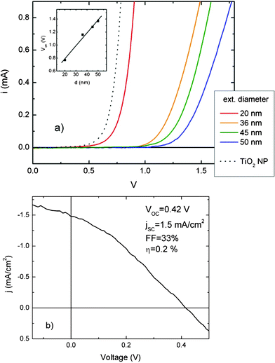 | ||
| Fig. 8 Functional properties of TiO2 nanotubes on different substrates. (a) Current–voltage characteristics of DSCs in dark based on nanotubes with different external diameter on ITO/PET. The functional properties of a DSC based on traditional polycrystalline network (TiO2 nanoparticles 30 nm in diameter) are reported as comparison. (b) Current–voltage characteristics of a DSC under one sun irradiation (AM 1.5 G, 100 mW/cm2), based on nanotubes 20 nm in diameter. | ||
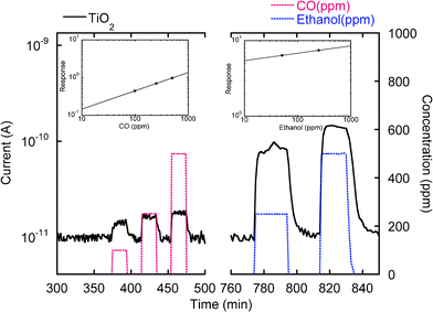 | ||
| Fig. 9 Conductance variation of titania nanotubes as carbon monoxide and ethanol are introduced in the test chamber at a working temperature of 200 °C, 40%RH@20 °C. The left and right insets show the calibration curves for CO and ethanol at the same operation conditions. | ||
The shape of the I–V dark curves in a DSC as a function of pore size, that is the higher ‘on’ bias of nanotube layers compared to nanoparticles and its increase with nanotube external diameter size, can be explained either as an increase of series resistance due to reduction of the area of the TiO2/electrolyte contactor as an increase of the overpotential for reducing the oxidized component of the I3−/I− couple.48 In this latter case the overpotential would be ascribable to an augmenting band bending with structure size at the nanotube/electrolyte interface, in accordance with semiconductor theory of small grains (size of the order of the TiO2 Debye length).49
The functional properties of a DSC based on nanotubes 30 nm in diameter indicate relatively low VOC and jSC, resulting in poor photoconversion efficiency, with respect to up-to-date results on TiO2 nanotube DSCs.15 The main reason is the structural assembly of nanotubes, which are amorphous just after anodization. It has been demonstrated that post growth annealing at T above 350 °C is needed to promote amorphous to anatase transition, resulting in good photovoltaics properties.37,38 However, such procedure requires application of high heat resistant plastic substrate, and its description is out of the scope of the present manuscript.
A representative dynamic response upon exposure with various carbon monoxide and ethanol concentrations is presented in Fig. 9. The conductance increase upon gas exposure is typical for n-type semiconductors interacting with reducing gases. It is worth emphasizing that, irrespective of the preparative conditions, the conductance variations upon injection of the target gas were proportional to the concentration. The interaction with carbon monoxide and ethanol is reversible, an important prerequisite for the sensor technological application. Remarkably, the present system responses, calculated as relative change in conductance, were high (1400% towards 500 ppm of ethanol and 80% towards 500 ppm of carbon oxide), despite the moderate working temperature (200 °C). Calibration curves (Fig. 9 insets) clearly show sensitivity towards CO and ethanol. In addition, the fast responses times (<1 min for a concentration of 500 ppm) were extremely promising features for practical applications. These good performances can be related to the peculiar morphology of titania nanotube arrays, with an average diameter of tubes 45 nm perfectly matching the titania Debye length and making, thus, nanotubes totally depleted under the sensing test conditions. Additional favourable contributions arose from the high surface-to-volume ratio of the present materials arising from their peculiar morphology.
Conclusions
In summary, electrochemical anodization was utilized to obtain nanotubular and nanoporous structures on various un-precedented reported substrates, with the aim of exploiting the peculiar features resulting from the combination of the nanotubes and the substrate for advanced application. In glycerol based electrolytes discrete and well-aligned nanotubes were obtained by potentiostatic mode on a variety of different substrates: flexible PET, smooth and rough alumina, titanium sheet. In case of rough surface tubes are developed as clusters decorating every micro-grain. The length of tubes can be increased more than a few hundred nanometres on different substrates by variation of anodization parameters in glycerol based electrolytes. Galvanostatic mode was applied for production of porous structures using glycerol based and water based electrolytes. The viscosity of electrolyte can discriminate pore size and size distribution. Furthermore, a dynamics of bimodal pore distribution was highlighted, probably due to lower resistance of metallic titanium in the first stages of anodization. Nanotubes grown on different substrates were applied in two demonstrator systems: a DSC and a chemoresistive gas sensor, to highlight the unique functionalities that different substrates bring to nanotubes. It was demonstrated that flexible photoelectrochemical cells can be fabricated using nanotubes on plastic substrates (we refer to last literature achievements for discussion on how enhancing the photoconversion efficiency in such device) and that chemoresistive sensors can be created using nanotubes on alumina. These results pave the way for application of tubular and nanoporous titanium dioxide structures on a variety of end-user applications, with possibility to choose the most suitable technologically enabling substrate. Moreover after demonstrating the feasibility of the preparation technology of titania nanotube on rough alumina substrate, introduction of dopants and catalysts will be investigated to improve chemical sensing performances.References
- T. Gao, G. Meng, Y. Tian, S. Sun, X. Liuand and L. Zhang, J. Phys.: Condens. Matter, 2002, 14, 12651–12656 CrossRef CAS.
- L. Jiang, W. Wang, H. Fuchs and L. Chi, Small, 2009, 5, 2819–2822 CrossRef CAS.
- N. D. Hoa, N. Van Quy, Y. Cho and D. Kim, Sens. Actuators, 2007, B127, 447–454 CAS.
- G. Gorokh, A. Mozalev, D. Solovei, V. Khatko, E. Llobet and X. Correig, Electrochim. Acta, 2006, 52, 1771–1780 CrossRef CAS.
- N. Negishi, T. Iyoda, K. Hashimoto and A. Fujishima, Chem. Lett., 1995, 841–842 CrossRef CAS.
- Y. Gao, M. Nagai, T. C. Chang and J. J. Shyue, Cryst. Growth Des., 2007, 7, 2467–2471 CAS.
- J. J. Wu, G. R. Chen, H. H. Yang, C. H. Ku and J. Y. Lai, Appl. Phys.Lett., 2007, 90213109 Search PubMed.
- P. Zhou, D. Xue, H. Luo and X. Chen, Nano Lett., 2002, 2, 845–847 CrossRef CAS.
- X. Y. Zhang, G. H. Wen, Y. F. Chan, R. K. Zheng, X. X. Zhang and N. Wang, Appl. Phys. Lett., 2003, 83, 3341–3343 CrossRef CAS.
- C. W. Wang, Y. Peng, S. L. Pan, H. L. Zhang and H. L. Li, Acta Physica Sinica, 1999, 482146–2150 Search PubMed.
- S. H. Jeong and K. H Lee, Synth. Met., 2003, 139, 385–390 CrossRef CAS.
- P. L. Chen, J. K. Chang, C. T. Kuo and F. M. Pan, Appl. Phys. Lett., 2005, 861–3 Search PubMed.
- G. K. Mor, K. Shankar, M. Paulose, O. K. Varghese and C. A. Grimes, Nano Lett., 2006, 6, 215–218 CrossRef CAS.
- G. K. Mor, O. K. Varghese, M. Paulose and C. A. Grimes, Advanced Functional Materials, 2005, 151291–1296 Search PubMed.
- O. K. Varghese, M. Paulose and C. A. Grimes, Nat. Nanotechnol., 2009, 4, 592–597 CrossRef CAS.
- Y. Li Xia, L. Sheng Lian, C. Qing Yun and Y. ShouZhuo, Chin. Sci. Bull., 2010, 55, 331–338 CrossRef.
- G. K. M.or, O. K. Varghese, M. Paulose, K. G. Ong and C. A. Grimes, Thin Solid Films, 2006, 49642–48 Search PubMed.
- M. Paulose, O. K. Varghese, G. K. Mor, C. A. Grimes and K.G. Ong, Nanotechnology, 2006, 17398–402 Search PubMed.
- O. K. Varghese, D. Gong, M. Paulose, K. G. Ong, E. C. Dickey and C. A. Grimes, Advanced Materials, 2003, 15624–627 Search PubMed.
- T. Tan, X. XiuFeng, S. Hou De and L. RongFang, Materials Science-Poland, 2008, 26, 487–494 Search PubMed.
- K. C. Popat, L. Leoni, C. A. Grimes and T. A. Desai, Biomaterials, 2008, 28, 3188–3197 CrossRef.
- H. Tsuchiya, J. M. Macak, L. Muller, J. Kunze, F. Muller, P. Greil, S. Virtanen and P. Schmuki, Biomed. Mater. Res., 2006, 77, 534–541 Search PubMed.
- A. Ghicov, H. Tsuchiya, R. Hahn, J. M. Macak, A. G. Munoz and P. Schmuki, Electrochem. Commun., 2006, 8, 528–532 CrossRef CAS.
- G. K. Mor, H. E. Prakasam, O. K. Varghese, K. Shankar and C. A. Grimes, Nano Lett., 2007, 7, 2356–2364 CrossRef CAS.
- M. Paulose, G. K. Mor, O. K. Varghese, K. Shankar and C. A. Grimes, J. Photochem. Photobiol., A, 2006, 178, 8–15 CrossRef CAS.
- Sheng Xu, Shen Yue, Yong Ding and Zhong Lin Wang, Adv. Funct. Mater, 2010, 20, 1–5 Search PubMed.
- A. E. Rakhshani, A. Bumajdad, J. Kokaj and S. Thomas, Appl. Phys, 2009, A97, 759–764 Search PubMed.
- G. K. M.or, O. K. Varghese, M. Paulose, K. Shankar and C. A. Grimes, Sol. Energy Mater. Sol. Cells, 2006, 90, 2011–2075 CrossRef CAS.
- S. Yamabi and H. Imai, Chem. Mater., 2002, 14, 609–614 CrossRef CAS.
- E. Hosono, S. Fujihara, K. Kakiuchi and H. Imai, J. Am. Ceram. Soc., 2004, 126, 7790–7791 CAS.
- V. Zwilling and E. Darque Ceretti, Ann.Chim.Sci. Mater, 1997, 22, 482–493 Search PubMed.
- V. Zwilling, M. Aucouturier and E. Darque-Ceretti, Electrochim. Acta, 1999, 45, 921–929 CrossRef CAS.
- J. M. Macak, H. Tsuchiya, L. Taveira, S. Aldabergerova and P. Schmuki, Angew. Chem., Int. Ed., 2005, 44, 7463–7465 CrossRef CAS.
- Abu Z. Sadek, Haidong Zheng, Kay Latham, Wojtek Wlodarski and Kourosh Kalantar-Zadeh, Langmuir, 2008, 25, 509–514 CrossRef.
- Jan M. Macak, Bin G Gong, Michael Hueppe and Patrik Schmuki, Adv. Mater., 2007, 19, 3027–3031 CrossRef CAS.
- Yuxin Tang, Jie Tao, Yanyan Zhang, Tao Wu, Haijun Tao and Zuguo Bao, Acta Phys.-Chim. Sin., 2008, 24, 2191–2197 CrossRef CAS.
- V. Galstyan, A. Vomiero, I. Concina, A. Braga, M. Brisotto, E. Bontempi, G. Faglia and G. Sberveglieri, Small, 2011, 7, 2437–2442 CrossRef CAS.
- A. Vomiero, V. Galstyan, A. Braga, I. Concina, M. Brisotto, E. Bontempi and G. Sberveglieri, Energy Environ. Sci., 2011, 4, 3408–3413 CAS.
- Alberto Vomiero, Sebastiano Bianchi, Elisabetta Comini, Guido Faglia, Matteo Ferroni and Giorgio Sberveglieri, Cryst. Growth Des., 2007, 7, 2500–2504 CAS.
- G. Sberveglieri, C. Baratto, E. Comini, G. Faglia, M. Ferroni, A. Ponzoni and A. Vomiero, Sens. Actuators, B, 2007, 121, 208 CrossRef.
- Andrea Ponzoni, Camilla Baratto, Sebastiano Bianchi, Elisabetta Comini, Matteo Ferroni, Matteo Pardo, Marco Vezzoli, Alberto Vomiero, Guido Faglia and Giorgio Sberveglieri, IEEESensorsJournal, 2007, 8, 735–742 Search PubMed.
- E. Comini, G. Faglia, M. Ferroni, A. Ponzoni, A. Vomiero and G. Sberveglieri, J. Mol. Catal. A: Chem., 2009, 305, 170–177 CrossRef CAS.
- Huiming Ji, Huixiang Lu, Dongfang Ma, Jianjun Yu and Shicai Ma, Chin. Sci. Bull., 2008, 53, 1352–1357 CrossRef CAS.
- P. Soares, A. Mikowski, C. M. Lepienski, E. Santos, Jr G. A. Soares, V. SwinkaFilho and N. K. Kuromoto, Journal of Biomedical Materials Research Part B: Applied Biomaterials, 2007, 524–530 Search PubMed.
- Jan M. Macak and Patrik Schmuki, Electrochim. Acta, 2006, 52, 1258–1264 CrossRef CAS.
- Bo Chen, E. E. Sigmund and W. P. Halperin, Phys. Rev. Lett., 2006, 96, 145502 CrossRef.
- A. Einstein, Investigation on the Theory of Brownian Motion., 1956 Search PubMed.
- A. J. Bard and R. Faulkner, Electrochemical Methods, Fundamentals and Applications, 2nd edition Wiley, New York ( 2001).Pag.pp. 745–760 Search PubMed.
- (a) J. W. Orton and M. J. Powell, Rep. Prog. Phys., 1980, 43, 1265–1306 CrossRef; (b) J. W. Orton, B. J. Goldsmith, J. A. Chapman and M. J. Powell, J. Appl. Phys., 1982, 53, 1602–1614 CrossRef CAS.
| This journal is © The Royal Society of Chemistry 2011 |