Green-and-red photoluminescence from Si–Si and Ge–Ge bonded network homopolymers and copolymers†
Michiya
Fujiki
*a,
Masahiko
Kato
a,
Yoshiki
Kawamoto
a and
Giseop
Kwak
*b
aGraduate School of Materials Science, Nara Institute of Science and Technology, 8916-5 Takayama, Ikoma, Nara, 630-0036, Japan. E-mail: fujikim@ms.naist.jp; Fax: +81-743-72-6049; Tel: +81-743-72-6040
bDepartment of Polymer Science, Kyungpook National University, 1370 Sankyuk-dong, Buk-gu, Daegu, 702-701, Korea. E-mail: gkwak@knu.ac.kr; Fax: +82-53-950-6623; Tel: +82-53-9507758
First published on 31st January 2011
Abstract
Recently, we found pure green photoluminescence (PL) at 540 nm (2.34 eV) in a vacuum, which is characteristic of a Si–Si bonded network polymer bearing n-butyl groups (organopolysilyne, SNP). SNP was carefully isolated as an orange-yellow solid by avoidance of contact with air and water in the polymer synthesis and PL measurement. This was in contrast with previous reports that SNPs carrying alkyl groups have a blue PL band around 450–480 nm. By applying the modified technique to a soluble Ge–Ge bonded network polymer carrying n-butyl groups (organopolygermyne, GNP), with much care in synthesising the polymer and measuring the PL, we found that GNP reveals a very brilliant red-coloured PL band at 690 nm (1.80 eV) in a vacuum at 77 K. This was in contrast with a previous report that GNP carrying n-hexyl groups has a green PL band at 560 nm (2.21 eV). On the other hand, soluble Si–Ge network copolymers (SGNPs) prepared in a similar way to SNP and GNP syntheses showed green-and-red dual PL bands at 540 nm and 690 nm. Based on analyses with IR, Raman, HR-TEM, XPS, EELS, UV-Vis and PL data, the dual emission was assumed to originate from the coexistence of Si and Ge domains (1–2 nm in diameter), possibly, in the same skeleton of SGNP.
Introduction
Crystalline silicon (c-Si), germanium (c-Ge) and silicon–germanium alloy (SiGe) are the most fundamental inorganic materials for use in microelectronics due to their high carrier mobility and processability. These materials are, however, not suited for Vis-near infrared (Vis-NIR) emitters because of their inherent indirect-type band structures with a relatively narrow optical band gap (Egopt); 1127 nm (1.1 eV) for c-Si and 1880 nm (0.66 eV) for c-Ge, respectively.1 In a previous review paper published in 1986, Brus described that it is possible to tailor the value of Egopt of a cluster by controlling its size in the range of 1.5 nm and sub-μm and that optical phenomena are much different from three-dimensional (3D) bulk materials.2In the late 1980s and in the 1990s, several researchers experimentally demonstrated photoluminescence (PL) phenomenon in the Vis-NIR region from nanocrystal Si (nc-Si) and porous Si (por-Si).3 These reports prompted them to design and produce several low-dimensional Si-based materials theoretically and experimentally.4 The most prominent examples are zero-dimensional (0D) nc-Si as Vis-NIR emitters, one-dimensional (1D) polysilane as a near-UV emitter and a 2D skeleton as a visible emitter, such as a Si–Si bonded network polysilyne and siloxene.
The understanding of low-dimensional Si-based materials encouraged studying a structure–optical property relationship of 0D-, 1D-, 2D-Ge based materials theoretically.5,6 A common approach for Si-based and Ge-based materials is to effectively confine a photoexcited electron-hole pair within the Bohr radius (rB) for Si (rB ≈ 4.9 nm) and for Ge (rB ≈ 24.3 nm).7 However, research on low-dimensional Ge-based materials in the field of chemistry has been delayed.8 The main reason for this situation arises from the limited synthetic approach for soluble Ge–Ge bonded materials using organogermanium sources, which is one thousand times more expensive than the corresponding organosilane sources. However, intense studies focusing on inexpensive Ge-based inorganic sources are, recently, rapidly increasing in the fields of physics and applied physics, which are prepared by molecular beam epitaxy (MBE) technique in an ultrahigh vacuum.9–14
As for solid-state physics, Kanemitsu, Masumoto and coworkers found a broad PL band at 570 nm (2.18 eV) from microcrystalline Ge (μc-Ge) embedded into SiO2 glass at room temperature.9 On the other hand, Stutzmann, Brandt and coworkers reported a near infrared PL band at 920 nm (1.35 eV) for multilayered Ge sheets produced on a solid surface, which is pseudo-2D multilayered Ge crystal called polygermyne, synthesised from CaGe2 as Zintle phase. In contrast, the corresponding pseudo-2D multilayered Si sheets, which are polysilyne terminated with OH polysiloxene and called polysiloxene, prepared by treatment of CaSi2 with HCl aq, showed green PL at 2.39 eV (520 nm).10 However, μc-Ge, polygermyne and polysiloxene are purely inorganic, and hence, are insoluble in any organic solvent.
In 1993, Bianconi et al. first reported the synthesis of a Ge–Ge bonded network organopolygermyne and organopoly(germyne-co-silyne) by reducing n-hexyltrichlorogermane, phenyltrichlorogermane and n-hexyltrichlorosilane with NaK alloy under ultrasound irradiation.15 Organopolygermyne is a soluble model of the insoluble polygermyne. Regardless of this pioneering work, photophysical properties of organopolygermyne have not yet been reported in detail. In 1994, Kishida et al. reported that, at 77 K, poly(n-hexylgermyne) has a green PL band peaking at 560 nm (2.21 eV) whereas poly(n-hexylsilyne) has a blue PL band around 480 nm (2.58 eV).16 The Ge/Si copolymers emitted between these wavelengths, depending on the relative atomic fraction of Ge and Si.16
Recently, we demonstrated that very carefully controlled pyrolysis of various organopolysilynes can create visible PL emitters in the range of 430 to 740 nm, encompassing purple, blue, green, orange, red and deep red colours.17 Alternatively, we observed a pure green PL band at 540 nm (2.34 eV) from a Si–Si bonded network polysilyne with n-butyl groups (SNP) without pyrolysis, which was carefully isolated as an orange-yellow solid by avoidance of contact with air and water during polymer synthesis and PL measurement. This was different from other research groups' reports that poly(n-hexylsilyne) had a blue PL band around 450 nm (2.76 eV) in solution at room temperature18 and 480 nm (2.58 eV) in the solid film at 77 K.16
In this work, by applying our modified technique to a soluble Ge–Ge bonded network organopolygermyne with n-butyl groups (GNP) with careful polymer synthesis and measurement of PL, we demonstrate that GNP reveals a very brilliant red-coloured PL band at 690 nm (1.80 eV) in a vacuum at 77 K without the pyrolysis process. This was in contrast with a previous report of green PL from poly(n-hexylgermyne).16 Furthermore, green-and-red dual emissions of Ge–Ge/Si–Si copolymers (SGNPs), which were prepared by Na-mediated co-condensing organogermanium with organosilane, were observed.
Experimental section
Synthesis of SNP, GNP and SGNPs
GNP and SNP were prepared by Na-mediated condensation of n-butyltrichlorogermane (1, Gelest) and n-butyltrichlorosilane (2, Shin-Etsu), respectively, in hot toluene in the presence of 12-crown-4-ether (2 mol% vs. monomer) under a N2 atmosphere in line with the literature procedure.17 The use of 12-crown-4-ether allowed production of the desired polymer with excellent yield under milder production and safer work-up processes.18SGNPs (x = 0.25, 0.50 and 0.75, x is nominal molar fraction of Si) were produced by Na-mediated co-condensation of 1 and 2 (nominal molar feed ratios: 0.25/0.75, 0.50/0.50 and 0.75/0.25) in a similar manner to the SNP and GNP synthesis. To avoid contact with air and moisture during work-up processes, including preparation, isolation and sample sealing in a glass tube, we typically synthesised GNP in the following manner, as shown in Scheme 1.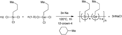 | ||
| Scheme 1 General synthetic scheme of SNP (x = 1.00), GNP (x = 0.00) and SGNPs (x = 0.25, 0.50 and 0.75 in nominal feed fraction). | ||
A 4 mL sample of methylcyclohexane (MCH, TCI, dried over 4A molecular sieves) containing Na (Wako, 0.43 g, 19 mmol) and 12-crown-4-ether (Aldrich, 0.02 g, 0.11 mmol) was placed in a four-necked 100 mL flask, followed by reflux at 120 °C with vigorous stirring at 800 rpm by a mechanical stirring motor with a glass blade. To this mixture, monomer 1 (0.98 g, 5.1 mmol) dissolved in 4 mL MCH was added dropwise with gentle stirring (800 rpm). After the addition was completed, the reaction mixture was gently stirred at 200 rpm for 1 hour, then, allowed to cool to room temperature. The reaction vessel was moved to a glove box filled with 99.9% purity N2 gas.
A clear tan-coloured solution containing GNP, as given in Scheme S1 in the ESI†, was obtained by a pressured filtration of the reaction mixture using a fluorinated membrane filter (Advantec (Tokyo), Labodisc, 0.50 μm pore) to remove the byproduct NaCl and unreacted Na. Fourier-transform infrared (FT-IR) signals due to the νas(Si–O–Si) asymmetric stretching mode around 1000–1100 cm−1 and νs(Si–O–Si) symmetric stretching mode at 800 cm−1 in fresh SNP and SGNP samples were not clearly observed. The weight-average molecular weight (Mw), number-average molecular weight (Mn) and polydispersity index (PDI = Mw/Mn) of isolated GNP are given in Table S1 in the ESI†. The isolated yield of GNP was typically 40–50% when the crude GNP was precipitated into methanol outside the glove box without precaution against air and moisture. This yield was almost identical to a previous report of GNP prepared by NaK alloy under ultrasound irradiation.15 When the work-up process in the glove box was employed, not all yields were determined to have avoided any contact with contaminants during the weighing of samples.
Preparation of GNP films
A MCH solution of SNP, GNP and SGNP was placed into a glass tube (ID 5 mm, OD 7 mm), followed by manually coating the inner wall of the tube and drying by blowing with N2 gas. The film deposited in a glass tube was connected to a two-way vacuum bulb. The tube was moved from the glove box and sealed outside by a vacuum technique (∼0.3 Torr by a rotary pump, ULVAC) with a hand-burner.Characterisation and measurements
The values of Mn and Mw were evaluated by size exclusion chromatography with a UV-Vis photodiode array detector at 40 °C based on a calibration by polystyrene standards on a Shimadzu A10 instrument, and performed using PLgel 10 μm mixed-B (Varian) as a column and tetrahydrofuran (THF) as the eluent. UV-Vis absorption spectra were recorded on a JASCO V-570 spectrophotometer (bandwidth: 1 nm, scanning rate: 100 nm min−1, data sampling: 1 nm interval)). Photo-luminescence (PL) and PL excitation (PLE) spectra in the range of 370 and 1010 nm were measured using a JASCO FP-6600 spectrofluorometer (bandwidth: 5 nm for excitation and 6 nm for emission, response time: 1 s, sensitivity for photomultiplier tube: medium, scanning rate: 1000 nm min−1, data sampling: 1 nm interval) equipped with a housing immersed in liquid N2 designed for phosphorescence measurement (bandwidths: 3 nm for excitation and emission).FT-IR spectra were obtained on a Horiba FT-730 spectrometer (resolution: 4 cm−1, acquisition: 16 times), by casting a solution of the polymers onto a KBr substrate in a N2 atmosphere. Laser Raman spectra were obtained on a JASCO NRS-2100 (Ar CW-laser 514.5 nm, 10 mW) using the back-scattering mode. The polymers sealed in a glass tube and/or placed onto an Au-coated plate in N2 atmosphere were measured.
High-resolution transmission electron microscopy (HR-TEM) images were obtained with a JEOL JEM-3100FEF electron microscope (accelerating voltage: 300 kV, bright image mode). X-Ray photoelectron spectroscopy (XPS) analysis was conducted on a Kratos Axis 165 (Al-Kα, 10 mA, 15 kV). Energy dispersive X-ray spectroscopy (EDS) and electron energy-loss spectroscopy (EELS) were conducted with a JEOL EM-Z01299TJEC. Specimens for HR-TEM/XPS/EELS were prepared by casting an n-hexane solution onto an elastic carbon film-coated microgrid (Oken-Shoji, Tokyo, Japan).
Results and discussion
Characterisation of SNP, GNP and SGNPs by IR, Raman, HR-TEM, XPS and EELS studies
The dimensionality of materials has a pronounced influence on their photophysical properties and electronic structures.4b A prominent example is carbon, where the electronic properties of diamond (sp3), graphene (sp2), nanotubes (sp2) and fullerenes (sp2), that can extend in 3D-, 2D-, 1D- and 0D-materials, differ significantly.10a In a similar way, this concept is applicable to Si, Ge, Sn and Pb though these elements are possible to have 3D-, 2D-, 1D- and 0D-materials based on sp3-hybridisation.4,5,10A question gives rise to tailor an Egopt by the choice of 1D, 2D and 3D structures and by alloying Si and Ge because these elements have isoelectronic structures and an almost identical covalent radii. Note that alloying of a 2D-system has two methods, phase-segregation of a 1D-system corresponding to block-copolymer and a miscible type corresponding to a random copolymer. With the former it is possible to have two Egopt by the two constituents and the latter may exist between Egopt of two constituents. To answer this question, SNP, GNP and SGNPs were characterised by means of IR, Raman, HR-TEM, XPS, EELS, UV-Vis and PL measurements.
Vibrational studies
 | ||
| Fig. 1 IR spectra (a: 4000–400 cm−1 and b: 1500–400 cm−1) of five polymers cast on KBr in pure nitrogen atmosphere. | ||
Marked differences in wavenumber and peak intensities of these six bands due to CH3 and CH2 groups are not evident. However, differences in intensities of the 620 cm−1 band attributable to νas (stretching) of Ge–CH2 in GNP and SGNPs can be seen because the 620 cm−1 band cannot be seen in SNP. Similarly, differences in intensities of the 540 cm−1 and 515 cm−1 bands attributable to νs and νas of Si–Si bond in SNP and SGNPs can be recognised while these bands cannot be seen in the GNP. The 620 cm−1 band is thus characteristic of the Ge-skeleton carrying n-butyl groups. The 540 cm−1 and 515 cm−1 bands are characteristic of a Si-skeleton carrying n-butyl groups.
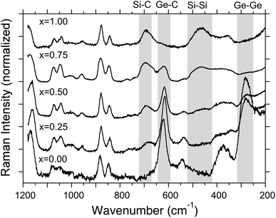 | ||
| Fig. 2 Raman spectra of five polymers cast on Au in pure nitrogen atmosphere. | ||
The four Raman bands (280, 480, 620 and 680 cm−1) combined with the three IR bands (515, 540 and 620 cm−1) become useful fingerprints to characterise bonding states and degree of disorder of the GNP, SNP and SGNPs. However, the Raman band at 880 cm−1 is insensitive to the polymer skeletons and may be used as an internal standard.
If the SGNPs were assumed to be a random copolymer consisting of Si–Si, Ge–Ge and Si–Ge bonds, IR and Raman bands corresponding to the Si–Ge bond may be seen in the range of 300 and 500 cm−1. However, such bands cannot be seen clearly, implying that SGNPs may be not a random copolymer, but rather a block-like (plural-domain-like) skeleton.
HR-TEM, XPS and EELS studies
To characterise atomic fractions of Si and Ge in SGNPs by reference of the SNP and GNP, XPS analysis using a wide scan mode was employed, as shown in Fig. 3. From the analysis given in Table 1, the nominal molar feed fraction of 1 and 2 in SGNPs is not consistent with the atomic fraction of the resulting polymers. A Si moiety is preferentially incorporated into the SGNP, indicating that 2 is approximately two times more reactive than 1 by in the Na-mediated co-condensation reaction with the crown ether.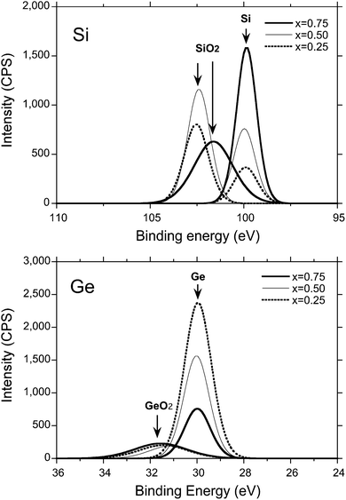 | ||
| Fig. 3 XPS spectra (top: Si 2p peaks; x = 0.25, 0.50, 0.75, bottom: binding energy of Ge 3d peak; x = 0.25, 0.50, 0.75). XPS signals due to SiO2 and GeO2 can be seen due to being partly exposed to air. | ||
| SGNPs (nominal fraction) | Atomic concentration (atomic fraction) | |
|---|---|---|
| Si | Ge | |
| x = 0.75 | 0.79 | 0.21 |
| x = 0.50 | 0.65 | 0.35 |
| x = 0.25 | 0.44 | 0.56 |
To gain a relationship between the Raman band and XPS signal intensities of Ge and Si, the relative 680 cm−1 and 620 cm−1 Raman intensity vs. the 880 cm−1 Raman band was plotted as a function of the atomic Si fraction characterised by XPS analysis, as shown in Fig. 4. An almost linear relationship between the 680 cm−1 Raman intensity and the atomic Si fraction by XPS can be seen while the 620 cm−1 Raman band and atomic Si fraction by XPS may not appear in a linear relationship (Fig. 5).
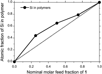 | ||
| Fig. 4 Si fraction characterised by XPS analysis as a function of nominal molar feed fraction of 1 in preparing SGNP. | ||
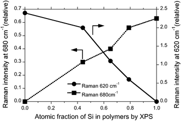 | ||
| Fig. 5 Relative Raman intensities at 680 cm−1 and 620 cm−1 bands vs. the 880 cm−1 band as a function of Si fraction characterised by XPS analysis. | ||
These relative IR/Raman band characteristics along with XPS analytical data may, nevertheless, be useful for characterising Si–Si, Ge–Ge, Si–C, Ge–C and/or Ge–Si bonds and their fractions in homopolymers and copolymers. These IR/Raman spectroscopic and XPS analytical methods, however, cannot definitively exclude the possibility of Si–Ge bonds randomly incorporated into copolymers. To answer the question of why IR/Raman bands due to Si–Ge bonds are clearly not seen, HR-TEM and EELS imaging studies due to heavier Ge may be more straightforward give a possible answer to the above question than the IR/Raman/XPS studies.
HR-TEM images of the SNP, SGNP (x = 0.50) and GNP are shown in Fig. 6. However, it is unclear from these images whether Si and Ge elements are distributed atomically or produce some domains incorporated into the SGNP (x = 0.50) because, in Fig. 6 (right), the dark and white spots with 1–2 nm in diameter can be seen even in pure GNP. To view a distribution of Si and Ge in the SGNP (x = 0.50) by analysing the SNP and GNP in more enhanced high contrast-to-noise ratios, EELS mapping images may show more clearly the existence of Si and Ge domains, as shown in Fig. 7 (bottom, left) and (centre, right), respectively. A distribution of Si and Ge elements appears unclear in HR-TEM images (Fig. 6) and EELS mapping of Si, as shown in Fig. 7 (top, right). From Fig. 7 (top, right), EELS images due to lighter Si elements in SNP and SGNP (x = 0.50) cannot provide conclusive evidence, whether in domains or isolated areas.
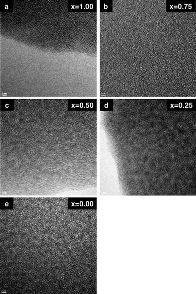 | ||
| Fig. 6 HR-TEM images of (a) SNP (x = 1.00), (b) SGNP (x = 0.75) (c) SGNP (x = 0.50), (d) SGNP (x = 0.25) and (e) GNP (x = 0.00) cast on micro-grid (scale bar (left, bottom) is 2 nm). | ||
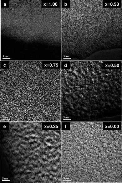 | ||
| Fig. 7 EELS Si mapping of (a) SNP (x = 1.00) and (b) SGNP (x = 0.50). EELS Ge mapping of (c) SGNP (x = 0.75), (d) SGNP (x = 0.50), (e) SGNP (x = 0.25) and (f) GNP (x = 0.00) on micro-grid. Scale bar is 5 nm. | ||
As evident from Fig. 7 (bottom, left), EELS mapping of the heavier Ge element in SGNP (x = 0.25) reveals that Ge elements can be seen as white spots with 1–2 nm in diameter incorporated into SGNP (x = 0.25). The coexistence of white spots due to Ge and dark spots due to Si, which are 1–2 nm in diameter, suggested that Ge and Si elements are segregated into domain-like structures. This situation may be similar to other SGNPs (x = 0.50 and 0.75). These HR-TEM and EELS studies led to the idea that the resulting SGNPs are composed of Ge and Si domains coexisting in the same skeleton, as illustrated in Fig. 8. The segregated structures were assumed to be spontaneously produced in the Na-mediated co-condensation of 1 and 2 due to a difference in chemical reactivity with Na.
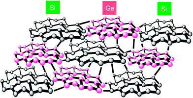 | ||
| Fig. 8 A proposed structure of SGNP with Si- and Ge-domain-like segregation with disordered skeleton. | ||
Photophysical properties
Linear and semi-log UV-Vis absorption of the GNP, SNP and SGNPs (x = 0.25, 0.50, 0.75) in n-hexane as a function of wavelength are given in Fig. 9(a) and (b), respectively. Some differences in these spectra, though subtle, between the polymers can be seen and are weakly dependent on the Si/Ge fraction in the GNP, SNP and SGNPs. The structure-less, broad absorption bands in the range of 200 to 400 nm are due to Mσ–Mσ* (M = Si and Ge) transition and characteristics of the Si–Si and Ge–Ge network skeleton reported previously.15–18 The absorption edge of the GNP, SNP and SGNPs commonly appears at ∼400 nm and the wavelength is weakly dependent on the skeleton elements of the GNP, SNP and SGNPs, as reported previously.16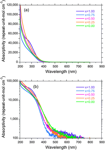 | ||
| Fig. 9 (a) Linear and (b) semi-logarithm UV-Vis absorption spectra of SNP, GNP and SGNPs in n-hexane, 25 °C as a function of wavelength. | ||
The absorption tail around 500–700 nm of GNP and SGNPs could be an evidence of indirect band transition of semiconductors. Another possibility is the Urbach tail that is a measure of degree of disordering. Previously, Kishida et al. characterized this tails using the Urbach tail equation from the viewpoint of amorphous semiconductors.16 Network polymers prepared by Wurtz condensation of n-BuMCl3 (M = Si, Ge) with sodium may be not in an ideal sheet structure with a six-fold-symmetry due to lack of reaction regularity. However, the tail originates from the disordered M–M networks with indirect Mσ–Mσ* transitions.
The Egopt value of ∼690 nm (1.80 eV) is almost consistent with ∼730 nm (1.70 eV) previously estimated by Hajnal et al. based on the band calculation.5c The Egopt value in this work is located between inorganic multilayer polygermyne (920 nm, 1.35 eV)10 and poly(n-hexylgermyne) (560 nm, 2.21 eV).16 As reported already by us,17 the SNP film exhibits brilliant green PL peaking at ∼540 nm (2.34 eV), as demonstrated in Fig. 11, though two independent groups reported that poly(n-hexylsilyne) emits blue PL located at ∼450 nm (2.58 eV)18 and ∼480 nm (2.76 eV).16 The considerable difference in PL wavelengths in the GNP and SNP is attributed to carefully isolated samples by avoidance of contact with air and water in the polymer synthesis and PL measurement in the present experiment procedure, based on the following reasons.
To our experience and knowledge, GNP and SGNPs as well as SNP were very sensitive to a trace amount of air and water. Note that, for purified filtration of polymer solution, polymer samples have to be isolated by a pressured filtration which is a common technique for polymer synthesis, but not a reduced filtration which is a common technique for organic synthesis. We found a considerable change in colour of the fresh samples from deep tan to light tan colour in a week, even if the sample was purged with pure nitrogen gas and stored in the dark. For this reason, we always isolated fresh GNP, SGNPs and SNP samples by precipitating with water-free methanol and coated in a glass tube. The all operations were carried out in a glove box filled with pure nitrogen gas (>99.99%). Even in IR/Raman measurements, we prepared carefully all samples by casting onto KBr in the glove box to avoid any contact to air and water as possible. Furthermore, we used all fresh samples sealed in a vacuum before PL/PLE/UV-Vis measurements. Another possibility of difference between our and previous results16 may ascribe to n-butyl and n-hexyl side groups. The shorter n-butyl group may efficiently protect toward air and moisture due to well-ordered side chain packing while n-hexyl side group may be not so effective due to disordering of side chain packing.
The origin of broad PLE bands of SGNPs around 380–400 nm may come from absorption edge around 400 nm (Fig. 9(a) and (b)). The PLE bands at 380–400 nm might be responsible for the PL bands around 500–560 nm. Also, the PLE bands at 500–560 nm of SGNPs might be responsible for the PL bands around 600–800 nm.
On the other hand, the change in PL spectra of the SNP, GNP and SGNPs (x = 0.25, 0.50, 0.75) as thin film state in a vacuum excited at 360 nm at 77 K is evidently recorded, as shown in Fig. 10. The GNP film itself is found to emit a brilliant red-coloured peak at ∼690 nm (1.80 eV), as evidenced by the photograph (Fig. 11). However, the intensity of the red-PL band at 77 K drastically decreased by approximately one order of magnitude when the specimen was allowed to warm to room temperature, as shown in Fig. S1 (ESI†).
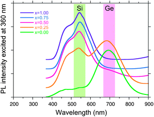 | ||
| Fig. 10 PL spectra (excited at 360 nm) of SNP, GNP and SGNPs thin films in a vacuum at 77 K. | ||
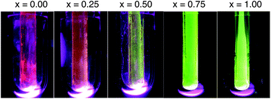 | ||
| Fig. 11 Photographs of network polymers in a vacuum excited at 365 nm with 1.0 mW cm−2 at 77 K. From left to right, GNP (x = 0.00), SGNP (x = 0.25), SGNP (x = 0.50), SGNP (x = 0.75) and SNP (x = 1.00) by nominal molar fraction. | ||
The PL spectra of the SGNPs (x = 0.25 and 0.50) revealed the superposed PL spectra of the corresponding SNP and GNPspectra. The relative PL intensity of SGNP (x = 0.25) at 540 nm and 690 nm is an almost identical. The PL band at 540 nm of SGNP (x = 0.50) is much more intense than that at 690 nm, conversely, only the PL band at 540 nm from the Si-rich SGNP (x = 0.75) is seen. Hence, SGNPs (x = 0.25, 0.50) have green-and-red dual emitting ability, are recognised by photographs (Fig. 11).
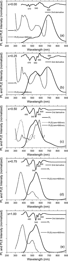
PLE (monitored at several wavelengths), PL (excited at 360 nm) and its second derivative spectra of the SNP, GNP and SGNPs (x = 0.25, 0.50, 0.75) are displayed in Fig. 12. From the PLE spectra of the GNP and SGNP (x = 0.25) monitored at 690 nm, broad PLE bands around 560 nm and 400 nm exist commonly. The former 560 nm PLE band might be responsible for the 680 nm PL band though the existence of the band was unclear from the UV-Vis spectrum (Fig. 9(a) and (b)). The latter 400 nm PLE band is connected to the 680 nm PL band and may be responsible for the absorption tail longer than 350 nm of the peak-less UV-Vis band.
 | ||
| Fig. 12 PLE, PL and second derivative spectra of thin films of SNP, GNP and SGNPs (x = 0.25, 0.50 and 0.75) in a vacuum at 77 K. | ||
From the PLE spectra of the SNP and SGNP (x = 0.75) monitored at 600 nm, broad PLE bands around 500 nm and 380 nm commonly exist. The former 500 nm PLE band might be responsible for the 540 nm PL band though the existence of the band was unclear from UV-Vis spectrum (Fig. 9(a) and (b)). The latter 380 nm PLE band is connected to the 540 nm PL band and may be responsible for an absorption tail longer than 300 nm of the peak-less UV-Vis band. PLE spectra of the SGNP (x = 0.50) monitored at 565 nm and 690 nm indicated the coexistence of plural bands around 580 nm, 480 nm and 360 nm (Fig. 12). By the studies of HR-TEM and EELS analyses of the SGNPs mentioned above, the copolymers are assumed to exist as a collection of the GNP and SNP domains. The coexistence of the GNP and SNP domains is responsible for the green-and-red dual emission property. If the SGNP existed as a random copolymer of Si and Ge, the PL wavelength is assumed to be between 540 nm (2.34 eV) and 690 nm (1.80 eV).
Note that the PL intensity from the GNP is much weaker than that of the SNP by approximately 100–1000 times. This suppression may be related to the large spin-orbit coupling of Ge, leading to the increment of a non-radiative path, such as triplet emission. The PL lifetime measurements of the GNP and SGNPs, hence, were not employed due to this weakness.
A relative large spin-orbit coupling constant (ζ) of Ge (∼6 kcal mol−1), though Si (0.4 kcal mol−1),20 may efficiently suppress the PL intensity of GNP and SGNPs by intersystem crossing and/or non-radiative decay channels. In this regard, as for a relative green-to-red PL intensity of SGNP with x = 0.25 sample, the green PL bands from Si-domains (evaluated to ∼0.45 from Fig. 4) might considerably migrate to the PLE bands at 550–600 nm responsible for the red PL bands by Förster-type energy transfer mechanism, though Ge-domains (evaluated to ∼0.55 from Fig. 4) has an inefficient quantum efficiency. As a result, we observed an almost equal PL intensities of green-and-red PL bands.
The domain size of 1–2 nm of Ge–Ge bonded island-like networks (Fig. 7b) should show the marked quantum confinement effect, proven by the marked blueshift of the corresponding c-Ge which has indirect optical band gap with Eg ≈ 0.66 eV (∼1880 nm).1 However, the domain size, corresponding to the molecular weight of the polymers, was primarily determined by the molecular weights of GNP and SGNPs. Because Bohr radius of c-Ge is ∼24.3 nm, these domain sizes are sufficiently small to confine photoexcited electron-hole pair. Unfortunately, the domain size is limited by Wurtz-condensation reaction of the corresponding n-BuMCl3 (M = Ge, Si) when organic solvent was used.
If we were able to obtain larger domain size upto ∼20 nm, which means ultrahigh molecular weight (Mw) polymer upto 106–107 by an improved polymer synthesis, we will be able to confirm this effect: the optical band gap decreases with an increase of the resulting polymers by the equation of 1/Mw or 1/(Mw)2, approaching a constant value of an ideal infinite 2D-Ge sheet.
Designing and producing direct-gap type semiconductors based on 14-elements are important and challenging issues in recent years. In case of low-dimensional Si family, this goal is almost accomplished by lowering the dimensionality and by tuning the size of semiconducting materials in recent years. GexSi1−x quantum dots by the MBE method showed weak PL peak at 8 K in the range of 0.75 eV (∼1650 nm) and 0.90 eV (∼1350 nm), depending on annealing and substrate temperature.14a
Scanning tunneling spectroscopy study of nc-Ge dots with bilayer thickness deposited on an Si substrate by the MBE elucidated that the band gap increases with decreasing size of the bilayer from ∼1.0 eV (7 nm in size) to 2.5 eV (2 nm in size).14e In a similar way, the band gap of GexSn1−x flatten quantum dots by the MBE increases with decrease of thickness from 0.75 eV (∼1650 nm) to 0.90 eV (∼1350 nm), depending on annealing and substrate temperatures.14h
In our case, GNP which is regarded as a soluble model of nc-Ge monolayer, though the size is limited within 1–2 nm due to polymerization technique, showed clearly a red emission peaking at 690 nm (1.80 eV). This result is predictable by an extension of the nc-Ge bilayer's results.14e The liquid-phase polymerization of 1 with sodium at 120 °C at ambient pressure may provide an alternative approach to obtain visible light emitting Ge-based materials as well as the molecular beam epitaxy deposited onto solid substrate in an ultrahigh vacuum.
The dimensionality of inorganic materials is thus possible to tailor the value of Egopt,10a as shown in Fig. S2 (ESI†). Soluble GNP and SGNP, due to easy coating and dispersion in the form of “Ge-ink” and “SiGe-ink”, may have the benefit of being controlled soluble Si/Ge source materials and may serve as visible emitters covering the green and red regions. A single SGNP source material may offer a new process to produce green-and-red emitters without the SiH4–GeH4CVD process21 in the future. In analogy with SNP,17GNP and SGNP may have other potential in the use of NIR emitters because Si–Ge inorganic alloys with a loss of organic moieties by the pyrolysis process. In recent years, several workers demonstrated preparation and characterisation of Ge nano-clusters capped with organic groups.12b,13,22 Watanabe et al. elucidated that pyrolysis products of soluble Ge nano-clusters capped with organic groups offer semiconducting materials high-carrier mobility and optical waveguide with a high-refractive index value.13 Recently, Klimov et al. reported an NIR PL band at ∼1050 nm (1.18 eV) with a fairly high quantum yield of ∼8% of nc-Ge capped with 1-octadecene, enabling a great reduction of Ge surface oxidation due to formation of strong Si–C bonds.22 The work of pyrolysing GNP and SGNP to achieve NIR PL and semiconducting properties23 is in progress and will be reported as future work.
Conclusions
In this paper, we presented, for the first time, a brilliant red PL band at 690 nm (1.80 eV) from a thin film of GNP at 77 K. The polymer was isolated as a deep tan colour by Na-mediated condensation of 1 in hot toluene with the help of 12-crown-4-ether, followed by avoiding contact with air and water in the polymer synthesis and PL measurement. This was in contrast with the pure green PL band at 540 nm (2.34 eV) of SNP, which was carefully isolated as an orange-yellow solid with special care similar to the synthesis of SNP and the PL measurement, whereas a PL band at 480 nm (2.34 eV) for SNP was reported previously. Furthermore, SGNPs, successfully employed by 1 and 2, have green-and-red dual emission at 540 nm and 690 nm. Analyses using IR, Raman, HR-TEM, XPS, EELS, UV-Vis and PL data indicated that the dual emission originates from the coexistence of Si and Ge domains in the same skeleton of SGNP.Acknowledgements
The work was supported by grants from the Nippon Sheet Glass Foundation for Materials Science and Engineering (FY2009) and a Grant-in-Aid for Science Research in a Priority Area (17067012, FY2005-FY2008) from the Ministry of Education, Culture, Sports, Science and Technology, Japan. The authors thank Prof. Kotohiro Nomura, Dr Masanobu Naito, Dr Hisanari Onouchi, Dr Takuma Kawabe, Shin-ichi Hososhima, Yuji Fujimoto and Tomoki Saito for stimulating discussion and contribution to the preliminary work. MF thanks Prof. Zhang Wei for fruitful discussion and for critical review of the entire text in its original form.Notes and references
- For books, see: (a) Light Emission in Silicon: From Physics to Devices, ed. D. J. Lockwood, Academic, New York, 1998 Search PubMed; (b) J. Linnros, F. Priolo and L. T. Canham, Light Emission from Silicon: Progress Towards Si-Based Optoelectronics, Elsevier, Oxford, 1999 Search PubMed; (c) P. Y. Yu and M. Cardona, Fundamentals of Semiconductors–Physics and Materials Properties, Springer, 3rd edn, 2005 Search PubMed.
- L. Brus, J. Phys. Chem., 1986, 90, 2555–2560 CrossRef CAS.
- (a) S. Furukawa and T. Miyasato, Phys. Rev. B: Condens. Matter Mater. Phys., 1988, 38, 5726–5729 CrossRef CAS; (b) H. Takagi, H. Ogawa, A. Yamazaki, A. Ishizaki and T. Nakagiri, Appl. Phys. Lett., 1990, 56, 2379–2381 CrossRef CAS; (c) A. G. Cullis and L. T. Canham, Nature, 1991, 353, 335–338 CrossRef CAS; (d) V. Lehmann and U. Gösele, Appl. Phys. Lett., 1991, 58, 856–858 CrossRef CAS; (e) Y. Kanemitsu, T. Ogawa, K. Shiraishi and K. Takeda, Phys. Rev. B: Condens. Matter, 1993, 48, 4883–4886 CrossRef CAS; (f) W. L. Wilson, P. F. Szajowski and L. E. Brus, Science, 1993, 262, 1242–1244 CAS; (g) M. V. Wolkin, J. Jorne, P. M. Fauchet, G. Allan and C. Delerue, Phys. Rev. Lett., 1999, 82, 197–200 CrossRef CAS.
- For reviews, see: (a) A. G. Cullis, L. T. Canham and P. E. J. Calcott, J. Appl. Phys., 1997, 82, 909–965 CrossRef CAS; (b) L. Brus, J. Phys. Chem., 1994, 98, 3575–3581 CrossRef CAS; (c) K. Takeda and K. Shiraishi, Comments Condens. Matter Phys., 1997, 18, 91–133 Search PubMed.
- (a) K. Takeda and K. Shiraishi, Chem. Phys. Lett., 1992, 195, 121–126 CrossRef CAS; (b) K. Takeda and K. Shiraishi, Phys. Rev. B: Condens. Matter, 1994, 50, 14916–14922 CrossRef CAS; (c) Z. Hajnal, G. Vogg, L. J.-P. Meyer, B. Szûcs, M. S. Brandt and T. Frauenheim, Phys. Rev. B: Condens. Matter, 2001, 64, 033311 CrossRef; (d) L. E. Ramos, H.-Ch. Weissker, J. Furthmüller and F. Bechstedt, Phys. Status Solidi B, 2005, 242, 3053–3063 CrossRef CAS.
- R. Vrijen, E. Yablonovitch, K. Wang, H. Wen, W. Jiang, A. Balandin, V. Roychowdhury, T. Mor and D. DiVincenzo, Phys. Rev. A: At., Mol., Opt. Phys., 2000, 62, 012306 CrossRef.
- G. Gu, M. Burghard, G. T. Kim, G. S. Düsberg, P. W. Chiu, V. Krstic, S. Roth and W. Q. Han, J. Appl. Phys., 2001, 90, 5747–5751 CrossRef CAS.
- (a) R. D. Miller and R. Sooriyakumaran, J. Polym. Sci., Part A: Polym. Chem., 1987, 25, 111–125 CrossRef CAS; (b) M. Mochida and H. Chiba, J. Organomet. Chem., 1994, 473, 45–54 CrossRef CAS; (c) N. Ostapenko, N. Kozlova, S. Suto, M. Nanjo and K. Mochida, Mol. Cryst. Liq. Cryst., 2008, 497, 20–29 CAS; (d) M. G. Voronkov and K. A. Abzaeva, The Chemistry of Organic Germanium, Tin and Lead Compounds, ed. Z. Rappoport, Wiley, New York, 2002, vol. 2, ch 1 Search PubMed; (e) M. L. Amadoruge and C. S. Weinert, Chem. Rev., 2008, 108, 4253–4294 CrossRef CAS; (f) J. Hlina, J. Baumgartner and C. Marschner, Organometallics, 2010, 29, 5289–5295 CrossRef CAS.
- Y. Maeda, N. Tsukamoto, Y. Yazawa, Y. Kanemitsu and Y. Masumoto, Appl. Phys. Lett., 1991, 59, 3168–3170 CrossRef CAS.
- (a) G. Vogg, M. S. Brandt and M. Stutzmann, Adv. Mater., 2000, 12, 1278–1281 CrossRef CAS; (b) M. S. Brandt, G. Vogg and M. Stutzmann, Silicon Chemistry, ed. P. Jutzi and U. Schubert, Wiley-VCH, Weinheim, 2003, ch. 15, pp. 194–213 Search PubMed.
- M. Zacharias and P. M. Fauchet, Appl. Phys. Lett., 1997, 71, 380–382 CrossRef CAS.
- (a) A. K. Dutta, Appl. Phys. Lett., 1996, 68, 1189–1191 CrossRef CAS; (b) C.-S. Yang, S. M. Kauzlarich and Y. C. Wang, Chem. Mater., 1999, 11, 3666–3670 CrossRef CAS.
- (a) A. Watanabe, M. Uno, F. Hojo and T. Miwa, Chem. Lett., 2002, 662–663 CrossRef CAS; (b) A. Watanabe, F. Hojo and T. Miwa, Appl. Organomet. Chem., 2005, 19, 530–537 CrossRef CAS.
- (a) M. W. Dashiell, U. Denker, C. Müller, G. Costantini, C. Manzano, K. Kern and O. G. Schmid, Appl. Phys. Lett., 2002, 80, 1279–1281 CrossRef CAS; (b) A. P. Li, F. Flack, M. G. Lagally, M. F. Chisholm, K. Yoo, Z. Zhang, H. H. Weitering and J. F. Wendelken, Phys. Rev. B: Condens. Matter Mater. Phys., 2004, 69, 245310 CrossRef; (c) T. S. Shamirzaev, M. S. Seksenbaev, K. S. Zhuravlev, A. I. Nikiforov, V. V. Ul'yanov and O. P. Pchelyakov, Phys. Solid State, 2005, 47, 82–85 CrossRef CAS; (d) X. Lu, B. A. Korgel and K. P. Johnston, Chem. Mater., 2005, 17, 6479–6485 CrossRef CAS; (e) Y. Nakamura, K. Watanabe, Y. Fukuzawa and M. Ichikawa, Appl. Phys. Lett., 2005, 87, 133119 CrossRef; (f) A. D. Schricker, S. V. Joshi, T. Hanrath, S. K. Banerjee and B. A. Korgel, J. Phys. Chem. B, 2006, 110, 6816–6823 CrossRef CAS; (g) P. F. Gomes, F. Iikawa, F. Cerdeira, M. Larsson, A. Elfving, G. V. Hansson, W.-X. Ni and P.-O. Holtz, Appl. Phys. Lett., 2007, 91, 051917 CrossRef; (h) Y. Nakamura, A. Masada and M. Ichikawa, Appl. Phys. Lett., 2007, 91, 013109 CrossRef; (i) P. K. Giri, S. Bhattacharyya, S. Kumari, K. Das, S. K. Ray, B. K. Panigrahi and K. G. M. Nair, J. Appl. Phys., 2008, 103, 103534 CrossRef; (j) X. Chen, M. H. Kim, X. Zhang, C. Larson, D. Yu, A. M. Wodtke and M. Moskovits, J. Phys. Chem. C, 2008, 112, 13797–13800 CrossRef CAS; (k) S. Kim, S. W. Hwang, S.-H. Choi, R. G. Elliman, Y.-M. Kim and Y.-J. Kim, J. Appl. Phys., 2009, 105, 106112 CrossRef.
- W. J. Hymanclki, G. T. Viclscher and P. A. Bianconi, Macromolecules, 1993, 26, 869–871 CrossRef CAS.
- H. Kishida, H. Tachibana, M. Matsumoto and Y. Tokura, Appl. Phys. Lett., 1994, 65, 1358–1360 CrossRef CAS.
- M. Fujiki, Y. Kawamoto, M. Kato, Y. Fujimoto, T. Saito, S. Hososhima and G. Kwak, Chem. Mater., 2009, 21, 2459–2466 CrossRef CAS.
- K. Furukawa, M. Fujino and N. Matsumoto, Macromolecules, 1990, 23, 3423–3426 CrossRef CAS.
- G. Socrates, Infrared and Raman Characteristic Group Frequencies: Tables and Charts, Wiley, 3rd edn, 2004 Search PubMed.
- N. J. Turro, Modern Molecular Photochemistry, University Science Books, 1991 Search PubMed.
- J. Xu, Z.-H. He, K. Chen, X. Huang and D. Feng, J. Phys.: Condens. Matter, 1999, 11, 1631–1637 CrossRef CAS.
- D. C. Lee, J. M. Pietryga, I. Robel, D. J. Werder, R. D. Schaller and V. I. Klimov, J. Am. Chem. Soc., 2009, 131, 3436–3437 CrossRef CAS.
- (a) C.-Y. Wen, M. C. Reuter, J. Bruley, J. Tersoff, S. Kodambaka, E. A. Stach and F. M. Ross, Science, 2009, 326, 1247–1250 CrossRef CAS; (b) R. Soref, Silicon, 2010, 2, 1–6 Search PubMed.
Footnote |
| † Electronic supplementary information (ESI) available: Synthetic condition of SNP, GNP and SGNPs, PL spectra of SNP, GNP and SGNP (x = 0.25, 0.50, 0.75) thin films at 77 K and room temperature, and optical band gap as a function of dimensionality of Si and Ge. See DOI: 10.1039/c0py00345j |
| This journal is © The Royal Society of Chemistry 2011 |