Nanoscale electrical probing of heterogeneous ceramics: the case of giant permittivity calcium copper titanate (CaCu3Ti4O12)
Patrick
Fiorenza
a,
Vito
Raineri
a,
Matthew C.
Ferrarelli
b,
Derek C.
Sinclair
b and
Raffaella
Lo Nigro
*a
aIstituto per la Microelettronica e Microsistemi (IMM), Consiglio Nazionale delle Ricerche (CNR), Strada VIII 5, 95121, Catania, Italy. E-mail: raffaella.lonigro@imm.cnr.it; Fax: +39 095 5968312; Tel: +39 095 5968218
bDepartment of Materials Science and Engineering, University of Sheffield, Sir Robert Hadfield Building, Mappin Street, S1 3JD, Sheffield, UK
First published on 14th January 2011
Abstract
Scanning Probe Microscopy with conductive tips has been used to image and study the dielectric properties of giant permittivity CaCu3Ti4O12 ceramics at the nanoscale. Since measurements are generally carried out on sections of a sample, particular attention has been devoted to possible artefacts due to surface imperfections, such as substantial surface roughness and/or contamination that can result in controversial interpretation, particularly at nanometric spatial dimensions. A reliable surface investigation has been carried out after the definition of both the physical and geometrical unbiased criteria to avoid any artefacts due to surface roughness and/or anomalous tip–sample contact variations. The presence of insulating grain boundaries and the measurement of a depletion layer at the grain–grain boundary interfaces unambiguously demonstrate the relevance of the Internal Barrier Layer Capacitor effect, among all the proposed physical mechanisms, to explain the giant dielectric behaviour. Such imaging provided a clear correlation between the macroscopic dielectric properties and the nanometric structure at the interfaces. Moreover, the “general criteria” for reliable nanoelectrical characterization as well as the related measurement resolution have been defined.
Introduction
Dielectrics are often electrically heterogeneous materials and many among them are complex oxides.1 In this context, calcium copper titanate, CaCu3Ti4O12 (CCTO), represents the most recently debated oxide because of the controversial definition of the origin of its giant permittivity (104–105 in the 101–106 Hz range), which remains constant from 100 to 600 K, while it rapidly drops to 100 below 100 K.2–12 In particular, several macroscopic and also some microscopic scale investigations pointed out the possibility to explain the giant permittivity (k) of CCTO ceramics in terms of an Internal Barrier Layer Capacitor (IBLC) effect.4,5 The IBLC model is widely accepted and implies the presence of conducting parts (grains) surrounded by insulating regions (grain boundaries). On the other hand, the giant permittivities for CCTO single crystals and/or thin films, where no grain boundaries are present, have been also explained by alternative mechanism such as non-ohmic contact between surface and electrode (Surface-Barrier-Layer-Capacitor SBLC effect).13–15However, the giant permittivity phenomenon has been mainly studied and investigated on CCTO ceramics and the IBCL model has been initially proposed on the basis of Impedance Spectroscopy results.4,5 Nevertheless, interpretation of the physical properties of CCTO could certainly be improved by an investigation on the nanometre scale. In fact, several techniques based on Scanning Probe Microscopy (SPM) with conductive tips are useful for such investigation because they generally focus on information about the homogeneity of the sample. In this context, Kelvin Probe Force Microscopy studies on CCTO,12 reinforced the possibility to explain the giant k phenomenon by the IBLC model.
On the other hand, a more recent report based on Conductive Atomic Force Microscopy (C-AFM) measurements of CCTO ceramics claims the presence of conducting grain boundaries, thus proposing the presence of a “percolation conducting network at the grain boundaries plus intragrain insulating interfaces”.16 This interpretation has been challenged by other researchers.17,19
In the present paper, the dielectric behaviour of CCTO ceramics has been studied by C-AFM. The discrepancies among several earlier papers16–19 have been discussed in terms of superficial artefacts affecting the SPM techniques, both from geometrical and electrical considerations. Dedicated methodologies on SPM techniques and sample section surface preparation have been improved to ensure robust and reliable investigation methods, especially working on heterogeneous materials such as CCTO.
In particular, we compare our results to earlier SPM investigations and provide insights towards the controversial interpretation of existing literature data,16–19 merging all of the reported conclusions on the physical nature of the grain boundaries and finally providing the ultimate C-AFM resolution and sensitivity for these heterogeneous materials.
Results and discussion
C-AFM analysis of CaCu3Ti4O12 (CCTO) ceramics
The chemical and electrical nature of CCTO grain boundaries represents a much debated issue. The conducting16,18 or insulating nature4,5,17,19 of the CCTO grain boundaries has been the subject of a harsh debate which has included an animated discussion on the reliability and accuracy of the microscopic measurements. In this context, it should be noted that some data reported in previous literature papers16–19 have been collected from samples prepared under different sintering conditions and it is well-known that the dielectric properties can be affected by the fabrication process. Thus, here, we propose an accurate study on CCTO ceramic pellets fabricated in the same conditions used in previous C-AFM works.16,18The CCTO pellets, before and after the superficial polishing, have been characterized by X-Ray Diffraction (XRD), Scanning Electron Microscopy (SEM) and Energy Dispersive X-ray (EDX) analysis. Comparative studies have been performed on CCTO ceramics before and after the superficial treatments needed for the C-AFM investigation. In both cases they are polycrystalline (Fig. 1a) with grains more than 2 µm wide (Fig. 1b and c) and their stoichiometry is almost ideal (1![[thin space (1/6-em)]](https://www.rsc.org/images/entities/char_2009.gif) :2.87:3.98 Ca:Cu:Ti).
:2.87:3.98 Ca:Cu:Ti).
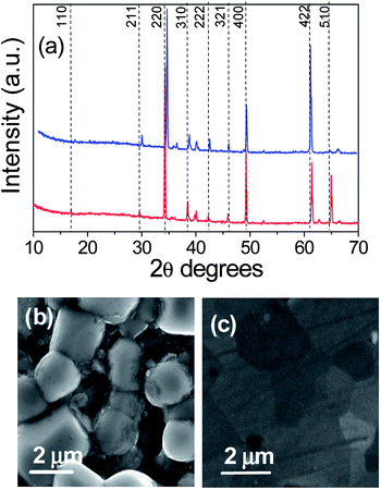 | ||
| Fig. 1 (a) XRD patterns of CCTO ceramics before (red line) and after (blue line) the superficial polishing and SEM images of CCTO ceramics before (b) and after (c) the superficial polishing. | ||
In Fig. 2a the C-AFM current map acquired at 10 V is shown. The darker zones of the current map are associated with more insulating regions, which are located: (i) at the grain boundaries, (ii) some holes among three/four grains and (iii) at the center of few grains. The lower conductivity regions within some grains have been already discussed in an earlier publication20 in terms of CaTiO3 inclusions within single grains. The current value at the grain boundaries is lower than in the grains even if some inclusions are present. The insulating layer thickness (depletion layer) at the grain boundaries is about 100 nm. This value has been evaluated by the full width at half maximum of the peak (see red part in Fig. 2b) visible in the current profile collected along the grain–grain boundary–grain region. This value is in good agreement with our previous Scanning Impedance Microscopy (SIM) investigation.20
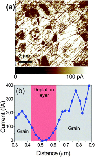 | ||
| Fig. 2 (a) Current map by C-AFM of CCTO ceramics and (b) current profile across the grain–grain boundary–grain structure. | ||
The insulating region is wider than the physical grain boundary thickness (few nanometres) due to the presence of a potential barrier that produces a depletion of the semiconducting (grains) materials.
In the literature, a specific C-AFM study on CCTO showed conducting grain boundaries, even though the SEM images indicated the samples were not well-polished.16 On the other hand, a paper commenting on that C-AFM study claimed that the C-AFM technique is a deficient method to probe ∼nm grain boundaries because of its poor resolution.17
On the basis of these arguments, two main issues now need to be addressed:
- the criteria for reliable nano-electrical characterization, and
- the resolution limit for nano-electrical characterization.
Both issues, in turn, will now be discussed.
SPM reliability
SPM techniques have been developed as important tools for the characterization of surface structures and chemical/physical properties in recent years.21SPM provides the possibility to investigate the electrical, topographic, magnetic and many other types of surface properties down to atomic resolution when physically allowed. Whatever the quality and mode of operation that Scanning Probe Microscopes are based on, the contact area must be kept constant. In the case of SPM applied to the study of electrical properties, the electrical quality of the contact should be validated. In particular, surface roughness and contamination can affect and even destroy the SPM electrical signal, thus the real case can be very far from the ideal one.Flat surfaces favour enhanced lateral resolution even using commercial diamond polycrystalline tips, whose curvature radii are 20–50 nm. This supports the importance of the superficial low roughness requirement. The superficial roughness can be defined in several different ways. Numerous books are available reporting the image processing with matrices, Fourier analysis and statistical methods as autocovariance.21
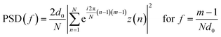
The surface morphology has to be explained in terms of all the superficial components and each AFM image can be considered as the overlap of waves having circular symmetry and can be decomposed by Fast Fourier Transform (FFT). Features with different size and distribution can be present and the Root Mean Square (RMS) of an image height distribution is size (z) dependent. The RMS increases upon increasing the scan size from zero up to the correlation length (Lc), representing the limit for the saturation value to be achieved. This value is defined as the RMS intrinsic value. Moreover, surfaces with different features could possess the same RMS value but different peculiarities. Thus a more independent and confident parameter is the Power Spectral Density (PSD). The PSD(f), where f represents the roughness frequencies, is related to the FFT(f) and RMS by the following equations:
| PSD(f) = |FFT(f)|2 | (1) |
 | (2) |
In fact, an ideal polished surface is described by a Gaussian distribution of the measured surface heights (z(n)) since the typical autocorrelation function for independent events is the Gaussian:
z(n) ∝ exp (−(z − ![[z with combining macron]](https://www.rsc.org/images/entities/i_char_007a_0304.gif) )2/L2c) )2/L2c) | (3) |
 | (4) |
 , f = the frequency range from 1/L to (N/2)/L and L is the digitized profile of length, consisting of N points sampled at intervals of d0 and m is an index related to the component involved in the FFT and it varies from 0 to N. It follows that the PSD(f) of an ideal polished surface should behave as a simple exponential decay vs.f (linear in a semi-logarithmic plot).
In the present work, the complete roughness investigation comes out from the PSD data versus frequency (Fig. 3a) measured on the CCTO surface. Initially, the surface treatment produces a strong roughness reduction eliminating the macroscopic sample defects such as hillocks and surface contamination. The saturation in the region of the lower PSD components (dashed circle in Fig. 3a) is already reached after the treatment with 1 µm diamond paste, indicating that the larger features have been completely removed. The 1 and 0.1 µm diamond paste treatments do not change the lower frequency contribution (already saturated, see the dash circle in Fig. 3a), but there is a strong PSD reduction at higher frequency (full circle). The exponential PSD decay vs.f after the 0.1 µm diamond paste treatment indicates a roughness value comparable to an atomic flat sample in small (about 10 × 10 µm2) scanned regions (RMS ≈ 1 nm in regions which do not include any voids due to ceramic porosity).
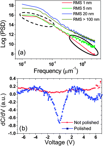 | ||
| Fig. 3 (a) PSD of the topographic CCTO image versus frequency after different superficial treatments and (b) dC/dVversus voltage curves obtained by SCM on both polished (blue curve) and not polished (red curve) CCTO surfaces. | ||
An ideal polished surface, with a very low roughness with respect to the tip radius (10 nm) excludes geometrical artefacts. However, a physical criterion to evaluate the quality of the electrical contact between the sample surface and the nanometre probe needs also to be considered. Here, we suggest monitoring the electrical contact quality (sensitivity) between the probe and the sample surface by checking the Scanning Capacitance Microscopy (SCM) response because this kind of measurement is more sensitive than that obtained directly by C-AFM.
Fig. 3b shows the dC/dVversus voltage curves acquired on both the polished (blue curve) and unpolished (red curve) CCTO surfaces. The electrical sensitivity, as well as the capacitance response, is strongly influenced by surface conditioning. In fact, the dC/dV curve before polishing is almost constant over the whole applied voltage range. This behaviour can be explained with the presence of mobile charges on the sample surface compensating the charge accumulated at the tip/sample interface. In an unpolished condition, a non-quantified amount of charge is present and the contact is degraded. On the other hand, after the polishing treatment the surface shows ideal contact behaviour as in the case of an ideal Metal–Insulator–Semiconductor device or an ideal Schottky contact (blue curve). The peak position is centred on 0 V and this corresponds to a low fixed charge concentration which normally produces the peak shift. The tip therefore “locally probes” the sample properties, i.e. if it is conductive (ohmic response), semi-insulating or insulating (Schottky response) without the influence of surface charges.
As a first conclusion, we can safely confirm that C-AFM investigations on CCTO ceramics are reliable providing the PSD analysis of the surface and the sensitivity evaluation by SCM measurements are performed so as to exclude geometrical and electrical artefacts.
C-AFM spatial resolution
It is well-known that during the commonly used fabrication process for perovskite oxides, a substantial increase in the point defect concentration (including ionic vacancies and free charge carriers) may be produced near the surfaces of each grain, resulting in modification of the dielectric properties. Here we have shown the imaging of such a grain–grain boundary (about 100 nm wide) dielectric structure by accurate C-AFM measurements. However, some authors17 have claimed C-AFM does not have sufficient resolution to investigate grain boundaries.Here, we determine the C-AFM resolution by investigation of an ad hoc fabricated sample. It consists of a 10 nm thermally grown silicon oxide layer on an n-type silicon wafer and on its top a 300 nm thick strongly doped polysilicon layer.
Fig. 4a shows the C-AFM map of the cross-section for the sample which was polished as described previously.
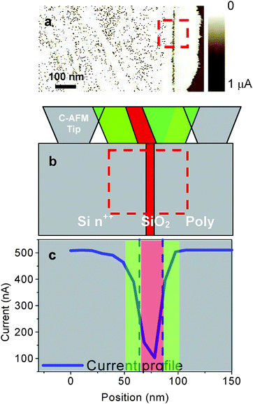 | ||
| Fig. 4 (a) C-AFM on the test sample (Si/SiO2/polySi) cross-section. Three different tip–sample configurations (b) and the current profile (c) across the sample. | ||
The insulating region corresponding to the SiO2 layer is clearly visible as being sandwiched between the two conducting layers. During the C-AFM tip scanning there are three possible configurations identified in Fig. 4b by three different colours: grey, green and red. The grey portions correspond to the tip moving on the conducting polysilicon or silicon substrate. In these regions the current is at the highest level (blue line in grey parts in Fig. 4c). The green portions represent the tip partially overlapping the insulating SiO2 layer (Fig. 4b) and the current value decreases in the profile (blue line in green parts in Fig. 4c). The red portion is related to the tip completely covering the insulating SiO2 layer (Fig. 4b) and the current reaches the minimum value (blue line in red part in Fig. 4c).
The current profile (Fig. 4c) provides an estimation of our C-AFM resolution. In fact, the C-AFM resolution can be obtained by considering the full width at the half maximum of the peak in the current profile: it is 25 nm. The insulating region from the results is larger than the real SiO2 thickness due to the tip size and effective contact area. Thus, with a tip radius 50 nm wide, the diameter of the contact area is 25 nm.
This result demonstrates that the estimated depletion layer at the grain boundaries for the CCTO ceramics is not overestimated because it is larger than the resolution limit, but instead it represents a realistic value.
In this context, it should be noted that the physical thickness of the grain boundaries (generally a few nm) should not be confused with the depletion layer thickness at the grain–grain boundary–grain interfaces. These depletion regions often protrude into the grains and originate from the presence of ionic vacancies, free charge carriers and/or compositional gradients on the outer surfaces of the grains. Their development depends on the defect chemistry of the material under investigation and the processing conditions employed to prepare the samples.
Careful preparation and characterisation of sample surfaces to avoid artefacts and/or errors due to tip–sample interactions ensure that realistic quantification of electrically distinct layers having a thickness of few tens of nanometres can be achieved.
Conclusion
Dielectric investigations on the nanometre scale by C-AFM measurements require a reliable and reproducible characterisation methodology. Here, two criteria have been proposed to carefully control the influence of the superficial features on the roughness (monitoring the PSD data of the surface roughness) and to provide an ideal electric contact between the probe and the sample surface (checking the dC/dV curve behaviour at the nanometre scale by SCM). In CCTO ceramics, semiconducting grains surrounded by insulating regions at the grain boundaries have been observed and because of the evaluation of possible artefacts, the detailed electrical structure at the grain boundaries has been imaged. These results demonstrate the validity of the IBLC effect to explain the macroscopic dielectric properties of CCTO ceramics.Experimental
Fabrication of the CaCu3Ti4O12 ceramics
CaCu3Ti4O12 ceramics have been fabricated by a mixed oxide route already described in previous papers, and have been sintered at 1050 °C.4,5Preparation of CaCu3Ti4O12 ceramics for C-AFM measurements
The ceramic pellets (cut from the original discs) were polished to eliminate the influence of superficial artefacts in the tip contact when mapping by C-AFM. The surface of the CCTO pellets was smoothed by mechanical polishing using diamond pastes, with progressively thinner grid diameters, from 30 to 1 µm. The final polish was performed with a 0.1 µm diamond paste on a frosted glass plate. The final roughness (root mean square) value of the CCTO surface was ∼1 nm (excluding the contribution of voids due to porosity in the ceramics).C-AFM characterization
Power Spectral Density (PSD) analyses have been performed on AFM images acquired in non-contact (tapping) mode with silicon tips (curvature radius ≈ 10 nm).Electrical measurements at the nanometre spatial dimension were carried out by a Digital Instrument D3100 atomic force microscope equipped with a hybrid head and a Nanoscope V controller operating in air and in dark lift mode with diamond tips (curvature radius ≈ 50 nm). The measurements were performed using a back side contact, obtained by silver paint, opposite to the polished surface.
The quality of the electrical contact has been proved using Scanning Capacitance Microscopy (SCM). SCM measurements were carried out in constant ΔV mode. The ac bias applied between the tip and sample was varied in the 1–10 V peak-to-peak range at 90 kHz with the resonator frequency 1.0 ± 0.1 GHz.22
Acknowledgements
This work has been supported by European Union under the project NUOTO (New Materials with Ultrahigh k dielectric constant for Tomorrow wireless electronics). NMP3-CT-2006-032644 and the Engineering and Physical Sciences Research Council (EPSRC).References
- P. Lunkenheimer, S. Krohns, S. Riegg, S. G. Ebbinghaus, A. Reller and A. Loidl, Eur. Phys. J. Spec. Top., 2010, 180, 61 Search PubMed.
- M. A. Subramanian, D. Li, N. Duan, B. A. Reisner and A. W. Sleight, J. Solid State Chem., 2000, 151, 323 CrossRef CAS.
- C. Homes, T. Vogt, S. M. Shapiro, S. Wakimoto and A. P. Ramirez, Science, 2001, 293, 673 CrossRef.
- D. C. Sinclair, T. B. Adams, F. D. Morrison and A. R. West, Appl. Phys. Lett., 2002, 80, 2153 CrossRef CAS.
- T. B. Adams, D. C. Sinclair and A. R. West, Adv. Mater., 2002, 14, 1321 CrossRef CAS.
- W. Li and R. W. Schwartz, Appl. Phys. Lett., 2006, 89, 242906 CrossRef.
- M. H. Cohen, J. B. Neaton, L. He and D. Vanderbilt, J. Appl. Phys., 2003, 94, 3299 CrossRef CAS.
- J. Li, M. A. Subramanian, H. D. Rosenfeld, C. Y. Jones, B. H. Toby and A. W. Sleight, Chem. Mater., 2006, 16, 5223.
- R. Lo Nigro, R. G. Toro, G. Malandrino, M. Bettinelli, A. Speghini and I. L. Fragalà, Adv. Mater., 2004, 16, 891 CrossRef.
- R. Lo Nigro, R. G. Toro, G. Malandrino, I. L. Fragalà, M. Losurdo, M. M. Giangregorio, G. Bruno, V. Raineri and P. Fiorenza, J. Phys. Chem. B, 2006, 110, 17460 CrossRef CAS.
- G. Deng, T. Yamada and P. Muralt, Appl. Phys. Lett., 2007, 91, 202903 CrossRef.
- S.-Y. Chung, I.-D. Kim and S.-J. L. Kang, Nat. Mater., 2004, 3, 774 CrossRef CAS.
- S. Krohns, P. Lunkenheimer, S. G. Ebbinghaus and A. Loidl, Appl. Phys. Lett., 2007, 91, 022910 CrossRef.
- M. Li, Z. Shen, M. Nygren, A. Feteira, D. C. Sinclair and A. West, J. Appl. Phys., 2009, 106, 104106 CrossRef.
- P. Fiorenza, R. Lo Nigro, V. Raineri, G. Malandrino, R. G. Toro and M. R. Catalano, J. Appl. Phys., 2010, 108, 074103 CrossRef.
- D. Fu, H. Taniguchi, T. Taniyama, M. Itoh and S. Koshihara, Chem. Mater., 2008, 20, 1694 CrossRef CAS.
- S. Y. Chung, Chem. Mater., 2008, 20, 6284 CrossRef CAS.
- D. Fu, H. Taniguchi, T. Taniyama, M. Itoh and S. Koshihara, Chem. Mater., 2008, 20, 6286 CrossRef CAS.
- M. C. Ferrarelli, D. C. Sinclair, A. R. West, H. A. Dabkowska, A. Dabkowski and G. M. Luke, J. Mater. Chem., 2009, 19, 5916 RSC.
- P. Fiorenza, R. Lo Nigro, C. Bongiorno, V. Raineri, M. C. Ferarrelli, D. C. Sinclair and A. R. West, Appl. Phys. Lett., 2008, 92, 182907 CrossRef.
- Applied Scanning Probe Methods X, Nanoscience and Technology series, ed. B. Bhushan, H. Fuchs and M. Tomitori, Springer-Verlag, Heidelberg, 2008, ISBN: 978-3-540-74085-8 Search PubMed.
- P. Fiorenza, R. Lo Nigro, V. Raineri, S. Lombardo, R. G. Toro, G. Malandrino and I. L. Fragalà, J. Appl. Phys., 2005, 98, 044312 CrossRef.
| This journal is © The Royal Society of Chemistry 2011 |