Shock-induced breaking in the gold nanowire with the influence of defects and strain rates†
Fenying
Wang
,
Yajun
Gao
,
Tiemin
Zhu
and
Jianwei
Zhao
*
Key Laboratory of Analytical Chemistry for Life Sciences, Ministry of Education, School of Chemistry and Chemical Engineering, Nanjing University, Nanjing, 210008, P. R. China. E-mail: zhaojw@nju.edu.cn; Fax: +86-25-83596523; Tel: +86-25-83596523
First published on 24th February 2011
Abstract
Defects in metallic nanowires have raised concerns about the applied reliability of the nanowires in nanoelectromechanical systems. In this paper, molecular dynamics simulations are used to study the deformation and breaking failure of the [100] single-crystal gold nanowires containing defects at different strain rates. The statistical breaking position distributions of the nanowires show mechanical shocks play a critical role in the deformation of nanowires at different strain rates, and deformation mechanism of the nanowire containing defects is based on a competition between shocks and defects in the deformation process of the nanowire. At low strain rate of 1.0% ps−1, defect ratio of 2% has changed the deformation mechanism because micro-atomic fluctuation is in an equilibrium state. However, owing to strong symmetric shocks, the sensitivity of defects is not obvious before a defect ratio of 25% at high strain rate of 5.0% ps−1.
1. Introduction
In past decade, metallic nanowires have been a focus of research because of their special mechanical,1–3 thermal,4 electrical5,6 and magnetic7 properties. In experiments and applications, constructing defects are known to be of importance for regulating their properties of the metallic nanowires.8–11 In general, the main experimental measures are using scanning tunneling microscopy (STM),12,13atomic force microscopy (AFM),14,15transmission electron microscopy (TEM)16,17 and mechanically controllable break junctions (MCBJ).18,19 However, owing to the small scale of the nanowires, it is a challenge to regulate their defect ratio and manipulate their deformation and breaking failure. Moreover, Hemker20 proposed fundamental description of the nanowire to ensure its reliability must be based on a corresponding understanding of its deformation mechanism when the nanowire is applied as nanoconnector3 and the active component of nanoelectromechanical system (NEMS) devices.21,22 So a good understanding of the properties and behaviors of the metallic nanowires is critical to the success of the design, manufacture, and manipulation of nanodevices.In contrast, Molecular Dynamics (MD) simulations,23,24 which solve Newton's equation of motion for a collection of interacting particles over a number of time steps, are the effective methods to study the deformation and breaking failure of the metallic nanowires. Koh et al.25,26 studied mechanical behaviors of gold and platinum nanowires at different strain rates, indicating that the displayed crystalline-ordered deformation of the nanowire was governed by the formation of a main dislocation plane at low strain rate. Ikeda et al.27 proposed amorphization in nickel nanowires induced by high strain rate. Wang et al.28 studied the structural transformation and breaking mechanism of a single-crystal copper nanowire, and gave paths of deformations at different strain rates. From investigations on the deformation of single-crystal metallic nanowires, we also noticed that defects played an important role in the deformation and breaking failure of the nanowires. For instance, Deng et al.8 discovered that special defects could be utilized to approach a near-ideal strength in gold nanowires through microstructural design. Da Silva et al.29 studied the formation, evolution and breaking of gold nanowires, and they showed how defects led to the formation of one-atom constrictions in the gold nanowires. However, little has been done about the mechanical shock-induced deformation and breaking of the metallic nanowires containing defects, and we do not know which factors will dominate the deformation and the breaking mechanism of the nanowires. In order to make this clear, we focus on MD simulations of the shock-induced tensile deformation and breaking of single-crystal gold nanowires containing defects, which are compared with the corresponding perfect nanowires at low and high strain rates.
It is also worth noting that the nanowires not only have intrinsic properties like bulk materials, but also show special microcosmic behavior owing to nanoscale effects. In our previous work,28,30 the copper nanowire was found to have the most probable breaking position (MPBP) when the nanowire was stretched at different lengths and strain rates. Similar microscopic phenomena in experiments were also found in the metallic and molecular junction conductance following a statistical distribution.31,32 Here, we designed different initial equilibrium states to investigate statistically shock-induced breaking of the [100] single-crystal gold nanowires, which are at different defect ratios and strain rates. As is shown in Fig. 1, we found mechanical shocks played a critical role in the deformation of nanowires at different strain rates. We also proposed a theoretical explanation that a competition between shocks and defects decided the deformation mechanism of the nanowire containing defects.
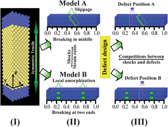 | ||
| Fig. 1 Schematic illustration of the theoretical models The single-crystal gold nanowire is set as 5a × 5a × 15a (a stands for lattice constant, 0.408 nm for gold), corresponding to 1,500 atoms. Strain rates are from 0.1% to 7.0% Ps−1. | ||
2. Methodology
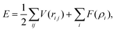
To investigate the influence of defect on the mechanical shock-induced breaking of the gold nanowire under different strain rates, MD simulations were performed to study a total samples of 5100 (17 × 300) of gold nanowires. The geometric models of face centered cubic (FCC) were generated as a regular lattice along the [100] crystallographic orientation. Before stretching gold nanowires applied by uniformly moving the top and bottom fixed layers in the z-direction (Part I in Fig. 1), a different and sufficient relaxation time was firstly adopted to get 300 initial equilibrium states to study statistically the breaking of the nanowire. The strain rates were set from 0.1% to 7.0% ps−1, corresponding to the absolute rates from 0.6 to 428.4 m s−1. With initial equilibrium states, uniaxial tension was applied along the z-direction of the perfect single-crystal gold nanowires at different strain rates. Using statistical analysis, the MPBP is obtained from the fitting peak of breaking position distribution of the perfect single-crystal gold nanowire, and then the position of single layer defects was constructed in the gold nanowire according to the MPBP of the perfect nanowire. In detail, the position of single layer defects was taken as a half of the distance between the MPBP and one fixed layer of the nanowire. As is shown in Fig. 1 (Part II and Part III), the nanowire in Model A was apt to break in the middle part because of slippage at low strain rate, so the single-layer defect was set at defect position A, which was 0.3 in the normalized nanowire. That is, 0.3 is approximately equal to a half of the distance of the MPBP (0.5) and one fixed layer (0.0), considering the ABC arrangement of the FCC structures. Similarly, the nanowire in Model B liked to break at two ends because of local amorphization at high strain rate, so the single layer defect was set at defect position B, which is 0.5 in the normalized nanowire. According to the defect ratio, defect atoms were controlled to be in a uniform distribution on the selected crystal plane. Defect ratios in the nanowires were set from 2% to 25% at low and high strain rates of 1% and 5% ps−1, respectively.In MD simulations, a free boundary condition was adopted. The Verlet leapfrog algorithm was applied for the integration of motion equations to obtain velocity and trajectories of atoms. The Nośe–Hoover thermostat33–35 as a rescaling method of velocity maintained the systems at a constant temperature (300 K). For the simulation methods, tight-binding molecular dynamics (TB-MD)36,37 or Car–Parrinello molecular dynamics (CP-MD)38 simulations can give an accurate result. However, these potential functions have some difficulty in the calculations of the nanowires with large size or many samples. Therefore, the embedded-atom method (EAM) potential developed by Johnson39–41 might be the best choice for this particular purpose. In addition, a statistical analysis and a series of comparisons have been applied in the present study. This methodology may also reduce the systematic error to ensure the reliability of MD simulations. The total energy was given by:
 | (1) |
 | (2) |
 | (3) |
3. Results and discussion
3.1 The deformation characteristics under the effect of defect and strain rate
Fig. 1 shows that mechanical shock decides the breaking position of the nanowire, which is consistent with deformation mechanism. When a defect is constructed, the deformation relays on the competition between defects and shocks, which is related to the type of micro-atomic fluctuation at a certain strain rate. With MD simulations of the [100] single-crystal gold nanowires subjected to the uniaxial tension at strain rates from 0.1% to 7.0% ps−1, Video S1 and S2 (see Supplementary Video S1and S2†) show the representative behaviors of the nanowires at strain rates of 1% and 5% ps−1, respectively. At low strain rate (Video S1), the nanowire remains perfectly crystalline in the deformation process. After the initial elastic deformation, slippage planes appear with only some amorphous structure in the edge of the nanowire. Upon further stretching, the slippage along (111) plane is more and more obvious with increasing strain. Until the overall rupture eventually happens, the nanowire breaks completely along the slippage plane, and symmetric stretching makes slippage in the middle area of the nanowire at low strain rate of 1.0% ps−1. In experiments, the TEM observation50 gave direct evidence that the bulk of the wire remained perfectly crystalline, the sliding took place along the (111) planes, and only the very top of the tip became amorphous. For the slippage, as is known that Burgers vectors exit in the <110> direction along (111) planes when the [100] metallic nanowires subjected to uniaxial tension. It is consistent with slippage mechanism proposed by Finbow et al.51 that the overall dislocation associated with slippage has a Burgers vectors given by (a0/2) [0![[1 with combining macron]](https://www.rsc.org/images/entities/char_0031_0304.gif) 1] in the nanowire. This process could be better described as a uniform slip in the [01] direction of one (111) plane relative to the neighboring one.
1] in the nanowire. This process could be better described as a uniform slip in the [01] direction of one (111) plane relative to the neighboring one.
In contrast, the obvious slippage along (111) plane is not found in the tensile deformation of the nanowire in Video S2. At high strain rate of 5.0% ps−1, the nanowire undergoes a momentum-induced amorphization after the initial elastic deformation, resulting in a glasslike structure over the sample. It is in agreement with previous experimental studies of gold nanowire, such as using MCBJ,48high-resolution transmission electron microscopy (HR-TEM).52 Meanwhile, with increasing strain, the nanowire exhibits superplasticic behavior with amorphous structures during plastic deformation. It is attributed that strong mechanical shocks result in an increase of atomic thermal movements, which facilitates ductility of materials. Upon further stretching, local melted structures appear and the nanowire breaks at two ends under such high strain rate.
Deformation characteristics of the gold nanowires at different strain rates are attributed to micro-atomic fluctuations at the corresponding mechanical shocks. At low strain rate, slippage maintains good crystalline structure during the tensile deformation of the nanowire because weak mechanical shock induces slight micro-atomic fluctuation in an equilibrium state. So the [100] crystallographic orientation shows its particular deformation properties at low strain rate. However, when the high strain rate is applied on the [100] single-crystal gold nanowires, strong mechanical shocks induce acute micro-atomic fluctuation in a non-equilibrium state. Atoms overcome interatomic cohesive energies which brings the breaking of metallic bonds. Thus, due to strong mechanical shock, the effect of strain rate plays a very important role in the deformation of the nanowires at high strain rate.
Considering the influence of defects on the breaking of the nanowires in applications, a single-layer defect is constructed to study the sensitivity of defect to deformation of the [100] single-crystal gold nanowire. In Part III in Fig. 1, defect position A is 0.3 in the normalized nanowire on the base of the middle breaking, which replaces the breaking at low strain rate. Defect position B is at 0.5 in the normalized nanowire according to the breaking at two ends, which is at high strain rate. The defect ratios are set from 2% to 25% in MD simulations. For the [100] gold nanowires at low strain rate of 1% ps−1, Video S3 and S4 show the representative deformation and breaking behaviors of the nanowire with defect ratios of 2% and 10%, respectively (see Supplementary Video S3 and S4†). In comparison with the perfect [100] single-crystal gold nanowire in Video S1, Video S3 shows that slippage appears difficultly for the nanowire with defect ratio of 2%. Under tension, dislocations are firstly observed at the region of constructed defects. As the elongation continues, the dislocations propagate into the bulk of the nanowire and makes local amorphization appear in the symmetric region, which results in the necking around two ends of the nanowire. Then the breaking exhibits at two ends of the nanowire with increasing tensile strain, which was very similar to the structural evolution of perfect single-crystal gold nanowires under a relatively high tensile strain rate. At such a strain rate of 1% ps−1, the deformation mechanism from slippage into local amorphization illustrates there is a competition between defect and shock to the deformation of the nanowire. It is attributable that mechanical trapping induced by atomic defects makes a high local energy area, and a local high energy leads to local melting of crystal structures with the growing of the high energy area, then such equilibrium actions make the nanowire break at two ends at low strain rate of 1% ps−1. Whereas, when defect ratio is 10%, relative good crystal structures are maintained in deformation of the nanowire. With increasing strain, the breaking of the nanowire appears in defect position A (Video S4), which is 0.3 in the normalized nanowire. It is illustrated that the effect of defects with defect ratio of 10% is bigger than mechanical shocks at strain rate of 1% ps−1, and defects decide the breaking position of the nanowire. The existence of the extended structural defects was confirmed by the HR-TEM observation.50
For the influence of defect on deformation behavior of the nanowire at the strain rate of 5% ps−1, Video S5† shows that the nanowire with a defect ratio of 2% exhibits local amorphization with increasing tensile strain, and the nanowire is more likely to break near two ends (Defect position B is 0.5 in the normalized nanowire.). In plastic deformation, the nanowire exhibits superplasticity behavior with increasing tensile strain. When the defect ratio increases to 10%, similar phenomena are found in the stretching processes of the nanowire (Video S6†). Until the defect ratio reaches 25%, the nanowire breaks at the defect position B (Video S7†). In comparison with Video S2 of the perfect nanowire at strain rate of 5.0% ps−1, and Videos S3 and S4 of the nanowires with defect ratio of 2% and 10% at strain rate of 5.0% ps−1, the behaviors in Video S5–S7 show that strain rate effects are of importance to deformation of the nanowires at high strain rate of 5.0% ps−1. This is because strong mechanical shocks induce acute micro-atomic fluctuation of the nanowire. During symmetric tension, shock-induced local amorphous structures play a more important role in the deformation of the nanowire than atomic dislocation at defect position B.
Investigations on the deformation behavior of the nanowires have been achieved a comprehensive understanding about effects of strain rate and defect on micro-atomic fluctuation during the symmetric stretching of the nanowires. The sensitivity of defects to deformation is based on a competition between defects and shocks when the nanowire is subjected to uniaxial tension. According to these properties, the defect position and defect ratio can be controlled to manipulate deformation mechanisms and deformation behaviors of the nanowires, which could give insight into mechanical breaking and operation of metallic nanowires. In addition, the nanowires also could be strengthened near the breaking positions to avoid failure if we could predict their deformation behavior and the final breaking positions of the nanowires.
3.2 The breaking position distributions under effects of defect and strain rate
The final breaking positions of the [100] single-crystal gold nanowires occur at the central part of the nanowires at low strain rates, and the nanowires are apt to break at two ends with increasing strain rate, which could be regulated by defect ratio and defect position. From a microscopic viewpoint, mechanical shock is induced by symmetric stretching at different strain rates, and different mechanical shocks and defect ratios could affect the micro-atomic fluctuation, which could induce different types of shock wave propagation. Holid et al.,53–56 Kadau et al.57 and Bringa et al.58 studied the shock wave propagation in solid materials and gave microscopic mechanism of shock wave propagation was inherently complex in solid materials because the plastic flow was governed by the creation and motion of defects in the deformation of the nanoscale materials.Here, statistical histograms of the final breaking positions are used to illustrate the relationships between macro-breaking position distribution and deformation mechanism induced by micro-atomic fluctuation under effects of strain rate and defect ratio. The statistical histograms of the breaking positions are fitted with Gaussian function, and the fitting peaks replace the most probable breaking position (MPBP) of the nanowires.30Fig. 2(a) shows the breaking position distributions of the [100] prefect single-crystal gold nanowires at strain rates from 0.1% to 7.0% ps−1. The MPBP transfers from the middle area to two ends in the normalized nanowire with increasing strain rate, which is in agreement with the stretching deformation mechanisms under different mechanical shocks. At low strain rates, weak mechanical shocks apply at two ends of the [100] single-crystal gold nanowire, and atomic fluctuation is in an equilibrium state. Slippage along the (111) planes dominates the stretching deformation, and symmetric action induces the overlap of the shock wave in the middle of the nanowire. Energy concentration leads to breaking in the middle area of the nanowire. At high strain rates, the breaking positions distribute at two ends, which is consistent with the deformation mechanism that shock-induced local amorphous decides the breaking points at two ends of the nanowire. With strong mechanical shocks, atomic fluctuation is in a non-equilibrium state during the tensile deformation of the nanowire. Symmetric stretching at high strain rate brings a large stress gradient at two ends, which induces the difficulty of shock wave propagation from two ends to the middle of the nanowire. Thus, shock waves overlap at two ends and the nanowire breaks at two ends.
![The breaking position distributions of the gold nanowires (a) The breaking position distributions of the [100] perfect single-crystal gold nanowires at all the simulated strain rates from 0.1% to 7.0% ps−1; (b) The breaking position distributions of the [100] gold nanowires with defect ratio from 2% to 25% at low strain rate of 1% ps−1; (c) The breaking position distributions of the [100] gold nanowires with defect ratio from 2% to 25% at high strain rate of 5% ps−1. (The dashed lines are the constructed defect positions.)](/image/article/2011/NR/c0nr00797h/c0nr00797h-f2.gif) | ||
| Fig. 2 The breaking position distributions of the gold nanowires (a) The breaking position distributions of the [100] perfect single-crystal gold nanowires at all the simulated strain rates from 0.1% to 7.0% ps−1; (b) The breaking position distributions of the [100] gold nanowires with defect ratio from 2% to 25% at low strain rate of 1% ps−1; (c) The breaking position distributions of the [100] gold nanowires with defect ratio from 2% to 25% at high strain rate of 5% ps−1. (The dashed lines are the constructed defect positions.) | ||
In the statistical histograms of Fig. 2(a), the breaking positions have symmetrical properties for all the strain rates. This is attributed to the deformation mechanism that strong shocks bring local amorphous and weak shocks induce slippage, which correspond to the MPBP at two ends and the MPBP in the middle of the nanowire under high and low strain rates, respectively. However, the counts at high strain rates show asymmetric characteristics at high strain rates. It is because the mechanical shocks are so strong that the breaking of the nanowire shows special microcosmic and uncertain behaviors owing to nanoscale effects. The asymmetric counts should be avoided if there are enough statistical samples. However, there are some difficulties for computers to apply too many samples within the limited time available.
Fig. 2(b) shows the influence of defects on breaking position distributions of the [100] single-crystal gold nanowires at low strain rate of 1% ps−1. Defect ratios range from 2% to 25%. With increasing defect ratio, the MPBP moves from 0.5 (the MPBP of the corresponding perfect nanowire) to 0.3 (the constructed defect position at strain rate of 1% ps−1). When defect ratio is 10%, the MPBP is apt to distribute at defect position A. The breaking position is at 0.3 with increasing defect ratio, indicating that the constructed defect has decided the breaking of the nanowire when defect ratio is larger than 10%. However, it is worth noting that the breaking position distributes at two ends when defect ratio is 2%, which is in agreement with local amorphous at two ends of the nanowires. In comparison with the perfect nanowire at low strain rate of 1% ps−1, the deformation mechanism is transformed from slippage to local amorphous under the influence of defects. This is because defects disrupt micro-atomic fluctuation in the equilibrium state when symmetric stretching is applied at the gold nanowire at low strain rate. A mechanical trap is constructed by atomic defects which induces stress centralization. Due to weak mechanical shocks, slight defects such as defect ratio of 2% can destroy shock wave propagation in the stretching processes of the gold nanowire. The overlapping of shock waves at two ends of the nanowire leads to the changing of deformation mechanism from slippage to local amorphization.
Fig. 2(c) shows the influence of defect on breaking position distributions of the [100] single-crystal gold nanowires at a high strain rate of 5% ps−1. With increasing defect ratio, the MPBP moves from two ends (the MPBP of the perfect nanowire) to 0.5 (the constructed defect position B). In comparison with the breaking position distributions in Fig. 2(b), the breaking distribution of the nanowire at high strain rate of 5% ps−1 is affected notably by defects when the defect ratio is 10%. The breaking distributions of the nanowire is apt to be at the constructed defect position (0.5 in the normalized nanowire) when defect ratio reaches 25%. It is illustrated that the breaking of the nanowire is more sensitive to defects at a low strain rate of 1% ps−1 than at a high strain rate of 5% ps−1. When symmetric stretching is applied at high strain rates, strong symmetric shocks dominate the deformation of the nanowires, and defects do not have sufficient ability to disrupt micro-atomic fluctuation. Large stress gradient induces shock waves overlap at two ends of the nanowire. In shock wave propagation, the concentrated energy induced by a stress gradient is converted to atomic kinetic energy, and metallic bonds break with a direct consequence of atomic kinetic energy overcoming the atomic cohesive energy. Thus, the nanowire tends to break at the two ends and the MPBP are at two ends of the nanowires.
3.3 The mechanical behavior under the effects of defect and strain rate
The deformation and breaking behaviors of the nanowires reflect the influences of defects and mechanical shocks at different strain rates, which can be effectively evaluated by the mechanical properties.1–3,59 Characterization of the mechanical property of metallic materials is using stress–strain relationships, yield stress and Young's modulus, which may provide more insights into the mechanical breaking, material failure and operation of nano-sized devices.
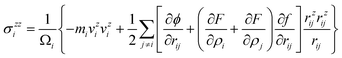
Fig. 3(a) shows the typical stress–strain responses of the [100] single-crystal gold nanowires at strain rates from 0.1% to 7.0% ps−1. The strain (ε) was defined as ε = (l − l0)/l0, where l was the current stretching length and l0 was the length just after relaxation. The strain rate was defined as ![[small epsi, Greek, dot above]](https://www.rsc.org/images/entities/i_char_e0a1.gif) = dε/dt, which was the rate of change in strain with respect to time. The stress (σ) in z-direction was calculated by the Virial scheme.42 As shown in Fig. 3(a), stress increases linearly with increasing strain, which is consistent with elastic law in elastic deformation. (That is σ1 = Yε1, Y is Young's modulus. σ1 and ε1 are strain and stress at the first yield point, respectively, and they are defined as the first yield stress and the first yield strain.) When the stress decreases abruptly, the nanowire undergoes an irreversible deformation indicating the beginning of plastic deformation. Subsequently, the yield cycle repeats continuously with a decreasing trend, and the yield cycle is over when the nanowire has no ability to maintain its structure and finally breaks. The periodicity of the stress–strain fluctuation is more obvious at low strain rate than the one at high strain rate, implying the presence of the temporary stable state in yield cycle at low strain rates.
= dε/dt, which was the rate of change in strain with respect to time. The stress (σ) in z-direction was calculated by the Virial scheme.42 As shown in Fig. 3(a), stress increases linearly with increasing strain, which is consistent with elastic law in elastic deformation. (That is σ1 = Yε1, Y is Young's modulus. σ1 and ε1 are strain and stress at the first yield point, respectively, and they are defined as the first yield stress and the first yield strain.) When the stress decreases abruptly, the nanowire undergoes an irreversible deformation indicating the beginning of plastic deformation. Subsequently, the yield cycle repeats continuously with a decreasing trend, and the yield cycle is over when the nanowire has no ability to maintain its structure and finally breaks. The periodicity of the stress–strain fluctuation is more obvious at low strain rate than the one at high strain rate, implying the presence of the temporary stable state in yield cycle at low strain rates.
![The mechanical behaviors of the gold nanowires. (a) The representative stress–strain relationship of the [100] single-crystal gold nanowire at the strain rates from 0.1% to 7.0% ps−1. (b) The first yield strain, (c) the first yield stress and (d) Young's modulus of the nanowire plotted against strain rates, respectively. (e) The first yield strain, (f) the first yield stress and (g) Young's modulus of the nanowire plotted against defect ratios, respectively. (The defect ratios are from 2% to 25%.)](/image/article/2011/NR/c0nr00797h/c0nr00797h-f3.gif) | ||
| Fig. 3 The mechanical behaviors of the gold nanowires. (a) The representative stress–strain relationship of the [100] single-crystal gold nanowire at the strain rates from 0.1% to 7.0% ps−1. (b) The first yield strain, (c) the first yield stress and (d) Young's modulus of the nanowire plotted against strain rates, respectively. (e) The first yield strain, (f) the first yield stress and (g) Young's modulus of the nanowire plotted against defect ratios, respectively. (The defect ratios are from 2% to 25%.) | ||
Fig. 3(b)–3(d) give the first yield stress, strain and Young's modulus as a function of strain rates, respectively. Strain rates applied to the [100] perfect single-crystal gold nanowires are from 0.1% to 7.0% ps−1, and the average statistical result is from 300 samples for each strain rate. The first yield strain and stress both increase with increasing strain rate. Young's modulus is defined by Sun60 as the stress of a material divided by its strain in the elastic deformation region, which may be used to evaluate the mechanical strength of the nanowires. The average Young's modulus has an increasing trend with increasing strain rate. It is illustrated mechanical shocks from different strain rates are helpful for improving the mechanical strength of metallic materials. For the influence of defect, Fig. 3(e)–3(f) give the first yield stress, strain and Young's modulus as a function of defect ratio at strain rates of 1% and 5% ps−1, respectively. Compared with the mechanical properties of the [100] prefect single-crystal gold nanowire, defects cause an increase of the first yield stress, strain and Young's modulus at strain rates of 1% and 5% ps−1. For example, at the strain rate of 5% ps−1, the increase of the first yield stress (ΔS) is 2.0 GPa from defect ratio of 0% to 2%, and the increase of Young's modulus (ΔY) is 17.5 GPa from defect ratio of 0% to 2%. However, the first yield stress and Young's modulus decrease with increasing defect ratio. The decreasing trends reflect the influence of defects on the breaking of the nanowires. In contrast, the first yield strain of the nanowire is not sensitive to defect ratio within the range of defect ratio. Whether it is at high strain rate or not, the property of the nanowire with low defect ratio indicates the presence of defect-induced hardening effect.
According to these mechanical characteristics in the gold nanowires at low and high strain rates, it is known that mechanical shocks have an influence on mechanical strength, and defects are necessary for improving the mechanical strength within the limitation of defect-induced breaking of the nanowire. The breaking bonds reduce the coordination numbers of defect atoms and increase the strength of the metallic atom bonds. For such considerations, Pauling61 and Goldschmidt62 indicated that the metallic radius of the atom would shrink spontaneously if the coordination number of an atom was reduced. Therefore, coordination number imperfection will shorten the remaining bonds of the under-coordinated atoms and improve the strength of metallic bonds.
4. Conclusion
In summary, we have simulated the [100] single-crystal gold nanowires subjected to symmetric stretching at strain rates from 0.1% to 7.0% ps−1. We have studied the deformation behaviors, mechanical properties and breaking position distributions of the nanowires with defect ratios from 2% to 25% at strain rates of 1.0% and 5.0% ps−1, respectively. We find that: (i) there are two deformation types of the [100] single-crystal gold nanowires under strain rate effects, slippage at low strain rates and local melted structures at two ends of the nanowires induced by high strain rates. There is a competition between defects and shocks in the deformation and breaking of the nanowires. (ii) Macro-breaking position distributions reflect the sensitivity of micro-atomic fluctuation to defects during the symmetric stretching applied to the nanowires. The sensitivity is also affected by mechanical shocks at different strain rates. At a low strain rate of 1.0% ps−1, macro-breaking position distributions exhibit defect-induced breaking when the defect ratio is more than 2%. However, at a high strain rate of 5.0% ps−1, the defect-induced breaking is not obvious until the defect ratio is 25% because of strong symmetric shocks. (iii) For the effects of strain rate and defect on the mechanical properties of [100] single-crystal gold nanowires, mechanical strength increases with increasing strain rate, and defects are helpful for improving the mechanical strength, but mechanical strength decreases slightly with increasing defect ratio.Acknowledgements
This project was supported by the National Natural Science Foundation of China (Grant Nos. 20821063, 20873063 and 51071084), National Basic Research Program of China (973 Program, Grant No. 2007CB936302 and 2010CB732400), the Natural Science Foundation of Jiangsu Province (BK2010389) Specialized Research Fund for the Doctoral Program of Higher Education (SRFDP, 20070284007) and the Open Project of The State Key Laboratory of Physical Chemistry of Solid Surfaces (Xiamen University).References
- J. K. Diao, K. Gall and M. L. Dunn, Nat. Mater., 2003, 2, 656–660 CrossRef CAS.
- M. T. McDowell, A. M. Leach and K. Gaill, Nano Lett., 2008, 8, 3613–3618 CrossRef CAS.
- B. Wu, A. Heidelberg and J. J. Boland, Nat. Mater., 2005, 4, 525–529 CrossRef CAS.
- L. Miao, V. R. Bhethanabotla and B. Joseph, Phys. Rev. A: At., Mol., Opt. Phys., 2005, 72, 134109.
- N. A. Melosh, A. Boukai, F. Diana, B. Gerardot, A. Badolato, P. M. Petroff and J. R. Heath, Science, 2003, 300, 112–115 CrossRef CAS.
- M. A. Reed, C. Zhou, C. J. Muller, T. P. Burgin and J. M. Tour, Science, 1997, 278, 252–254 CrossRef CAS.
- A. S. Alexandrov and V. V. Kabanov, Phys. Rev. Lett., 2005, 95, 076601 CrossRef CAS.
- C. Deng and F. Sansoz, ACS Nano, 2009, 3, 3001–3008 CrossRef CAS.
- O. Gurlu, O. A. O. Adam, H. J. W. Zandvliet and B. Poelsema, Appl. Phys. Lett., 2003, 83, 4610–4612 CrossRef CAS.
- P. L. Gai and M. A. Harmer, Nano Lett., 2002, 2, 771–774 CrossRef CAS.
- J. J. Zhao, C. L. Buia, J. Han and J. P. Lu, Nanotechnology, 2003, 14, 501–504 CrossRef CAS.
- N. Agrait, J. G. Rodrigo, C. Sirvent and S. Vieira, Phys. Rev. B: Condens. Matter, 1993, 48, 8499–8501 CrossRef CAS.
- U. Landman, W. D. Luedtke, B. E. Salisbury and R. L. Whetten, Phys. Rev. Lett., 1996, 77, 1362–1365 CrossRef CAS.
- N. Agrait, G. Rubio and S. Vieira, Phys. Rev. Lett., 1995, 74, 3995–3998 CrossRef.
- P. E. Marszalek, W. J. Greenleaf, H. B. Li, A. F. Oberhauser and J. M. Fernandez, Proc. Natl. Acad. Sci. U. S. A., 2000, 97, 6282–6286 CrossRef CAS.
- S. B. Legoas, D. S. Galvao, V. Rodrigues and D. Ugarte, Phys. Rev. Lett., 2002, 88, 076105 CrossRef.
- V. Rodrigues, T. Fuhrer and D. Ugarte, Phys. Rev. Lett., 2000, 85, 4124–4127 CrossRef CAS.
- C. J. Muller, J. M. Vanruitenbeek and L. J. Dejongh, Phys. Rev. Lett., 1992, 69, 140–143 CrossRef CAS.
- C. J. Muller, J. M. Vanruitenbeek and L. J. Dejongh, Phys. C, 1992, 191, 485–504 CrossRef.
- K. J. Hemker, Science, 2004, 304, 221 CrossRef CAS.
- A. Husain, J. Hone, H. W. C. Postma, X. M. H. Huang, T. Drake, M. Barbic, A. Scherer and M. L. Roukes, Appl. Phys. Lett., 2003, 83, 1240–1242 CrossRef CAS.
- C. M. Lieber, MRS Bull., 2003, 28, 486–491 CAS.
- M. P. Allen and D. J. Tildesley, Computer Simulation of Liquids, Clarendon, New York, 1997 Search PubMed.
- D. C. Rapaport, The Art of Molecular Dynamics Simulation, Cambridge Univerty Press, 2004 Search PubMed.
- S. J. A. Koh and H. P. Lee, Nanotechnology, 2006, 17, 3451–3467 CrossRef CAS.
- A. S. J. Koh and H. P. Lee, Nano Lett., 2006, 6, 2260–2267 CrossRef CAS.
- H. Ikeda, Y. Qi, T. Cagin, K. Samwer, W. L. Johnson and W. A. Goddard, Phys. Rev. Lett., 1999, 82, 2900–2903 CrossRef CAS.
- D. X. Wang, J. W. Zhao, S. Hu, X. Yin, S. Liang, Y. H. Liu and S. Y. Deng, Nano Lett., 2007, 7, 1208–1212 CrossRef CAS.
- E. Z. da Silva, F. D. Novaes, A. J. R. da Silva and A. Fazzio, Phys. Rev. B: Condens. Matter Mater. Phys., 2004, 69, 115411 CrossRef.
- Y. H. Liu, J. W. Zhao and W.F.Y., Phys. Rev. B: Condens. Matter Mater. Phys., 2009, 80, 115417 CrossRef.
- B. Q. Xu and N. J. J. Tao, Science, 2003, 301, 1221–1223 CrossRef CAS.
- P. Reddy, S. Y. Jang, R. A. Segalman and A. Majumdar, Science, 2007, 315, 1568–1571 CrossRef CAS.
- S. Nośe, Mol. Phys., 1984, 52, 255–268 CAS.
- S. Nośe, J. Chem. Phys., 1984, 81, 511–519 CrossRef CAS.
- W. G. Hoover, Phys. Rev. A: At., Mol., Opt. Phys., 1985, 31, 1695–1697 CrossRef.
- M. J. Mehl and D. A. Papaconstantopoulos, Phys. Rev. B: Condens. Matter, 1996, 54, 4519–4530 CrossRef CAS.
- E. Z. da Silva, A. J. R. da Silva and A. Fazzio, Phys. Rev. Lett., 2001, 87, 256102 CrossRef.
- J. Hutter and A. Curioni, ChemPhysChem, 2005, 6, 1788–1793 CrossRef CAS.
- R. A. Johnson, Phys. Rev. B, 1988, 37, 3924–3931 CrossRef.
- R. A. Johnson, Phys. Rev. B, 1988, 37, 6121–6125 CrossRef.
- R. A. Johnson, Phys. Rev. B, 1989, 39, 12554–12559 CrossRef.
- H. A. Wu, Eur. J. Mech. A, 2006, 25, 370–377 CrossRef.
- J. W. Zhao, X. Yin, S. Liang, Y. H. Liu, D. X. Wang, S. Y. Deng and J. Hou, Chem. Res. Chin. Univ., 2008, 24, 367–370 Search PubMed.
- J. Zhao, F. Wang, L. Jiang, X. Yin and Y. Liu, Acta Phys. Chim. Sin., 2009, 25, 1835–1840 Search PubMed.
- Y. H. Liu, F. Y. Wang, J. W. Zhao, L. Y. Jiang, M. Kiguchi and K. Murakoshi, Phys. Chem. Chem. Phys., 2009, 11, 6514–6519 RSC.
- F. Y. Wang, Y. H. Liu, X. Yin, N. Wang, D. X. Wang, Y. J. Gao and J. W. Zhao, J. Appl. Phys., 2010, 108, 074311 CrossRef.
- F. Y. Wang, Y. H. Liu, T. M. Zhu, Y. J. Gao and J. W. Zhao, Nanoscale, 2010, 2, 2818 RSC.
- J. W. Zhao, K. Murakoshi, X. Yin, M. Kiguchi, Y. Guo, N. Wang, S. Liang and H. Liu, J. Phys. Chem. C, 2008, 112, 20088–20094 CrossRef CAS.
- L. Y. Jiang, X. Yin, J. W. Zhao, H. M. Liu, Y. H. Liu, W. F. Y. and J. J. Zhu, J. Phys. Chem. C, 2009, 113, 20193–20197 CrossRef CAS.
- D. R. Strachan, D. E. Johnston, B. S. Guiton, S. S. Datta, P. K. Davies, D. A. Bonnell and A. T. C. Johnson, Phys. Rev. Lett., 2008, 100, 056805 CrossRef.
- G. M. Finbow, R. M. LyndenBell and I. R. McDonald, Mol. Phys., 1997, 92, 705–714 CrossRef CAS.
- V. Rodrigues, F. Sato, D. S. Galvao and D. Ugarte, Phys. Rev. Lett., 2007, 99, 255501 CrossRef CAS.
- B. L. Holian and G. K. Straub, Phys. Rev. Lett., 1979, 43, 1598–1600 CrossRef CAS.
- B. L. Holian, Phys. Rev. A: At., Mol., Opt. Phys., 1988, 37, 2562–2568 CrossRef.
- G. K. Straub, B. L. Holian and R. G. Petschek, Phys. Rev. B, 1979, 19, 4049–4055 CrossRef CAS.
- B. L. Holian, Phys. Rev. A: At., Mol., Opt. Phys., 1988, 37, 2562–2568 CrossRef.
- K. Kadau, T. C. Germann, P. S. Lomdahl and B. L. Holian, Science, 2002, 296, 1681–1684 CrossRef CAS.
- E. M. Bringa, J. U. Cazamias, P. Erhart, J. Stolken, N. Tanushev, B. D. Wirth, R. E. Rudd and M. J. Caturla, J. Appl. Phys., 2004, 96, 3793–3799 CrossRef CAS.
- J. K. Diao, K. Gall and M. L. Dunn, Nano Lett., 2004, 4, 1863–1867 CrossRef CAS.
- C. Q. Sun, Prog. Solid State Chem., 2007, 35, 1–159 CrossRef CAS.
- L. Pauling, J. Am. Chem. Soc., 1947, 69, 542–553 CrossRef CAS.
- V. M. Goldschmidt, Ber. Dtsch. Chem. Ges., 1927, 60, 1263–1296 CrossRef.
Footnote |
| † Electronic supplementary information (ESI) available: Videos S1–S7. See DOI: 10.1039/c0nr00797h |
| This journal is © The Royal Society of Chemistry 2011 |