Electro-netting: Fabrication of two-dimensional nano-nets for highly sensitive trimethylamine sensing†
Xianfeng
Wang
abc,
Bin
Ding
*ab,
Jianyong
Yu
b,
Yang
Si
a,
Shangbin
Yang
c and
Gang
Sun
d
aState Key Laboratory for Modification of Chemical Fibers and Polymer Materials, Donghua University, Shanghai, 201620, China. E-mail: binding@dhu.edu.cn
bNanomaterials Research Center, Modern Textile Institute, Donghua University, Shanghai, 201620, China
cCollege of Textiles, Donghua University, Shanghai, 201620, China
dFibers and Polymer Science, University of California, Davis, CA 95616, USA
First published on 9th December 2010
Abstract
Two-dimensional (2D) polyacrylic acid (PAA) nano-nets that comprise interlinked ultrathin nanowires with diameters of 10–30 nm are successfully prepared by a facile electro-netting process. Nano-nets feature a clear geometric characteristic with ideal and weighted Steiner networks due to the rapid phase separation process and its obeyed minimal energy principle. The versatile nano-nets create enhanced interconnectivity and additional surface area and facilitate the diffusion of analytes into the membranes, which significantly boost the gas diffusion coefficient and sensing properties. As one example, PAA membranes containing fibers and nano-nets used as sensing materials are deposited by electrospinning/electro-netting on an electrode of a quartz crystal microbalance (QCM) for trimethylamine (TMA) detection, which exhibits a quick response (∼180 s), low detection limit (1 ppm) and ideal selectivity at room temperature.
One-dimensional (1D) nanostructures have become the focus of intensive research owing to their fundamental properties and potential applications in nano-scaled devices. Nanofibers represent an important and broad class of 1D nanostructure, standing at the leading edge of nanoscience and nanotechnology. In comparison with other methods of fiber preparation,1electrospinning has emerged as a very attractive approach to the fabrication of micrometre and sub-micrometre fibers under the application of a high voltage to a polymer solution or melt.2,3 The remarkable specific surface area,4 high open porosity,5 and good interconnectivity6 make electrospun nanomaterials highly attractive to different applications ranging from filtration,7 sensors,8drug delivery platforms,9 tissue engineering,10etc..
Recently, growing attempts were reported to regulate the diameter or arrangement of electrospun fibers to achieve the designed functions.11,12 One attractive characteristic of nanofibers correlated with decreased diameter is the increased surface area, which in turn, has immediate repercussions on ultrasensitive sensors and other significant applications. Although diameters as small as 2 to 5 nm have been reported,13 nanofibers smaller than 20 nm in diameter cannot currently be produced uniformly, largely, and repeatedly for most materials systems. Therefore, the major experimental and industrial challenge is to develop robust methods for manufacturing abundant and extremely small nanofibers. Jaeger et al.14 attempted to lower the polymer concentration in the solution to reduce the diameter of electrospun nanofibers, such endeavor simultaneously gave rise to beaded nanofibers. A small quantity of pyridine added to the solution avoided the formation of beaded nanofibers in the course of electrospinning at low concentrations and obtained a handful of ultrathin nanofibers.13 A major breakthrough lies in the direct formation of a large number of net-like structured nanowires with small diameters (∼20 nm) which distribute among conventional electrospun fibers (Fig. 1c). This novel process termed as “electro-netting” allows one-step fabrication of ultrathin “nano-nets” with large quantities and uniform size. Net-like nanowebs, first reported by Ding et al. in 2006, were primitively regarded as a by-product caused by a high electric field that induces instability of suspended charged droplets during electrospinning rather than formed from the breaking jets (Fig. 1a).15 Despite little preceding work on net-like nanowebs, the formation feasibility of nano-nets has been revealed. To date, well-controlled nano-nets in large quantities and a uniform size is still a serious challenge. Furthermore, the exploitation of such novel nano-scaled structures in ultrasensitive sensors and other nanotechnological applications still requires great ingenuity.
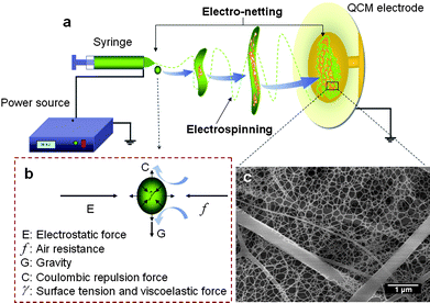 | ||
| Fig. 1 (a) Schematic diagram illustrating the possible formation mechanism of nano-nets during electrospinning/electro-netting deposition of fibrous membranes onto the electrode of QCM. (b) The forces acting on the charged droplet. (c) Typical FE-SEM image of PAA–NaCl (0.1 wt%) nano-nets. | ||
In this communication, we present continuous efforts towards the aim of generating nano-nets with large quantities and uniform size by introducing a certain amount of sodium chloride (NaCl) into the electro-netting polyacrylic acid (PAA) solutions. Nano-nets are expected to have a lasting impact on the quality and scope of the applications. For the first time, the PAA–NaCl composite nano-nets as sensitive coatings were deposited by electro-netting on quartz crystal microbalance (QCM). They were used for trimethylamine (TMA) detection at room temperature, which exhibits improved performance and thus promising applications. Fig. 2 presents the field emission scanning electron microscopy (FE-SEM) images of PAA–NaCl composite nanofibrous membranes (CNMs) with various concentrations of NaCl. As was typical for electrospun fibrous membranes, the resultant nanofibers were randomly oriented as three-dimensional (3D) porous membranes with a wide fiber diameter distribution. These fibrous membranes were reported to have much larger specific surface area than that of flat films.16Fig. 2a shows that the as-prepared PAA fibers have a diameter ranging from 160 to 1600 nm. The joints of the fibers were slightly stuck together due to the incomplete solvent evaporation caused by the formation of the strong hydrogen bond between water and the large amount of carboxyl groups of PAA.17,18 The formation of fiber joints was preferred to prevent the separation between fibers and the electrode of the QCM, making the electrospun fibers useful for practical electronic device applications.19 More interestingly, the formation of a few nano-nets was observed among the PAA fibers. The conventional electrospun PAA fibers acted as a support for the “spider-web-like” nano-nets comprising interlinked 1D nanowires. The corresponding high-magnification FE-SEM image in Fig. 2a confirms that each nanowire has a uniform diameter (∼30 nm), which was one order of magnitude less than that of common electrospun nanofibers. Additionally, the nano-nets exhibit clear geometric characteristics with ideal and weighted Steiner networks,20 in which three neighboring nanowires form a three-way junction with angular symmetry and topological invariability (indicated by the dotted circle). Fig. 1a and 1b present the possible formation mechanism of nano-nets. The instability of the Taylor cone induced by the high electric field results in the formation of the electrospray droplets.21 During the flight of charged droplets from the capillary tip to the collector, the microsized droplet was distorted and expanded into a thin film due to the comprehensive effects of the forces (coulombic repulsion, electrostatic force, air resistance, gravity, surface tension and viscoelastic force) acting on it (Fig. 1b).22,23 The occurrence of rapid phase separation on the splitting-film and its obeyed minimal energy principle may lead to formation of such unexpected structure (Fig. 1a). These versatile nano-nets create enhanced interconnectivity and additional surface area and facilitate the diffusion of analytes into the membranes which may significantly boost the sensing properties.
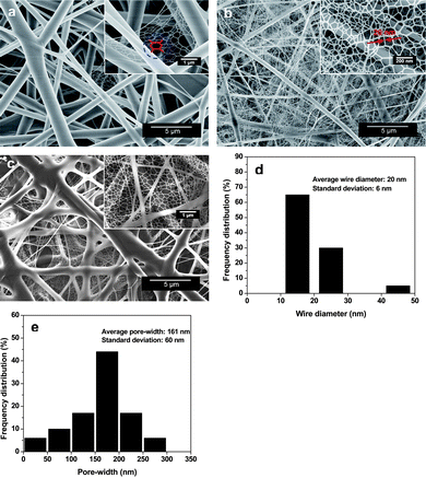 | ||
| Fig. 2 FE-SEM images of PAA–NaCl CNMs formed with a voltage of 30 kV, RH of 25%, and different NaCl concentrations: (a) 0 (pure PAA), (b) 0.1, and (c) 0.2 wt%. (d) Histograms showing the wire diameter distribution and (e) pore-width distribution of the nano-nets shown in (b). | ||
In order to manufacture extremely small nanofibers in large quantities and a uniform size, we considered the addition of salt into the electro-netting PAA solutions, and the results conformed to expectations. Fig. 2b provides the morphology of PAA–NaCl CNMs containing 0.1 wt% NaCl. The fibers showed a dramatically decreased average diameter (526 nm) which corresponded to the sharply increased conductivity.24 A high-magnification FE-SEM image in Fig. 2b clearly shows that dense nano-nets, stacked layer-by-layer, almost completely covering the electrospun fibers and a strong bonding among them was also formed. This result particularly highlights that nano-nets as a main-product have been realized in this study, which further supports the electo-netting process. The larger area density of the nano-nets maybe result from the greatly improved formation probability of microsized droplets due to the increased instability of the Taylor cone after NaCl was added into the polymer solutions. Moreover, deep sighting in the image concluded that nano-nets broke at several points with increased doping of the polymer. This may be due to excessive elongation forces with the concomitant tremendous increase in the solution conductivity (Table 1). As shown in Fig. 2d, the major distribution region (over 65%) of PAA–NaCl nanowire diameters was in the range of 10–20 nm with an average diameter of 20 nm. The region of pore-width distribution of PAA–NaCl nano-nets (Fig. 2e) ranged from 10 to 300 nm, which was much less than that of the pores among electrospun nanofibers. Compared with the conventional nanofibers with large average pore-width (740 nm) used in filtration systems,25 nano-nets posses great potential for application as filters for the removal of particles or viruses with a size in the nanometre range. Further increase in the NaCl concentration (from 0.1 to 0.2 wt %) resulted in a fiber-sticking morphology as well as an increase in the diameter of the spun fibers (Fig. 2c, Table 1) which is in contrast to the conventional view that a more conductive solution causes a reduction in diameter.26 This surface morphology change could be attributed to the localized charge effects on the surface of the fibers,27 as well as changed chain conformation of PAA (from the extended linear conformation to the coil conformation) with increasing ionic strength of the solution,28 causing the fibers to stick together during the formation process. The results from Brunauer-Emmett-Teller (BET) surface area measurements also support these observations (Table 1). At the applied voltage of 30 kV, the PAA–NaCl (0.1 wt%) CNMs show the largest surface areas (6.57 m2 g−1) due to the smallest average fiber diameter and the existing of dense nano-nets (Fig. 2b). Sticking PAA–NaCl (0.2 wt%) CNMs show the largest fiber diameter, whereas the existing of dense nano-nets also possess them with larger surface area (5.91 m2 g−1) than the pure PAA membranes (3.30 m2 g−1).
| Polymer | Additives | Voltage (kV) | Viscosity (cps) | Conductivity (μS m−1) | Average fiber diameter (nm) | Average nanowire diameter (nm) | BET surface area (m2 g−1) |
|---|---|---|---|---|---|---|---|
| PAA | None | 30 | 336 | 6.4 | 835 | 30 | 3.30 |
| 0.1 wt% NaCl | 30 | 337 | 240 | 526 | 20 | 6.57 | |
| 0.2 wt% NaCl | 30 | 330 | 412 | 850 | 28 | 5.91 | |
| 0.1 wt% NaCl | 40 | 337 | 240 | 406 | 14 | 7.91 | |
| 0.1 wt% NaCl | 50 | 337 | 240 | 344 | 11 | 7.97 |
The FE-SEM images in Fig. 3a and 3b show the variation in morphology as the PAA–NaCl (0.1 wt%) CNMs formed at higher applied voltages of 40 and 50 kV, respectively. Similar to the nanofibrous membranes presented in Fig. 2b, uneven and smooth nanofibers binding with ultrathin nanowires were also obtained. It was seen that increasing voltage decreased the average diameters of nanofibers and nanowires, while enhanced the BET surface area of the membranes (Table 1). Additionally, the high-magnification FE-SEM images in Fig. 3a and 3b clearly show that the pore-width and end breakages of the nano-nets are increased with increasing applied voltage. High voltage is able to generate more charges to the solution or droplet surface located at the tip of the needle as well as larger electrostatic forces, both of which stretch the jets fully for the favorable formation of the thinner fibers and completely split nano-nets.29,30 These results indicate that the applied voltage is the prominent factor to regulate the nanowire diameter and pore-width of the nano-nets. Fig. 3c and 3d display SEM images of PAA–NaCl (0.1 wt%) CNMs formed under higher relative humidity (RH) of 45 and 60%, respectively. At a RH of 45%, the incompletely split microsized defect films with multilayered nano-nets were clearly revealed (Fig. 3c, inset). When the RH was increased to 60%, sticking ribbon-like fibers separated the nano-nets into several small parts (Fig. 3d, inset). This could be due to the high RH which retarded the evaporation of solvents from the jets during their flight in the electrostatic field.15
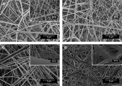 | ||
| Fig. 3 FE-SEM images of PAA–NaCl (0.1 wt%) CNMs obtained at different voltages and RH: (a) 40 kV, 25%; (b) 50 kV, 25%; (c) 30 kV, 45%; (d) 30 kV, 60%. | ||
Nano-nets with large surface area and enhanced interconnectivity are promising for the development of ultrasensitive gas sensors. Fig. 4a depicts the real-time response of membrane coated QCM sensors with three kinds of structures when exposed to increasing TMA concentrations ranging from 1 to 100 ppm. The response undergoes a drastic drop and tends to saturation after several minutes on each injection of TMA in to a chamber. The rapid response time, approximately 180 s to reach 90% of the maximum value for each gas exposure, is comparable to similar TMA exposure levels on polyaniline (PANI)-TiO2 nano-composite coated QCM sensors (∼280 s).31 The pure PAA membrane coated QCM sensors have a slight response (6 Hz) to 1 ppm of TMA. The maximum frequency shifts of the pure PAA membrane coated QCM sensors exposed to 10, 20, 50, and 100 ppm of TMA were 90, 168, 328, and 550 Hz, respectively. It was observed that the sensitivity of sensors to TMA gradually increased with increasing the TMA concentrations. The response caused by the additional mass loading was primarily attributed to the interaction between the TMA molecules and the carboxyl groups of PAA (Fig. 4c, inset).
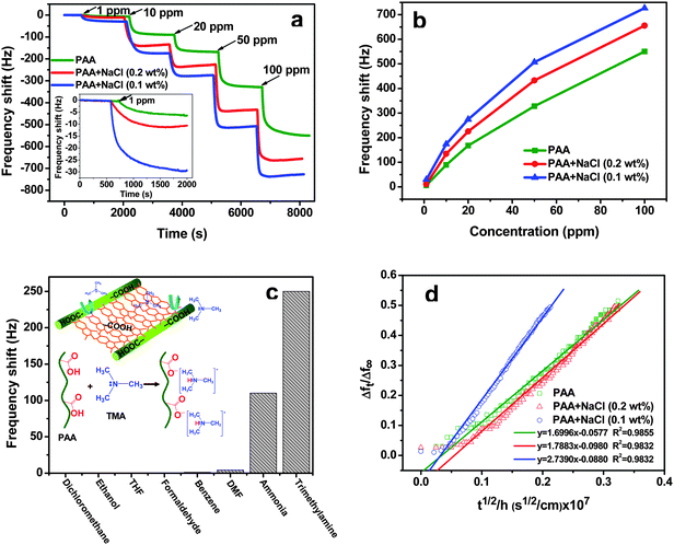 | ||
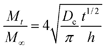
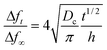
| Fig. 4 (a) Response of sensors coated with PAA–NaCl CNMs containing different concentrations of NaCl (0 (green), 0.1 (blue), and 0.2 wt% (red)) and exposed to increasing TMA concentrations ranging from 1 to 100 ppm. The CNMs were obtained at a voltage of 30 kV and RH of 25%. The coating load was 3500 Hz for each sensor. The inset is the amplified image in the range of 0–2000 s. (b) Frequency shift versusTMA concentration (1–100 ppm) for three nanofibrous membrane coated QCM sensors. (c) Frequency shift of the PAA–NaCl (0.1 wt%) CNMs coated sensor with a coating load of 3500 Hz versus 20 ppm of various VOCs. The inset shows the schematic of gas-sensing mechanism between PAA nano-nets and TMA. (d) Δft/Δf∞ (Δft/Δf∞ < 0.5) as a function of t1/2/h when exposed to 1 ppm of TMA vapours for three nanofibrous membrane coated QCM sensors. The lines are linear fits to Fickian diffusion. | ||
At the low TMA concentration of 1 ppm, the sensors coated with PAA–NaCl CNMs containing 0.1 and 0.2 wt% NaCl exhibited a maximum frequency shift of 30 and 11 Hz, respectively. When exposed to 100 ppm of TMA, the maximum frequency shifts of the sensors coated with PAA, PAA–NaCl (0.1 wt%), and PAA–NaCl (0.2 wt%) CNMs were 550, 727, and 656 Hz, respectively. It can be seen that the gas sensor based on PAA–NaCl (0.1 wt%) CNMs exhibits the best performance, which may be attributable to the abundance of active sites available for faster gas diffusion into the membranes because of the high surface and volume ratio of the nano-nets (Table 1). In comparison with those reported in the literature for QCM sensors coated with PANI film32 and PANI-TiO2 nano-composite,31 which have a detection limit of 5 and 10 ppm for TMA, the PAA–NaCl CNMs covered with dense nano-nets exhibit a reduced detection limit for TMA down to 1 ppm. In addition, the sensing performance of our system is comparable to currently commercially available metal oxide sensors and can be operated at room temperature, unlike the MoO3 sensor that can detect TMA (1 ppm) only at an operating temperature of 300 °C.33
Fig. 4b shows plots of the frequency shifts as a function of TMA concentrations for three kinds of membranes. From the three curves, it is found that the response was proportional to the increasing concentration of TMA from 1 to 20 ppm, but slowly approached saturation when concentrations reached higher levels. Saturation effects like this have been observed previously34 since TMA molecules have to compete for adsorption sites when the TMA concentration becomes high compared with the available absorption sites. This suggests that the sensor may be able to meet practical application demands for the detection of TMA ranging in several concentrations at room temperature.
To identify the effect of the coating load of fibrous membranes on the sensitivity of the sensor, the sensing properties of PAA–NaCl (0.1 wt%) CNMs with a coating load of 1100 Hz were investigated (Fig. S1 in the ESI†). The result clearly demonstrated that QCM sensors with a larger coating load exhibited a larger frequency response for the same TMA concentration because the absorption sites increased as the coating load increased.
With regard to practical use, the selectivity of the QCM sensor is also a concern. For this reason, we performed a sensing test against several conventional volatile organic compounds (VOCs), including ammonia, N,N-dimethylformamide (DMF), tetrahydrofuran (THF), ethanol, benzene, formaldehyde, and dichloromethane, which may act as potential interferences. The test results in Fig. 4c illustrate that the resultant sensors were less sensitive to ammonia, DMF, benzene, and totally insensitive to THF, ethanol, formaldehyde, and dichloromethane. The resultant sensors coated with PAA–NaCl (0.1 wt%) CNMs exhibited an excellent selectivity to TMA.
QCM as an analytical tool is able to detect very tiny mass changes induced by the analyte adsorbed into the polymer films. The change of frequency, Δf, can be converted into a mass change (Δm) according to the Sauerbrey equation:35
| Δf = 2 fo2 Δm/A(μρ)1/2 | (1) |
 | (2) |
 | (3) |
In summary, we have developed an effective way to produce large area density of nano-nets via introducing salt into the electro-netting solutions. Nano-nets that comprise interlinked 1D ultrathin nanowires (∼30 nm) are stacked layer-by-layer and widely distributed in the 3D structure of fibrous membranes. The final morphology of the nano-nets, including nanowire diameter, area density and pore-width of the nano-nets, is highly dependent on the salt concentration, applied voltage and relative humidity. Additionally, PAA–NaCl CNMs as sensitive coatings were deposited by electro-netting on the electrode of QCM for TMA detection at room temperature. The versatile nano-nets created enhanced interconnectivity and additional surface area and facilitated the diffusion of analytes into the membranes, which significantly boosted the gas diffusion coefficient (Dc) and sensing properties. Electro-netted nano-nets are particularly attractive for numerous applications in ultrasensitive sensors as well as ultra-fine filters to intercept viruses and bacteria such as influenza A (H1N1) virus, severe acute respiratory syndrome (SARS) virus, Escherichia coli, etc.
Acknowledgements
This work is supported by the National Natural Science Foundation of China (No. 50803009 and 10872048), the “111 Project” (No. 111-2-04 and B07024), the Shanghai Committee of Science and Technology (No. 10JC1400600), the National Basic Research Program of China (973 Program, 2011CB606100), the Innovation Program of Shanghai Municipal Education Commission and the Fundamental Research Funds for the Central Universities.References
- S. Maheshwari and H. C. Chang, Adv. Mater., 2009, 21, 349–354 CrossRef CAS.
- B. Ding, M. R. Wang, X. F. Wang, J. Y. Yu and G. Sun, Mater. Today, 2010, 13, 16–27 CrossRef CAS.
- Y. Q. Liu, X. P. Zhang, Y. N. Xia and H. Yang, Adv. Mater., 2010, 22, E1–4 CrossRef.
- J. Y. Lin, B. Ding, J. Y. Yu and Y. Hsieh, ACS Appl. Mater. Interfaces, 2010, 2, 521–528 CrossRef CAS.
- Y. Zhu, D. Y. Yang and H. W. Ma, Nanoscale, 2010, 2, 910–912 RSC.
- N. A. M. Barakat, M. A. Kanjwal, F. A. Sheikh and H. Y. Kim, Polymer, 2009, 50, 4389–4396 CrossRef CAS.
- R. Gopal, S. Kaur, Z. W. Ma, C. Chan, S. Ramakrishna and T. Matsuura, J. Membr. Sci., 2006, 281, 581–586 CrossRef CAS.
- X. F. Wang, B. Ding, J. Y. Yu, J. H. He and G. Sun, Int. J. Nonlinear Sci. Numer. Simul., 2010, 11, 509–515 Search PubMed.
- Y. L. Hong, X. S. Chen, X. B. Jing, H. S. Fan, Z. W. Gu and X. D. Zhang, Adv. Funct. Mater., 2010, 20, 1501–1510.
- J. W. Xie, M. R. MacEwan, A. G. Schwartz and Y. N. Xia, Nanoscale, 2010, 2, 35–44 RSC.
- M. Bognitzki, W. Czado, T. Frese, A. Schaper, M. Hellwig, M. Steinhart, A. Greiner and J. H. Wendorff, Adv. Mater., 2001, 13, 70–72 CrossRef CAS.
- H. Q. Cao, H. Zheng, K. Y. Liu and R. P. Fu, Cryst. Growth Des., 2010, 10, 597–601 CrossRef CAS.
- C. B. Huang, S. L. Chen, C. L. Lai, D. H. Reneker, H. Qiu, Y. Ye and H. Q. Hou, Nanotechnology, 2006, 17, 1558–1563 CrossRef.
- R. Jaeger, H. Schonherr and G. J. Vancso, Macromolecules, 1996, 29, 7634–7636 CrossRef CAS.
- B. Ding, C. R. Li, Y. Miyauchi, O. Kuwaki and S. Shiratori, Nanotechnology, 2006, 17, 3685–3691 CrossRef CAS.
- X. F. Wang, B. Ding, J. Y. Yu, M. R. Wang and F. K. Pan, Nanotechnology, 2010, 21, 055502 CrossRef.
- J. Y. Huang, X. Q. Li and Q. P. Guo, Eur. Polym. J., 1997, 33, 659–665 CrossRef CAS.
- J. Du and Y. L. Hsieh, Nanotechnology, 2008, 19, 125707 CrossRef.
- X. F. Wang, B. Ding, M. Sun, J. Y. Yu and G. Sun, Sens. Actuators, B, 2010, 144, 11–17 CrossRef.
- G. S. Li, Y. J. Yin, Y. Li and Z. Zhong, Chin. Sci. Bull., 2009, 54, 3220–3224 CrossRef.
- G. Larsen, R. Spretz and R. Velarde-Ortiz, Adv. Mater., 2004, 16, 166–169 CrossRef CAS.
- X. H. Zong, K. Kim, D. F. Fang, S. F. Ran, B. S. Hsiao and B. Chu, Polymer, 2002, 43, 4403–4412 CrossRef CAS.
- R. L. Grimm and J. L. Beauchamp, J. Phys. Chem. B, 2005, 109, 8244–8250 CrossRef CAS.
- L. W. Ji, A. J. Medford and X. W. Zhang, Polymer, 2009, 50, 605–612 CrossRef CAS.
- X. H. Qin and S. Y. Wang, J. Appl. Polym. Sci., 2006, 102, 1285–1290 CrossRef CAS.
- C. Kim, B. T. N. Ngoc, K. S. Yang, M. Kojima, Y. A. Kim, Y. J. Kim, M. Endo and S. C. Yang, Adv. Mater., 2007, 19, 2341–2346 CrossRef CAS.
- A. C. Patel, S. X. Li, C. Wang, W. J. Zhang and Y. Wei, Chem. Mater., 2007, 19, 1231–1238 CrossRef.
- B. Kim, H. Park, S. H. Lee and W. M. Sigmund, Mater. Lett., 2005, 59, 829–832 CrossRef CAS.
- S. A. Theron, E. Zussman and A. L. Yarin, Polymer, 2004, 45, 2017–2030 CrossRef CAS.
- R. Nirmala, K. T. Nam, S. J. Park, Y. S. Shin, R. Navamathavan and H. Y. Kim, Appl. Surf. Sci., 2010, 256, 6318–6323 CrossRef CAS.
- J. B. Zheng, G. Li, X. F. Ma, Y. M. Wang, G. Wu and Y. N. Cheng, Sens. Actuators, B, 2008, 133, 374–380 CrossRef.
- G. Li, J. B. Zheng, X. F. Ma, Y. Sun, J. Fu and G. Wu, Sensors, 2007, 7, 2378–2388 CrossRef CAS.
- X. F. Chu, S. M. Liang, W. Q. Sun, W. B. Zhang, T. Y. Chen and Q. F. Zhang, Sens. Actuators, B, 2010, 148, 399–403 CrossRef.
- Z. H. Jing and J. H. Zhan, Adv. Mater., 2008, 20, 4547–4551 CrossRef CAS.
- G. Sauerbrey, Z. Phys., 1959, 155, 206–222 Search PubMed.
- B. D. Vogt, C. L. Soles, H. J. Lee, E. K. Lin and W. L. Wu, Langmuir, 2004, 20, 1453–1458 CrossRef CAS.
- Y. X. Xu, C. W. Yan, J. Ding, Y. M. Gao and C. N. Cao, Prog. Org. Coat., 2002, 45, 331–339 CrossRef CAS.
- M. M. Ayad and N. L. Torad, Sens. Actuators, B, 2010, 147, 481–487 CrossRef.
Footnote |
| † Electronic supplementary information (ESI) available: Experimental details; Fig. S1 and S2. See DOI: 10.1039/c0nr00783h |
| This journal is © The Royal Society of Chemistry 2011 |