Deep-ultraviolet solar-blind photoconductivity of individual gallium oxide nanobelts
Liang
Li
*a,
Erwin
Auer
b,
Meiyong
Liao
c,
Xiaosheng
Fang
*a,
Tianyou
Zhai
*a,
Ujjal K.
Gautam
a,
Alois
Lugstein
b,
Yasuo
Koide
c,
Yoshio
Bando
a and
Dmitri
Golberg
a
aInternational Center for Materials Nanoarchitectonics (MANA), National Institute for Materials Science (NIMS), Namiki 1-1, Tsukuba, Ibaraki 305-0044, Japan. E-mail: Li.Liang@nims.go.jp; Fang.Xiaosheng@nims.go.jp; Zhai.Tianyou@nims.go.jp
bInstitute for Solid State Electronics, Vienna University of Technology, Floragasse 7, A-1040, Vienna, Austria
cSensor Materials Center, NIMS, Namiki 1-1, Tsukuba, Ibaraki 305-0044, Japan
First published on 4th January 2011
Abstract
We designed solar-blind deep-ultraviolet semiconductor photodetectors using individual Ga2O3 nanobelts. The photoconductive behavior was systematically studied. The photodetectors demonstrate high selectivity towards 250 nm light, fast response times of less than 0.3 s, and a large photocurrent to dark current ratio of up to 4 orders of magnitude. The photoresponse parameters such as photocurrent, response time, and quantum efficiency depend strongly on the intensity of light, the detector environment, and the nanobelt size. The photoresponse mechanism was discussed, which was mainly attributed to the band bending, surface traps, and distribution of traps in the bandgap. Present Ga2O3 nanobelts can be exploited for future applications in photo sensing, light-emitting diodes, and optical switches.
Introduction
Deep-ultraviolet (DUV) semiconductor photodetectors have been intensively studied as they can find important applications in tracking missiles, flame detection, photolithography, and so on.1,2 It is known that ozone strongly absorbs radiation with wavelengths shorter than 290 nm and protects living species on Earth. Photodetectors with DUV solar-blind sensitivity (a wavelength between 200 and 290 nm) are perfectly suitable for monitoring the ozone layer. Recently, some wide bandgap semiconductors such as AlGaN, AlN, ZnMgO, and diamond, have been developed for DUV solar-blind photodetectors; however, they require rigorous growth conditions and obtaining high-crystalline quality is difficult,3–5 producing a responsivity <1 A W−1 and quantum efficiency <1. Therefore, exploring alternative materials with high-performance DUV light sensing is necessary.To improve photoconductive performance of solar-blind photodetectors, one-dimensional (1D) nanostructures including AlN nanowires,6ZnGa2O4 nanowires,7Zn2GeO4 nanowires,8 and Ga2O3 nanowires,9,10 were used as an alternative due to their large surface-to-volume ratio and low dimensionality, resulting in shortening of response and decay times, although these reports did not show values of responsivity and quantum efficiency. As an important wide-band gap (4.9 eV) semiconductor, Ga2O3 has found wide applications in optoelectronic devices including flat-panel displays, photodetectors, and gas sensors.11–13 Thus far, 1D Ga2O3 nanostructures have been synthesized using various methods including physical evaporation, arc discharge, laser ablation, chemical vapor deposition, and so on.14–19 However, there are few studies devoted to Ga2O3 nanostructured photodetectors,9,10 and the systematic investigation of photoconductive parameters is still absent. Therefore, we aim to develop high-performance solar-blind photodetectors firstly using individual Ga2O3 nanobelts as sensing elements.
For the development of nanoscale photodetectors, a study on the response properties, for example spectra response, response time, reproducibility, radiation-intensity response, and measuring environment, are critical not only for understanding the photoconductive mechanism of nanostructured materials but also for designing high-performance optoelectronic nanodevices. To tackle this problem, many semiconductor nanostructures such as ZnO, ZnS, GaAs, and so on,20–27 have been employed for photoconductive materials, but only a few reports have systematically addressed the above issues.28,29
Herein, we report on the fabrication of DUV solar-blind photoconductive nanodevices with individual Ga2O3 nanobelts. The nanodevices show high sensitivity and spectra selectivity. A systematic study of the photoresponse is performed, revealing the clear dependence of photocurrent, response time, ratio of photocurrent to dark current, and quantum efficiency on the light intensity, applied voltage, environment, and size of nanobelts, from which the photoconductive mechanism of Ga2O3 nanobelts has been elucidated.
Experimental
Material preparation and characterization
Ga2O3 nanobelts were grown in a hot-wall chemical vapor deposition (CVD) apparatus, using metallic Ga and oxygen as precursor materials.19 A quartz tube was inserted into a horizontal tube furnace, and a cleaned Si substrate with gold colloids as catalysts was put in the upstream of the carrier gas. After evacuating, the tube was purged with He (300 sccm) and the furnace was heated to the growth temperature of 950 °C, and then the He flow was reduced to 140 sccm and the oxygen flow was adjusted between 0.005 and 7 sccm. After adjusting the growth pressure to 100 mbar, high-purity solid Ga (8N, MBE-grade) pieces and the substrates were shifted into the two hot zones (950 and 930 °C, respectively) by a magnetic specimen-transport system without breaking the vacuum. After a growth time of 10 min the gas supply was stopped and the quartz boat was shifted out of the furnace, resulting in fast sample cooling without breaking the sealing.The as-prepared Ga2O3 nanobelts were characterized by field-emission scanning electron microscopy (FE-SEM, Hitachi S-4800), and high-resolution transmission electron microscopy (HRTEM, JEM-3000F).
Device fabrication and measurement
Individual Ga2O3 nanobelts were assembled as nanoscale photodetectors using a microfabrication process in a clean room. They were firstly dispersed in ethanol and dropped on a Si substrate with a 200 nm SiO2 top layer. The Cr/Au (10 nm/100 nm) electrodes were patterned on the top of the nanobelts by photolithography, electron-beam deposition, and lift-off process. The current–voltage (I–V) characteristics of the Ga2O3-nanobelt photodetectors were measured using an Advantest Picoammeter R8340A and a DC voltage source R6144. A spectral response for different wavelengths was recorded using a Xenon lamp (500 W) with an illumination bandwidth of 2 nm, and a monochromator with order sorting filters. A time-dependent response curve was measured by illuminating the Ga2O3 nanobelts with a fixed light.Results and discussion
The field-emission scanning electron microscopy (SEM) image in Fig. 1a shows that large-scale nanobelts were grown with typical lengths of several tens of micrometres. The width and thickness of the nanobelts are in the range of 1–3 μm and 50–200 nm, respectively. Each nanobelt is uniform in width and thickness along its entire length and the surface is smooth (Fig. 1b). The transmission electron microscopy (TEM) image further confirms the belt-like morphology (Fig. 2a). The corresponding high-resolution TEM (HRTEM) image and fast Fourier transform (FFT) pattern (Fig. 2b and its inset) indicate that monoclinic Ga2O3 nanobelts are structurally uniform single crystals. The formation of Ga2O3 nanobelts might be dominated by the kinetics during the crystal growth. Generally, temperature and supersaturation ratio α = p/p0 are the driving parameters determining the kinetics, where p is the actual vapor pressure and p0 is the equilibrium vapor pressure at the corresponding temperature.30 Higher temperature and supersaturation ratio increase the two-dimensional nucleation probability on the surface of nanostructures and could therefore favor a belt-like growth.31 On the contrary, narrow nanobelts and even nanowires (SEM images are not shown here) tend to be formed at relatively low temperature zones of 900 °C and 850 °C, respectively.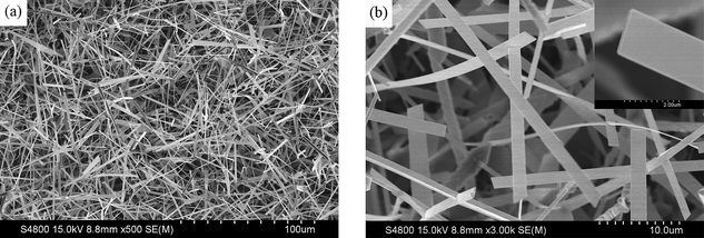 | ||
| Fig. 1 (a) SEM image revealing the high density of Ga2O3 nanobelts. (b) High-magnification SEM image showing the smooth surface and uniform thickness of each nanobelt. | ||
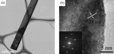 | ||
| Fig. 2 (a) TEM image of an individual Ga2O3 nanobelt, confirming the belt-like structure. (b) Corresponding HRTEM image and inserted FFT pattern demonstrating the single-crystalline characteristics. | ||
Fig. 3a shows a SEM image of an individual Ga2O3 nanobelt device (the following systematic investigation was performed in this device unless a special annotation indicates otherwise). In such a device, the Ga2O3 nanobelt has a width ∼1.6 μm and thickness ∼100 nm. The Ga2O3 nanobelt was connected by Cr/Au electrodes deposited on a SiO2/Si substrate using a standard photolithography process. The right-hand-side inset in Fig. 3b shows a schematic diagram of the device configuration for photoconductive measurements. A monochromatic light was illuminated on the nanobelt in the normal direction, and the I–V characteristics were measured by using the two-probe method. The responsivity (measured current under the unit power density of illumination light) of Ga2O3 nanobelts with different widths is shown in Fig. 3b. It can be seen that the Ga2O3 nanobelt device is insensitive to the light of wavelengths longer than 300 nm. When the wavelength is shorter than 300 nm, the sensitivity increases gradually and reaches a maximum value at about 250 nm, but further wavelength shortening causes a drop in sensitivity. The responsivity at 250 nm is almost 6 orders of magnitude larger than that in the visible light range and this ratio is almost independent of the nanobelt size, indicating high selectivity towards solar-blind light. The appearance of the 250 nm-peak indicates that the photocurrent mainly comes from the electron–hole pairs excited by the light with energy larger than the bandgap. The slight increase of photosensitivity in the long wavelength region (>500 nm) is possibly due to a transition of carriers between defect states in the band gap and the valence or conduction band.32 Defect effects are reflected by the negative photoconductivity under 600 nm light illumination (Fig. 4a). Because 600 nm light corresponds to a very low excitation energy compared with the bandgap of Ga2O3, it can only excite electrons either from the valence band to defect states or from defect states to the conduction band. After a complex excitation and recombination process, the quantity of holes is larger than that of electrons, and thus results in the negative photoconductive phenomenon. Fig. 4b shows a time-dependent photoresponse under different vacuum conditions. In air, the current under light illumination is a little lower than the dark current. When the pressure is decreased to 0.5 Pa, the same phenomenon is observed, but the difference between the dark current and the current under light illumination becomes larger. This is due to the fact that high vacuum reduces the quantity of adsorbed oxygen on the surface of the nanobelt, leaving more free holes for contributing to the photocurrent. The decreased sensitivity at wavelengths shorter than 250 nm is attributed to the enhanced absorption of high energy photons near the surface region of the semiconductor, where the recombination rate of electron–hole pairs is higher than in the bulk.33
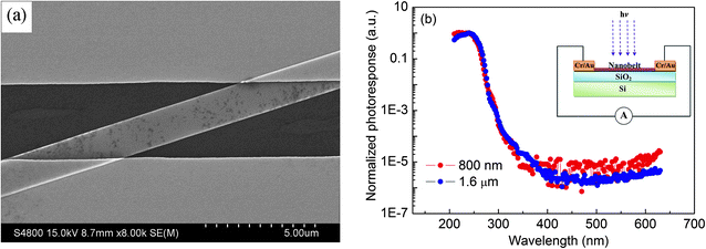 | ||
| Fig. 3 (a) SEM image of a Ga2O3 individual-nanobelt device. (b) Spectral response of the devices (nanobelts with different widths of 800 nm and 1.6 μm) measured at a bias of 15 V. The schematic configuration of a photoconductive measurement is inserted in the top-right corner. | ||
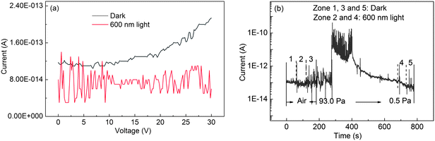 | ||
| Fig. 4 (a) I–V curves of a Ga2O3 individual-nanobelt photodetector under 600 nm light illumination. (b) The photoresponse at a bias of 15 V under air and different vacuum environments. | ||
Fig. 5 shows the time-dependent response of the Ga2O3-nanobelt photodetector illustrated in Fig. 3a, which is measured by periodically turning on and off a 250 nm light at a bias of 30 V. The present photodetector is highly stable and reproducible. The time for the current increase from 10% to 90% of the peak value or vice versa is defined as the rise and decay time (tr and td), respectively. The tr is about 11.8 s, and td is so short that it is beyond the detection limit (0.3 s) of the DC picoammeter apparatus used.
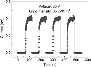 | ||
| Fig. 5 Time response of a Ga2O3 individual-nanobelt photodetector illuminated by 250 nm light with the intensity of 65 μW cm−2 at a bias of 30 V. | ||
Quantum efficiency (QE) is critical for evaluating a photosensitive device, which is related to the number of carriers circulating through a photodetector per absorbed photon and per unit time, determining the efficiency of electron transport and carrier collection. A high QE corresponds to high sensitivity. QE can be expressed by an equation: QE = hcRλ/eλ, in which Rλ is the spectral responsivity (Rλ = Ip/PS, where the photocurrent Ip = Iil − Id and Id is the dark current and Iil is the current of the device when illuminated with a light source, P is the light intensity illuminated on the nanobelt, and S is the effective illuminated area), h is Planck's constant, c is the velocity of light, e is the electronic charge, and λ is the wavelength of illuminating light. The Rλ value of the Ga2O3 nanobelt illuminated by 250 nm light at 65 μW cm−2 is 37.6 A W−1. This corresponds to a QE ∼1.87 × 10².
Fig. 6a represents the I–V curves of nanobelts illuminated by 250 nm light with the intensity varying from 0.72 to 65 μW cm−2. Clearly, the current increases with increasing light intensity. The corresponding dependence at a fixed bias of 30 V is shown in Fig. 6b. This can be fitted well to a power law, Ip ∼ Pθ, where θ determines the response of the photocurrent to light intensity. The fitting gives an almost linear behavior with θ = 0.85. The non-unity (0.5 < θ < 1) exponent suggests a complex process of electron–hole generation, recombination, and trapping within the semiconductor.35 The value of θ = 0.85 suggests that the monomolecular process dominates over the bimolecular process. The device response under the light intensity ranging from 0.72 to 65 μW cm−2 is depicted in Fig. 7a and 7b, from which tr, td, Iil/Id, Rλ, and QE are calculated in Table 1. Dependence of Rλ on the bias is shown in Fig. 7c.
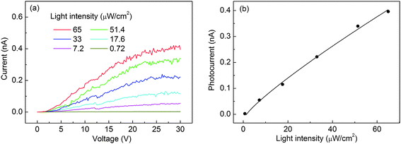 | ||
| Fig. 6 (a) I–V curves of a Ga2O3 individual-nanobelt photodetector under irradiation with 250 nm light at different intensities. (b) Photocurrent as a function of light intensity and corresponding fitting curve using the power law. | ||
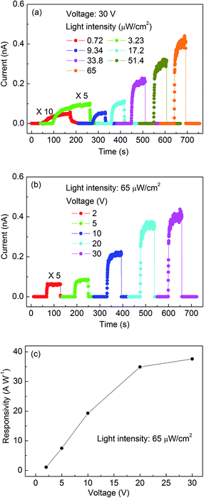 | ||
| Fig. 7 Response characteristics of Ga2O3 individual-nanobelt photodetectors: (a) under various light intensities from 0.72 to 65 μW cm−2 at 30 V, and (b) at a bias ranging from 2 to 30 V under the intensity of 65 μW cm−2. (c) Corresponding responsivity dependence on the bias. | ||
| P/μW cm−2 | t r/s | t d/s | I p/Id | R λ/A W−1 | QE |
|---|---|---|---|---|---|
| 0.72 | 91 | 36 | 1.0 × 10² | 39.2 | 1.95 × 10² |
| 3.23 | 85.8 | 3.3 | 4.0 × 10² | 33.7 | 1.67 × 10² |
| 9.34 | 37.8 | 2.1 | 1.9 × 10³ | 37.8 | 1.87 × 10² |
| 17.2 | 31.5 | 1.5 | 2.7 × 10³ | 37.9 | 1.91 × 10² |
| 33.8 | 21.3 | <0.3 | 5.0 × 10³ | 38.6 | 1.92 × 10² |
| 51.4 | 12.9 | <0.3 | 7.7 × 10³ | 35.1 | 1.74 × 10² |
| 65 | 11.8 | <0.3 | 1.1 × 10⁴ | 37.6 | 1.87 × 10² |
Both the tr and td decrease with increasing intensity, which is due to the distribution of traps in the bandgap of Ga2O3 nanobelts. During light illumination, excess electrons and holes are generated and two quasi-Fermi levels (one for electrons and another for holes) are induced. As light intensity increases, the quasi-Fermi levels of electrons and holes shift toward the conduction and valence bands, respectively, and an increasing number of traps are possibly converted to recombination centers.28 Thus the tr and td are reduced significantly. It is also noted that the tr is much larger than that in conventional bulk semiconductors (<milliseconds) with an intrinsic band-to-band excitation. This indicates that traps and other defect states have also been involved in this dynamic process. The photogenerated carriers may firstly fill traps to saturate them and then reach the maximum number, which induces a delay in reaching the steady photocurrent.
Table 1 lists the QE dependence on the light intensity. It remains almost constant, at ∼1.8 × 10², when the light intensity increases from 0.72 to 65 μW cm−2. Previous results indicated that hole-traps govern the QE and render it independent of the intensity below a critical value. Once the critical intensity is exceeded, the number of available hole-traps is reduced, leading to the saturation and even decrease of the QE owing to the increasing chance of recombination of photogenerated electron–hole pairs.34,35Fig. 7c indicates that Rλ has a nearly linear dependence at a bias <20 V, and tends to saturation at a bias >20 V.
The photoresponse of nanostructures is always affected by adsorption and desorption of oxygen molecules on the surface, and thus it is important to investigate the environment-dependent photocurrent of Ga2O3 nanobelts. Fig. 8a shows the photoresponse of a device under different vacuum conditions measured at a bias of 30 V and a light intensity of 65 μW cm−2. Two major characteristics are obvious: i) The average steady-state current measured in vacuum conditions is higher than that in air conditions. ii) The tr and td increase in the vacuum compared to air.
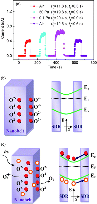 | ||
| Fig. 8 (a) The response of a photocurrent under air and different vacuum environments. (b) Demonstration of oxygen adsorption near the surface of Ga2O3 nanobelts, capturing free electrons in n-type semiconductors. The schematic on the right-hand side is the energy band diagram, revealing the surface band bending and surface depletion area (SDR). (c) Under light irradiation, photogenerated holes migrate to the surface to neutralize electron-capturing oxygen and the remaining electrons migrate to the neutral region. Ev, Ec, and EF denote valence band, conduction band, and Fermi energies, respectively, and red solid and orange hollow circles represent electrons and holes, respectively. | ||
Here the electron–hole spatial separation induced by surface band bending is proposed to dominate the photocurrent, assuming that it is dominated by electrons.29 Under the light-off conditions, oxygen molecules adsorbed on the surface of Ga2O3 nanobelts trap free electrons [O2 + e− → O2−] and thus create surface depletion areas near the surface, as shown schematically in Fig. 8b, decreasing the carrier density and the mobility of the remaining carriers. Upon light-on conditions, electron–hole pairs are generated (hν → e− + h+). The holes tend to move to the surface along the potential slope created by the band bending and recombine with the oxygen-trapped electrons [O2− + h+ → O2]. This results in the desorption of oxygen from the surface (Fig. 8c). After the recombination with holes (produced when oxygen molecules are readsorbed again) the uncombined electrons become the major carriers that contribute to the photocurrent. Upon light-off conditions, oxygen molecules readsorb onto the surface and capture these electrons, which results in a current decay. The increased photocurrent under vacuum conditions is consistent with a longer carrier lifetime owing to less oxygen readsorption in an oxygen-deficient environment.29 The increased rise time is due to the fact that less oxygen adsorption tends to flatten the bending surface band and thus the photogenerated holes on the surface have an increased chance of recombination with free electrons. This leads to a gradual increase of the photocurrent. In the decay stage, fewer O2− results in a slower recombination of electrons and holes, and the photocurrent decreases slowly. The surface trapping process contributes to the sublinear photocurrent–voltage dependence on light intensity.
As shown in the above discussion, band bending usually occurs on the surface of semiconductor nanostructures due to Fermi-level pinning, which results in a recombination barrier of electron–hole pairs. Some reports have shown that the barrier height is related to the nanostructure size.35,36 For comparison, we measured the time response of Ga2O3 nanobelts with two widths, i.e. 3.3 μm (Fig. 9a) and 800 nm (Fig. 9b), The tr and td are respectively about 36 s and 7.8 s for the 3.3 μm-width nanobelt, and both values are less than 0.3 s (detection limit of the apparatus used) for the 800 nm-width nanobelt. These results clearly indicate that a smaller size can produce a faster response speed due to the reduction of the recombination barrier height, which has also been observed in GaN nanowires.35 For 800 nm width nanobelts, the Rλ and QE are calculated to be ∼102 A W−1 and ∼102, respectively. The photoconductive parameters of present and previous works are summarized in Table 2.
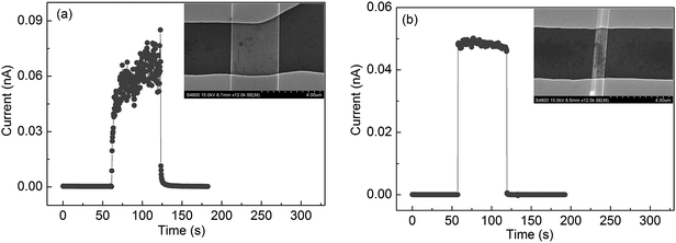 | ||
| Fig. 9 Response characteristics of two different-width nanobelts (a) 3.3 μm and (b) 800 nm under the light intensity 65 μW cm−2 at a bias of 30 V. | ||
Conclusions
In conclusion, DUV solar-blind photodetectors were assembled from Ga2O3 nanobelts synthesized by thermal evaporation in a hot-wall chemical vapor deposition apparatus. The detectors showed high sensitivity and selectivity to light of wavelengths ∼ 250 nm, fast response times (less than 0.3 s), and excellent stability and reproducibility. Functional dependence of the photoresponse on the light intensity, applied bias, measuring environment, and size of nanobelts was studied systematically. A power-law dependence of the photocurrent of Ga2O3 nanobelts on light intensity was determined. Based on the dependence of a response speed (i.e.responsivity) and quantum efficiency on the light intensity, environment, and size of the nanobelts, their photoconductive characteristics were thoroughly understood and the contributions of band bending, surface traps, and trap distribution in the bandgap were uncovered. Ga2O3 nanobelts may find wide optoelectronic applications for photo-sensing, imaging, and optical communications.Acknowledgements
This work was supported by the International Center for Materials Nanoarchitectonics (MANA), National Institute for Materials Science (NIMS), Japan. T. Y. Zhai thanks the JSPS support at the NIMS, Japan.References
- E. Monroy, F. Omnès and F. Calle, Semicond. Sci. Technol., 2003, 18, R33 CrossRef CAS.
- M. Razeghi and A. Rogalski, J. Appl. Phys., 1996, 79, 7433 CrossRef CAS.
- M. Y. Liao, Y. Koide and J. Alvarez, Appl. Phys. Lett., 2007, 90, 123507 CrossRef.
- M. Orita, H. Ohta, M. Hirano and H. Hosono, Appl. Phys. Lett., 2000, 77, 4166 CrossRef CAS.
- K. Koike, K. Hama, I. Nakashima, G. Takada, K. Ogata, S. Sasa, M. Inoue and M. Yano, J. Cryst. Growth, 2005, 278, 288 CrossRef CAS.
- H. M. Huang, R. S. Chen, H. Y. Chen, T. W. Liu, C. C. Kuo, C. P. Chen, H. C. Hsu, L. C. Chen, K. H. Chen and Y. J. Yang, Appl. Phys. Lett., 2010, 96, 062104 CrossRef.
- P. Feng, J. Y. Zhang, Q. Wan and T. H. Wang, J. Appl. Phys., 2007, 102, 074309 CrossRef.
- C. Y. Yan, N. Singh and P. S. Lee, Appl. Phys. Lett., 2010, 96, 053108 CrossRef.
- P. Feng, J. Y. Zhang, Q. H. Li and T. H. Wang, Appl. Phys. Lett., 2006, 88, 153107 CrossRef.
- P. Feng, X. Y. Xue, Y. G. Liu, Q. Wan and T. H. Wang, Appl. Phys. Lett., 2006, 89, 112114 CrossRef.
- Y. Huang, Z. L. Wang, Q. Wang, C. Z. Gu, C. C. Tang, Y. Bando and D. Golberg, J. Phys. Chem. C, 2009, 113, 1980 CrossRef CAS.
- S. P. Arnold, M. Prokes, F. K. Perkins and M. E. Zaghloul, Appl. Phys. Lett., 2009, 95, 103102 CrossRef.
- Y. Kokubun, K. Miura, F. Endo and S. Nakagomi, Appl. Phys. Lett., 2007, 90, 031912 CrossRef.
- N. W. Gong, M. Y. Lu, C. Y. Wang, Y. Chen and L. J. Chen, Appl. Phys. Lett., 2008, 92, 073101 CrossRef.
- L. Fu, Y. Q. Liu, P. A. Hu, K. Xiao, G. Yu and D. B. Zhu, Chem. Mater., 2003, 15, 4287 CrossRef CAS.
- S. I. Maximenko, L. Mazeina, Y. N. Picard, J. A. Freitas, J. V. M. Bermudez and S. M. Prokes, Nano Lett., 2009, 9, 3245 CrossRef CAS.
- G. X. Wang, J. Park, X. Y. Kong, P. R. Wilson, Z. X. Chen and J. H. Ahn, Cryst. Growth Des., 2008, 8, 1940 CrossRef CAS.
- S. C. Vanithakumari and K. K. Nanda, Adv. Mater., 2009, 21, 3581 CrossRef CAS.
- E. Auer, A. Lugstein, S. Löffler, Y. J. Hyun, W. Brezna, E. Bertagnolli and P. Pongratz, Nanotechnology, 2009, 20, 434017 CrossRef CAS.
- (a) T. Y. Wei, C. T. Huang, B. J. Hansen, Y. F. Lin, L. J. Chen, S. Y. Lu and Z. L. Wang, Appl. Phys. Lett., 2010, 96, 013508 CrossRef; (b) J. Salfi, U. Philipose, C. F. de Souza, S. Aouba and H. E. Ruda, Appl. Phys. Lett., 2006, 89, 261112 CrossRef.
- (a) J. S. Jie, W. J. Zhang, Y. Jiang, X. M. Meng, Y. Q. Li and S. T. Lee, Nano Lett., 2006, 6, 1887 CrossRef CAS; (b) M. Law, H. Kind, F. Kim, B. Messer and P. Yang, Angew. Chem., Int. Ed., 2002, 41, 2405 CrossRef CAS; (c) Y. Yao, Y. Liang, V. Shrotriya, S. Xiao, L. Yu and Y. Yang, Adv. Mater., 2007, 19, 3979 CrossRef CAS.
- (a) Q. Wan, E. Dattoli and W. Lu, Small, 2008, 4, 451 CrossRef CAS; (b) R. S. Chen, C. Y. Lu, K. H. Chen and L. C. Chen, Appl. Phys. Lett., 2009, 95, 233119 CrossRef; (c) S. Liu, J. Ye, Y. Cao, Q. Shen, Z. Liu, L. Qi and X. Guo, Small, 2009, 5, 2371 CrossRef CAS; (d) S. Mathur, S. Barth, H. Shen, J. C. Pyun and U. Werner, Small, 2005, 1, 713 CrossRef CAS.
- (a) J. J. Wang, F. F. Cao, L. Jiang, Y. G. Guo, W. P. Hu and L. J. Wan, J. Am. Chem. Soc., 2009, 131, 15602 CrossRef CAS; (b) S. Hinds, L. Levina, E. J. D. Klem, G. Konstantatos, V. Sukhovatkin and E. H. Sargent, Adv. Mater., 2008, 20, 4398 CrossRef CAS; (c) Y. Zhou, L. Wang, J. Wang, J. Pei and Y. Cao, Adv. Mater., 2008, 20, 3745 CrossRef CAS.
- (a) R. S. Chen, S. W. Wang, Z. H. Lan, J. T. H. Tsai, C. T. Wu, L. C. Chen, K. H. Chen, Y. S. Huang and C. C. Chen, Small, 2008, 4, 925 CrossRef CAS; (b) P. J. Li, Z. M. Liao, X. Z. Zhang, X. J. Zhang, H. C. Zhu, J. Y. Gao, K. Laurent, Y. L. Wang, N. Wang and D. P. Yu, Nano Lett., 2009, 9, 2513 CrossRef CAS.
- (a) L. Liao, B. Yan, Y. F. Hao, G. Z. Xing, J. P. Liu, B. C. Zhao, Z. X. Shen, T. Wu, L. Wang, J. T. L. Thong, C. M. Li, W. Huang and T. Yu, Appl. Phys. Lett., 2009, 94, 113106 CrossRef; (b) H. W. Lin, S. Y. Ku, H. C. Su, C. W. Huang, Y. T. Lin, K. T. Wong and C. C. Wu, Adv. Mater., 2005, 17, 2489 CrossRef CAS.
- (a) C. Soci, I. W. Hwang, D. Moses, Z. Zhu, D. Waller, R. Gaudiana, C. J. Brabec and A. J. Heeger, Adv. Funct. Mater., 2007, 17, 632 CrossRef CAS; (b) X. S. Fang, Y. Bando, M. Y. Liao, U. K. Gautam, C. Y. Zhi, B. Dierre, B. D. Liu, T. Y. Zhai, T. Sekiguchi, Y. Koide and D. Golberg, Adv. Mater., 2009, 21, 2034 CrossRef CAS.
- (a) H. Wu, Y. Sun, D. Lin, R. Zhang, C. Zhang and W. Pan, Adv. Mater., 2008, 21, 227; (b) T. Y. Zhai, X. S. Fang, M. Y. Liao, X. J. Xu, H. B. Zeng, Y. Bando and D. Golberg, Sensors, 2009, 9, 6504 CrossRef CAS.
- Y. Jiang, W. J. Zhang, J. S. Jie, X. M. Meng, X. Fan and S. T. Lee, Adv. Funct. Mater., 2007, 17, 1795 CrossRef CAS.
- C. Soci, A. Zhang, B. Xiang, S. A. Dayeh, D. P. R. Aplin, J. Park, X. Y. Bao, Y. H. Lo and D. L. Wang, Nano Lett., 2007, 7, 1003 CrossRef CAS.
- Z. R. Dai, Z. W. Pan and Z. L. Wang, Adv. Funct. Mater., 2003, 13, 9 CrossRef CAS.
- J. M. Blakely and K. A. Jackson, J. Chem. Phys., 1962, 37, 428.
- Z. Y. Fan, P. C. Chang, J. G. Lu, E. C. Walter, R. N. Penner, C. H. Lin and H. P. Lee, Appl. Phys. Lett., 2004, 85, 6128 CrossRef CAS.
- H. Kind, H. Q. Yan, B. Messer, M. Law and P. D. Yang, Adv. Mater., 2002, 14, 158 CrossRef CAS.
- F. Binet, J. Y. Duboz, E. Rosencher, F. Scholz and V. Harle, Appl. Phys. Lett., 1996, 69, 1202 CrossRef.
- R. S. Chen, H. Y. Chen, C. Y. Lu, K. H. Chen, C. P. Chen, L. C. Chen and Y. J. Yang, Appl. Phys. Lett., 2007, 91, 223106 CrossRef.
- R. Calarco, M. Marso, T. Richter, A. I. Aykanat, R. Meijers, A. V. D. Hart, T. Stoica and H. Lüth, Nano Lett., 2005, 5, 981 CrossRef CAS.
| This journal is © The Royal Society of Chemistry 2011 |