Spatially resolved cathodoluminescence of individual BN-coated CaS:Eu nanowires†
Jing
Lin
*a,
Benjamin
Dierre
b,
Yang
Huang
*a,
Yoshio
Bando
a,
Chengchun
Tang
ac,
Takashi
Sekiguchi
b and
Dmitri
Golberg
a
aInternational Center for Materials Nanoarchitectonics (MANA), National Institute for Materials Science, Namiki 1-1, Tsukuba, Ibaraki, Japan. E-mail: Lin.Jing@nims.go.jp; Huang.Yang@aist.go.jp
bAdvanced Electronic Materials Center, National Institute for Materials Science, Namiki 1-1, Tsukuba, 305-0044, Ibaraki, Japan
cSchool of Material Science and Engineering, Hebei University of Technology, Tianjin, 300130, People's Republic of China
First published on 16th November 2010
Abstract
Luminescence properties of individual BN-coated CaS:Eu nanowires have been studied by high-spatial-resolution cathodoluminescence (CL) spectroscopy. A broad red light-emitting band from an individual nanowire has been observed. Detailed local CL studies on the nanowires reveal spatial variations of luminescence from the structure surfaces toward their cores. Such variations are attributed to the different Eu2+ ions surroundings within the surface and core nanowire regions. The attractive luminescence properties are meaningful for fundamental studies of nanoscaled luminescent materials and may be of interest for novel optoelectronic applications.
Introduction
One-dimensional (1D) luminescent nanomaterials are of significant interest owing to their potential applications in nanometre-sized light sources, lasers, fluorescence-labels in biology and optoelectronic nanodevices.1–5 In particular, rare-earth (RE) ion doped 1D nanomaterials have been under active investigation due to the richness of RE ions spectroscopic properties.6Europium doped calcium sulfide (CaS:Eu2+) has been known for many years as a versatile red-emitting phosphor material7 and has potential applications in a wide variety of lighting and display applications, such as field-emission displays (FEDs),8 white light emitting diodes (LEDs)9,10 and electroluminescent devices.11 However, a major drawback of this material is its low chemical stability, even at ambient conditions in the atmosphere. Compared with bulk CaS, CaS 1D nanostructures more easily decompose in air due to their high surface-to-volume ratios. Therefore, the syntheses of CaS-based 1D nanostructures are extremely difficult. Considering the chemical inertness and optical transparency of layered boron nitride (BN),12–14 chemically stable CaS:Eu2+ nanowires can be prepared by coating with a BN protective sheath.15 The BN sheathing layers have been demonstrated to serve as an ultimate protective shield which allow the encapsulated CaS:Eu phosphor to efficiently perform. However, up to now, a challenging study on luminescent properties of individual BN-coated CaS:Eu nanowires has not yet been initiated. It is important to study the local luminescence properties of such complex core/shell heterostructures, not only with respect of the fundamental research on low-dimensional systems but also in regard of their potential applications as interconnectors and active components of future optoelectronic nanodevices.16Cathodoluminescence (CL) is the emission of light as a result of electron bombardment, which is different from the conventional photoluminescence (PL) spectroscopy.17–21 The excitation area during conventional PL is of the order of millimetres, while CL can independently excite a singlenanowire due to its high spatial resolution, up to a few nanometres. In addition, structural information can also be obtained by using secondary electron imaging. On the other hand, one can probe the luminescence behavior of a nanomaterial at different depths from the surface to the core through the use of electron beams with different energies. Therefore, CL is considered as a powerful tool to detect and identify local luminescence properties of individual nanostructures.
In the present work, we have explored the luminescence properties of individual BN-coated CaS:Eu nanowires by employing high-resolution CL spectroscopy. A broad visible red-emission band was observed. The detailed local luminescence studies also showed profound spatial variations of luminescence from the nanowire surfaces toward their cores. Such luminescent properties are envisaged to be valuable for novel optoelectronic nanodevices.
Experimental section
Sample preparation
The BN-coated CaS:Eu nanowires were synthesized in a vertical induction furnace which consisted of a fused quartz tube and an induction-heated cylinder made of high-purity graphite coated with a carbon fiber thermo-insulating layer. A graphite crucible, containing a mixture of CaSO4 (1 g), B2O3 (0.05 g), Eu2O3 (0.012 g) and activated carbon (0.02 g) powders, was placed in the center cylinder zone. After evacuation of the quartz tube to 2 × 10⁻¹ Torr, two pure N2 flows were introduced through the inlets at a flow rate of 1.5 L min−1 (top) and 1.0 L min−1 (base), respectively. Then the furnace was rapidly heated to 1350 °C and kept at this temperature for 1 h. A pink-colored wool-like product was collected after the reaction. For comparison, we also fabricated bulk CaS:Eu without BN coatings. The synthesis process was under the same conditions but without the use of a B2O3 reactant.Characterization
The morphology of the samples was checked by a scanning electron microscope (SEM, JEOL, JSM-6700F). A wool-like product was dispersed in 10 mL alcohol by ultrasonication and then a drop of the solution was dripped on a carbon coated standard Cu grid for characterization in a 300 kV high-resolution field-emission transmission electron microscope (TEM, JEOL, JEM-3000F).CL spectra were measured at room temperature by using an ultrahigh vacuum scanning electron microscope with a Gemini electron gun (Omicron, Germany) equipped with a CL system. The samples were put on a conductive carbon tape and then covered with a copper grid. The vacuum of the chamber was maintained at 10−10 mbar. This prevented the specimen contamination during observation. For CL measurement a beam current was kept at 1 µA and an accelerating voltage (Va) was varied from 1.5 to 7 kV.
Results and discussion
A typical scanning electron microscopy (SEM) image of the as-prepared BN-coated CaS:Eu nanowires is shown in Fig. 1a. High-magnification transmission electron microscopy (TEM) image demonstrates that a single-crystalline CaS nanowire is homogeneously sheathed with uniform BN tubular layers, as displayed in Fig. 1b. More detailed structural and compositional characterization can be found in ref. 15. In order to investigate the luminescence properties of the synthesized BN-coated CaS:Eu nanowires, the detailed CL measurements were carried out at room temperature. Fig. 2a is a SEM image of a representative BN-coated-CaS:Eu nanowire. The CL spectrum taken from this individual nanowire using an accelerating voltage (Va) of 5 kV is shown in Fig. 2c. The spectrum reveals a broad visible emission band centered at ∼660 nm. No other peaks can be observed. We checked numerous nanowires and the results were identical. Fig. 2b is the corresponding CL image, displaying no obvious luminescence difference along the nanowire. The red emission band corresponds to the well-known transitions between the ground state 4f7 and the crystal-field split 4f65d configuration in Eu2+ ions.22–24 Due to the large spatial extension of the 5d wave function and the lattice vibration of the surroundings, the emission spectra from the f–d transitions of Eu2+ are usually broadened.25 The stability of CL was also checked under e-beam irradiation, as shown in Fig. 2d. Under a long time irradiation, the CL intensity shows no notable fluctuations, indicating that the luminescence is relatively stable.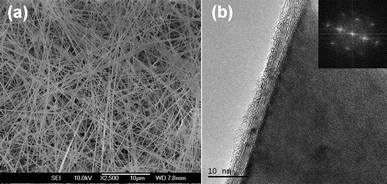 | ||
| Fig. 1 (a) Typical SEM image of the BN-coated CaS:Eu nanowires. (b) HRTEM image and the corresponding Fast Fourier Transform (FFT) pattern (inset) of a nanowire. | ||
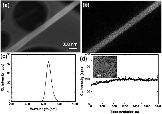 | ||
| Fig. 2 (a) SEM image of an individual BN-coated CaS:Eu nanowire. (b) The corresponding CL image. (c) CL spectrum obtained at 5 kV from the nanowire shown in (a). (d) CL intensity evolutions during the e-beam irradiation at 5 kV. (Inset) The corresponding SEM image. | ||
Then we have also investigated the local luminescent properties of a nanowire. The CL spectra (Va = 5 kV) were recorded within the same nanowire. Fig. 3b plots a number of CL spectra acquired at various locations along the growth axis of the nanowire, as marked in Fig. 3a. The CL spectra are fairly uniform. All peaks are located at the same positions, while the peak intensities are slightly different. Then we collected CL spectra taken at various locations across the nanowire (marked in Fig. 3c). As shown in Fig. 3d, obviously, the CL intensity from the wire core is much stronger than that from its edge. In addition, the peak positions taken in different locations across the wire show an interesting shift. From the edge to the core (from 1 to 3), the peaks have a slight blue shift, while from the core to the edge (from 4 to 7), the peaks have a slight red shift. This result is different from the measurements along the wire growth axis. This suggests that within an individual nanowire the luminescence from the surface and core regions is different. In addition, the spatially resolved CL measurements were also performed across different nanowires. Similar spatial variations of the luminescence were observed (Fig. S1 of the ESI†).
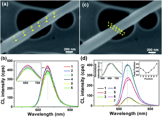 | ||
| Fig. 3 (a) SEM image of an individual nanowire. (b) CL spectra (Va = 5 kV) taken at various locations along the growth axis of the nanowire, as marked in the image (a). (d) CL spectra (Va = 5 kV) taken at various locations across the nanowire, as marked in (c), showing a blue shift from 1 to 3 and a red shit from 4 to 7. | ||
In order to further prove the spatial variation of the luminescence, we measured the CL spectra (Fig. 4a) at various accelerating voltage at a fixed position on an individual nanowire (as shown with a cross mark in the inset SEM image, Fig. 4a; the upper right inset is the Va dependence of the emission peak positions). It also displays a similar shift change. When Va increases from 1.5 kV to 7 kV, the peak positions have a slight blue shift. For the CL measurement, it is known that the lower Va allows exciting the subsurface region of a material, while the higher Va excites the deeper region.18 The reason is that the excitation volume of a lower electron-beam is smaller than the size of a nanowire, while for the higher electron-beam energy, the incident electrons can excite all the regions within a nanowire, including the core (Fig. 4b). Therefore, the increased Va leads to a blue shift of the peak position, which means that the luminescence from the core is blue-shifted compared with that from the surface. This result is consistent with the above-discussed location-sensitive measurements. For comparison, the CL measurement on bulk CaS:Eu without BN coating was also performed. However, with the same Va increase from 1.5 kV to 7 kV, the emission peak positions had no shift (Fig. 4c).
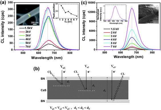 | ||
| Fig. 4 (a) CL spectra taken at various Va at the fixed position on an individual nanowire (seen in the SEM image, inset). The right inset is the Va dependence of the emission peak positions. (b) Schematic illustration of the CL measurements with different Va, indicating that the lower Va allows exciting the subsurface region of a nanowire and the higher Va excites the deeper region. (c) CL spectra taken from a bulk CaS:Eu without BN coating. The corresponding SEM image of the bulk crystal is shown on the inset. | ||
The spatial variation of the luminescence can be attributed to the different Eu2+ surroundings for the surface and core nanowire regions. Fig. 5a shows the structure model of cubic CaS and hexagonal BN within the coaxial heterostructures. During doping, Eu2+ ions prefer to substitute for Ca2+ ions in a CaS crystal lattice due to similarities in ionic radii. Compared with an uncoated bulk crystal, the conditions for the Eu2+ ions at the CaS nanowire surface region are different from the inner ions due to the influence of a BN tubular sheath. Eu2+ usually gives characteristic emission due to transitions between the crystal field components of the 4f65d1 excited state configuration and the 8S7/2(4f7) ground state, which is demonstrated in Fig. 5b. It should be noted that the luminescence of Eu2+ ions is strongly affected by the surrounding environments.22 The emission bands may shift to longer wavelength with the increment of crystal-field strength Δ. Compared with Eu2+ ions in the core, the crystal field strength around the Eu2+ ions within the interface region is stronger, which would enlarge the crystal-field splitting of the 5d level and result in the red-shifted emission.
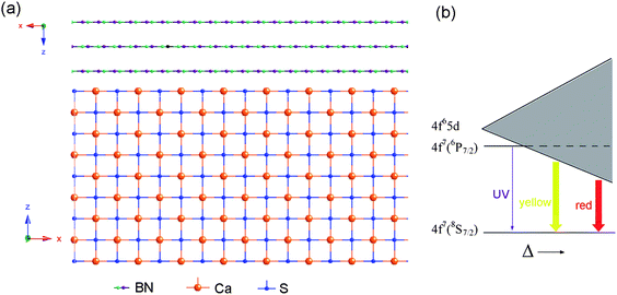 | ||
| Fig. 5 (a) Structure model of cubic CaS and hexagonal BN coating on the nanowires. (b) Schematic diagram of the energies of 4f7 and 4f65d levels in Eu2+ influenced by a crystal field Δ. In most crystals, the lowest excited state of 4f level (6P7/2) is higher than the 4f65d level, so the emission band corresponds to transitions between ground state 8S7/2(4f7) and the crystal-field split 4f65d in Eu2+ ions. The emission will shift to longer wavelength with the strengthening of crystal field. | ||
Conclusion
In summary, we have studied the high-spatial resolution CL spectroscopy on individual BN-coated CaS:Eu nanowires. The nanowires have a broad visible emission band centered at ∼660 nm. Local CL spectra taken across the nanowires display that the luminescence from the nanowire surfaces is red-shifted compared with that from their cores. CL spectra collected at various Va at a fixed position on a nanowire exhibit the same shifts. The spatial variation of the luminescence is attributed to the different Eu2+ surroundings within the surface and core nanowire regions. The attractive luminescence properties presented here are not only meaningful for the fundamental studies of nanoscaled luminescent materials but are also expected to have an effective use in novel optoelectronic nanodevices.Acknowledgements
The authors thank Dr T. Y. Zhai for the technical assistances and kind help. This work was supported by the International Center for Materials Nanoarchitectonics (MANA) of the National Institute for Materials Science (NIMS), Japan.References
- H. Chen, Y. Chen, C. P. Li, H. Zhang, J. S. Williams, Y. Liu, Z. Liu and S. P. Ringer, Adv. Mater., 2007, 19, 1845 CrossRef CAS.
- M. H. Huang, S. Mao, H. Feick, H. Yan, Y. Wu, H. Kind, E. Weber, R. Russo and P. Yang, Science, 2001, 292, 1897 CrossRef CAS.
- X. Duan, Y. Huang, Y. Cui, J. Wang and C. M. Lieber, Nature, 2001, 409, 66 CrossRef CAS.
- Y. Xia, P. Yang, Y. Sun, Y. Wu, B. Mayers, B. Gaters, Y. Yin, F. Kim and H. Yan, Adv. Mater., 2003, 15, 353 CrossRef CAS.
- S. Acharya, U. K. Gautam, T. Sasaki, Y. Bando, Y. Golan and K. Ariga, J. Am. Chem. Soc., 2008, 130, 4594 CrossRef CAS.
- L. Li, C. K. Tsung, Z. Yang, G. D. Stucky, L. Sun, J. Wang and C. Yan, Adv. Mater., 2008, 20, 903 CrossRef CAS.
- W. Lehmann and F. M. Ryan, J. Electrochem. Soc., 1971, 118, 477 CAS.
- M. Leskelä, J. Alloys Compd., 1998, 275–277, 702 CrossRef CAS.
- X. H. He and Y. Zhu, J. Mater. Sci., 2008, 43, 1515 CrossRef CAS.
- D. Jia and X. Wang, Opt. Mater., 2007, 30, 375 CrossRef CAS.
- M. Ando and Y. A. Ono, J. Appl. Phys., 1990, 68, 3578 CrossRef CAS.
- S. Watanabe, S. Miyake and M. Murakawa, Surf. Coat. Technol., 1991, 49, 406 CrossRef CAS.
- O. I. Buzhinskij, V. V. Lopatin and B. N. Sharupin, J. Nucl. Mater., 1992, 196, 1118 CrossRef.
- M. A. Chaudhry, J. Mater. Sci., 1991, 26, 1106 CAS.
- J. Lin, Y. Huang, Y. Bando, C. Tang and D. Golberg, Chem. Commun., 2009, 6631 RSC.
- W. Bu, Z. Hua, H. Chen and J. Shi, J. Phys. Chem. B, 2005, 109, 14461 CrossRef CAS.
- X. L. Yuan, B. Dierre, J. B. Wang, B. P. Zhang and T. Sekiguchi, J. Nanosci. Nanotechnol., 2007, 7, 1.
- B. Dierre, X. L. Yuan, N. Ohashi and T. Sekiguchi, J. Appl. Phys., 2008, 103, 083551 CrossRef.
- B. Dierre, X. L. Yuan, N. Hiosaki, T. Kimura, R. J. Xie and T. Sekiguchi, J. Mater. Res., 2008, 23, 1701 CrossRef CAS.
- U. K. Gautam, L. S. Panchakarla, B. Dierre, X. Fang, Y. Bando, T. Sekiguchi, A. Govindaraj, D. Golberg and C. N. R. Rao, Adv. Funct. Mater., 2009, 19, 131 CrossRef CAS.
- T. Sekiguchi, X. L. Yuan and J. Niitsuma, Scanning, 2005, 27, 103.
- Y. Hu, W. Zhuang, H. Ye, S. Zhang, Y. Fang and X. Huang, J. Lumin., 2005, 111, 139 CrossRef.
- K. N. Kim, J. M. Kim, K. J. Choi, J. K. Park and C. H. Kim, J. Am. Ceram. Soc., 2006, 89, 3413 CrossRef CAS.
- J. Lin, Y. Huang, J. Zhang, H. S. Song, E. M. Elssfah, S. J. Liu, J. J. Luo, X. X. Ding, S. R. Qi and C. C. Tang, Appl. Phys. Lett., 2006, 89, 033118 CrossRef.
- Oh. Knunghwan, T. F. Morse, L. Leinhatr, A. Kilian and W. M. Risen, Jr, J. Non-Cryst. Solids, 1992, 149, 229 CrossRef.
Footnote |
| † Electronic supplementary information (ESI) available: CL images of two different BN-coated CaS:Eu nanowires; CL spectra taken at various locations across the different nanowires. See DOI: 10.1039/c0nr00700e |
| This journal is © The Royal Society of Chemistry 2011 |