Nanomechanics for MEMS: a structural design perspective†
Antonio
Rinaldi
*ab,
Silvia
Licoccia
a and
Enrico
Traversa
c
aNAST center and Department of Chemical Science and Technology, University of Rome “Tor Vergata”, Via della Ricerca Scientifica, Roma, 00133, Italy. E-mail: antonio.rinaldi@uniroma2.it
bInternational Research Center for Mathematics & Mechanics of Complex Systems (MEMOCS), Palazzo Caetani, 04012, Cisterna di Latina (LT), Italy
cInternational Research Center for Materials Nanoarchitectonics (MANA), National Institute for Materials Science (NIMS), 1-1 Namiki, Tsukuba, 305-0044, Ibaraki, Japan
First published on 21st December 2010
Abstract
Nanomechanics and structural design of MEMS are intimately tied together. As mechanical properties of hard materials are found to be strongly sample-size dependent, new criteria are in demand for size-dependent structural analysis and design of MEMS components. The paper offers a critical survey of some of the most interesting and challenging advances in nanomechanics of metals from a MEMS design standpoint. The emphasis is not just on sample size effects in intrinsic properties (in plasticity, elasticity and fracture) but also on extrinsic effects arising in material testing of super hard nano-sized samples and crucially affecting MEMS performance if discarded.
 Antonio Rinaldi | Antonio Rinaldi holds a PhD in mechanical engineering from Arizona State University (2004) and is an Adjunct Professor in the Department of Chemical Science and Technology at the University of Rome “Tor Vergata”. Current research has a strong emphasis on nanomechanics and functional nanoscale materials, within a broader scope that also covers diverse topics in solid mechanics and materials science, e.g. damage mechanics, mechanical design and failure analysis, statistical discrete modeling, microscopy, nanobiotechnologies for health and energy. He is affiliated also with NAST, MEMOCS, ASSOINGE, and INAIL. |
 Silvia Licoccia | Silvia Licoccia is Full Professor of Chemical Foundations of Technology at the Faculty of Engineering of the University of Rome “Tor Vergata”. She is President of AICIng (Italian Association Chemistry for Engineering) and Director of the PhD Program in Materials for Health, Environment and Energy. She coordinates the activities of a multidisciplinary research group comprising research associates, technicians, post-docs and several graduate students. Her activity is mainly focused on the synthesis and characterization of nanostructured materials for energy, environmental and biomedical applications with special emphasis on Polymeric, Solid Oxide and Microbial Fuel Cells. |
 Enrico Traversa | Enrico Traversa is Principal Investigator at the International Research Center for Materials Nanoarchitectonics (MANA) at the National Institute for Materials Science (NIMS), Tsukuba, Japan, leading a group on Nanomaterials for Fuel Cells since January 2009. He joined the University of Rome Tor Vergata in 1988 where he is Professor of Materials Science and Technology. Since 2010 he is Adjunct Professor at Waseda University. His research interests are in nanostructured materials for environment, energy, and healthcare, with special attention to solid oxide fuel cells. He is author of more than 420 scientific papers (more than 270 of them published in refereed international journals). Elected in 2007 in the World Academy of Ceramics, he is currently Associate Editor for the Journal of Nanoparticle Research and Science and Technology of Advanced Materials. |
1. Introduction and general overview
What defines nanotechnology as a whole new technology, and nanoscience as a whole new science, is the dramatic change in the properties of physical systems (e.g. materials) when their dimensions approach the nanometre scale. The prefix “nano” does not merely refer to a small system but bears broader semantic valence and effectively alludes to the novelty of nanoscale physics and its disruptive technological potential. Such a nanoworld needs engineering design to be approached with a new mindset, relying on physical foundations provided by nanoscience. Micro- (MEMS) and nanoelectromechanical systems (NEMS) are a notable example in this regard and represent one of the most active arena of nanotechnology.As far as structural analysis and design of MEMS, challenges arise not just from extreme miniaturization per se, with all it entails in terms of manufacturing and handling limitations, but also from the novel properties that both new and conventional structural materials exhibit on the nanoscale.
Perhaps the most representative instance in this sense is provided by the sample-size dependent mechanical properties of micro- and nano-sized metal samples (e.g.ref. 1–3). This aspect alone implies a profound paradigm-shift in engineering and paves the way to size-dependent design. Conventional structural design, based on the view from classic solid mechanics, holds that both elastic and inelastic properties are generally independent of sample size (at least before the occurrence of severe deformation or any strain localization phenomena) and, hence, relies on bulk properties that can be determined in laboratory experiments from samples of any different size. Conversely, this is not possible in a size-dependent design concept because, in principle, it may be impossible to know a priori—say—strength and plastic properties of a given metal unless either ad hoc testing is carried out for a completely specified configuration (e.g. giving size, geometry, shape, load configuration, other physical conditions, etc.), or an applicable scaling law exists to infer the materials properties from one scale to another.4
The study of such sample-size effect falls in the domain of nanomechanics, which is that branch of nanoscience that studies mechanical properties at large of nanoscale materials. As such, it provides nanotechnology with the knowledge needed, in particular, for structural design of MEMS and nanosystems, i.e. those having relevant nanoscale components. Historically the advent of nanomechanics as an actual nanoscience was fostered by the invention and eventual refinement of scanning probe microscope (SPM) technology (e.g.ref. 5 and 6), which only in the past 10–15 years reached the sufficient advancement to enable well controlled mechanical testing on the nanoscale, not just of thin films but of individual nano-sized material samples too. With time, nanomechanics has become a booming research field where scientists, thrilled with the newborn possibility of a direct access to nanoworld information, have dedicated an ever growing amount of work to the characterization of all sorts of elementary nanostructures made of many different materials, both single phase and nanostructured/nanocomposite ones, shaped in different guises (e.g.nanoparticles, nanopowders, nanowires, nanoribbons, nanotubes, nanoshells, nanomembranes, etc.). The leitmotif of this experimentally driven effort has been the disclosure of the characteristic deformation mechanisms of materials at the nanoscale. Yet this activity has been done somewhat erratically with custom made set-ups and procedures that differed considerably across groups worldwide and over time (e.g.ref. 3 and 5). In this respect, a trained-eye cannot fail to appreciate at a glance the greater accuracy of test data from a recent micro-compression test on a nanoparticle or on a nanopillar in comparison with the early days. This improvement is the result of increasingly higher control over the contact geometry during testing, which was spawned by a febrile and fertile gold-rush to deliver new testing equipment and sample preparation protocols that rapidly superseded previous ones. For instance, the advent of TEM-monitored nanomechanical testing in recent years marked a point of no-return that made look obsolete other set-ups developed just a few months earlier. Due to such a high degree of dynamism, today nanomechanics has a clear footprint but, despite the remarkably fast scientific growth, is far from being an established science with robust metrological foundations. The lack of much needed technical standards in nanomechanics, let alone ISO 14577 and ASTM E2546 about micro- and nanoindentation, is a meaningful indication of this gap, proving that nanomechanical testing is still an unconventional and young approach, about which there is still insufficient or controversial knowledge—on top of conflicting commercial interests. Issuing standards on data collection and analysis in nanoscale testing is evidently critical to produce the reliable information for size-dependent design of MEMS and is a top research priority.
Besides fast technological obsolescence, other aspects are relevant by a metrological standpoint and need to be addressed to draft standards. The compliance of text fixture in nanoscale experimental set-ups is one important example and is exquisitely a nanometre scale problem. Because nano-sized materials may exhibit much higher hardness than conventional samples, the deformation of the fixture becomes relevant and gives origin to some extrinsic effects in the test response.7 Nanoscale extrinsic effects cannot be treated like in conventional testing (e.g. by oversizing test samples with respect to contact zones with fixtures) and distinguishing the actual property of the material (i.e. the intrinsic behaviour) from the artifacts (i.e. extrinsic effects) in test data is presently a major challenge in nanoscale testing and metrology. Furthermore, as the sample size continues decreasing, the study of extrinsic effects is doomed to become central in nanomechanics and in the development of better equipment, on a par with intrinsic material properties.
The importance of nanomechanics to MEMS design cannot be overemphasized. Even though many commercial finite elements software packages are flexible design tools and already feature adds-on modules specific to MEMS, it will be nanomechanics to supply the correct constitutive models of materials at the length scale relevant to the design, as fabrication techniques improve and MEMS components shrink in size. Furthermore, understanding and controlling the intrinsic and extrinsic nanoscale effects are necessities not just for the structural analysis and design of any MEMS (and NEMS), but in particular for the functional design of some MEMS sensors and actuators, such as the force sensing device in Fig. 1. The 3D force transducer MEMS shown therein features an advanced design that allows for a full measure of small point forces applied at the tip of a cantilever (performance and design to be examined in a separate manuscript).
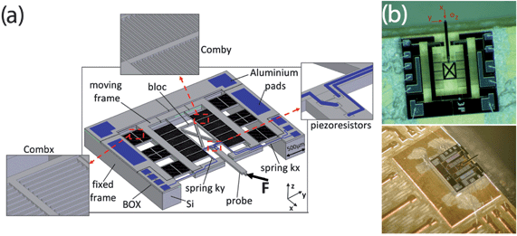 | ||
| Fig. 1 3D MEMS force transducer. (a) The montage shows a CAD model with insets showing CAD micrographs of key structural area and the electrical scheme of the device. The working principle for the 3D is explained next. The force components Fx and Fy applied at the tip of the cantilever probe cause the displacement in x–y of moving comb fingers, inducing capacitance variations. Fz is instead resolved by piezoresistors implanted on the probe-end restraint sensor and actuator for x and y directions (electrostatic actuation—combs). The decoupling between directions is achieved by a careful choice of the piezoresistors locations and adjustable springs configuration, such that the force range is easily tuned to fit a given application, i.e. mostly by adjusting the springs dimensions made from n-type SOI wafer. (b) Photos of the actual prototype. The width of the sensing cantilever is about 150 µm (credit: courtesy of J. Verstraeten, P. G. Charette and V. Aimez, CRN2, Université de Sherbrooke, Qc, Canada). | ||
2. Intrinsic material properties
2.1. Plasticity
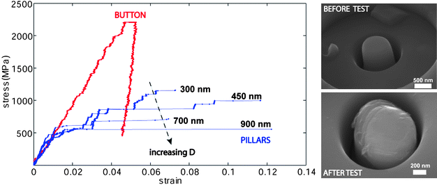 | ||
| Fig. 2 (left) Representative stress–strain curves of pillars of different diameter D and of a short pillar with D ≈ 200 nm and h/D ≈ 0.6 (labeled as “button”). The pillars show the well-known size dependent plasticity, with incipient slip events starting at around 500 MPa and ultimate strengths over 1 GPa for D ≈ 300 nm. On the other side the button exhibits a distinct response, nearly linear during loading up to the maximum load and without failure. (right) SEM micrographs of a pillar with D ≈ 900 nm before and after testing, showing a structural failure by shear localization. | ||
By now this phenomenon has been confirmed a number of times and well described in many specialized publications, which have been recently summarized in a focus review on single crystal metal pillars.3 In fact, most work was done on single-crystal plasticity, mostly on FCC metals (e.g.Ni, Au, Al, Cu, etc.) for simplicity sake, due to their propensity towards single slip deformation as the main failure mode.10 However, the interest in single crystals is timely and advantageous for mechanical design because single crystal materials, conventionally reserved for special applications (e.g. aerospace), are going to be potentially more pervasive and widespread in MEMS design and nanotechnology than in classical engineering. Also, what makes the results from pillars experiments particularly valuable from an engineering perspective, as compared to previous observations of the size effect by Brenner and others, is that the flow stress σy (here representing the sample strength) was proved for the first time to scale with D in a fractal fashion, according to a power law
| σy ∝ D−β | (1) |
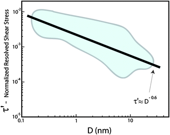 | ||
| Fig. 3 Log–log plot of the universal scaling law (as offered in ref. 3) for the normalized resolved shear stress τ′ = a(τ/G)of a target metal where τ = σySF is the resolved shear stress on the active slip plane in the test computed as τ = σySF through the proper Schmid factor (SF), G is the anisotropic shear modulus and a = bref/bmental is the ratio between the Burgers vector of a reference (“ref” stands for Ni here) and the target. The regression line suggests an approximate universal exponent β ≃ 0.6 and is plotted over the envelope of the experimental data considered in the regression to offer also visual information about the sensible data spread. | ||
Theoretical relations such as scaling law (1) are the kind of nanomechanical results needed to curb our dependence on experimental characterization of materials and establish size-dependent structural design principles for MEMS. For engineering purposes, it is also fundamental quantifying and scaling the variability as a function of size, although the scaling law (1) presently just refers to the mean response. The envelope of experimental data points, plotted in Fig. 3, illustrates that variability may indeed be large. The pillar data in Table 1 point out that the data scatter measured as standard deviation of flow stress appears to increase as D reduces, which is a non-trivial aspect that has received little attention by the materials science community but needs to be investigated for engineering sake.
The size effect in pillars should disappear once D reaches the point where size independent bulk properties are restored. It is still unclear when this transition happens and specific experiments are ongoing. Current data indicate that the D-dependence is certainly active for pillars of a few tens of micrometres and, not without surprise, even in microcrystals as large as 80 µm. This indication is sufficient, though, to appreciate the importance of size-dependent structural analysis principles for MEMS and NEMS (not just for crystalline metals as seen later).
Although most of the work in pillars plasticity has focused just on D-dependence, D is not the only relevant parameter. The authors of this paper and their co-workers have recently demonstrated that also the height h plays an important role7 because it can constrain crystal plasticity all together if lowered beyond a theoretical threshold dependent on crystallographic orientations, which results in ultra-strong nanostructures. Fig. 2 shows the comparison between ordinary pillars and a short pillar (D ≈ 200 nm and h ≈ 120 nm) of the same material, labeled button for distinction (see ref. 7 for exact definition). The button sustained stresses greater than 2 GPa and behaved nearly linearly during loading up to the maximum applied load without failure. The actual compressive strength of the buttons remains unknown but could be tremendously higher considering a theoretical limit value of order of 20 GPa for compressive strength (∼G/π) of a defect-free Ni crystal. In this case, the effect of D is totally prevented by the h-induced strengthening effect, which—unlike the D effect—does not vary continuously with h but is an on–off phenomenon caused by a point-transition in the deformation mechanism. The underlying idea is that the button represents a load configuration where all active slip systems intersect the base of the pillar, which acts as a kinematic constraint and literally block free plastic slip. While this type of issue is known on the macroscale but can be avoided in conventional design by recurring to the Saint-Venant's principle, it is important to acknowledge that nano-sized materials can have dramatically different response depending on shape and (internal or external) constraints, especially for the design of MEMS and NEMS components with complex shapes. Evidently this extra strengthening mechanism can be exploited to the designer’s advantage to boost mechanical performance.
Another aspect relevant to MEMS structural design is the mechanical anisotropy of single crystals. Crystal orientation and symmetry affect both the elastic and plastic properties of the material. While conventional knowledge of elastic anisotropy is expected to hold on the nanoscale, the effect of crystallography on nanoscale plasticity is more controversial and represents an open research subject, largely unexplored. The two stress responses plotted in Fig. 4 were obtained from ancillary experiments performed in our group on pillars (D = 300 nm) with different crystallographic orientations to appreciate the considerable difference in the plastic response that can result. While the pillar “A” appears much stronger and shows a smooth response, the pillar B begins yielding much earlier and to a greater extent but exhibits a different shaped response, alternating elastic loading and discrete plastic events. The latter scenario is often encountered in nanoscale plasticity and represents a major difference with respect to the conventional behaviour. The intermittent plasticity of pillar “B” indicates that plasticity is a random process that can start at a random stress level and immediately stop. This characteristic type of behaviour is not well described by conventional strain hardening models developed for continuous plasticity and found in most finite element codes.
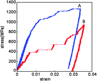 | ||
| Fig. 4 Stress response of two 300 nm single crystal Ni pillars with different crystallographic orientations (materials were prepared and FIB machined in identical ways). Compression tests were performed with a Berkovich tip. Crystallography plays a key role in the crystal response, which for pillar A renders a continuous plastic response (similar to conventional macroscale observations) but for pillar B determines an intermittent plastic response, where discrete plastic events happens in between elastic segments. The latter behaviour is often encountered in nanoscale crystal plasticity. | ||
The size-dependent strengthening and all the other concepts illustrated for FCC crystals need to be characterized more thoroughly for BCC crystals, where the mechanics is more complex because plastic deformation proceeds not just by single slip but by twinning too, as confirmed recently via electron backscattered diffraction (EBSD) during TEM-monitored tests of molybdenum (e.g.ref. 3 and 11). Pillar testing is being deployed also for other engineering materials, such as metallic glasses, intermetallics, superalloys, shape memory alloys, and nanocrystalline metals, which represent more difficult systems and are now being investigated very actively by means of the pillars methodology, as recalled in ref. 3.
Nanocrystalline metals (i.e. metals with nanosized grains) are, for example, still rarely encountered but may have superior properties compared to single crystals. In fact, based on our own experience, polycrystalline Ni pillars with diameter of ∼200 nm and ∼300 nm and an average grain size of ∼20 nm displayed a visible sample size effect with a scaling exponent β = 0.66, as shown in Fig. 5.2 In comparison to the single crystal counterparts (Fig. 2), the stress flow of these pillars is much higher, with less ductility and pronounced strain hardening. This super-hard material indicates that controlling the grain size provides yet another strengthening mechanism at the nanoscale, an extensive characterization of which is still unreported.
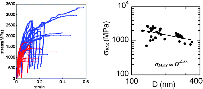 | ||
| Fig. 5 (a) Compression stress–strain curves for the two sets of nanocrystalline Ni pillars examined, 24 samples at 160 ± 30 nm (red) and 15 samples at a diameter of 272 ± 30 nm (blue). (b) Double logarithmic plots of yield strength (or maximum stress sustained in the test) versus pillar diameter showing power-law behaviour in compression. | ||
In the past 2–3 years the direct observation of dislocation evolution in nanomaterials by TEM observations broadened enormously the understanding of structure–property relations in nanoscale effects and produced a few new theories. In the first place it was proven that not only a considerable number of initial dislocations could stably reside in a pillar shaped crystal as small as 50–200 nm, but, upon applying a compressive load, many of them would egress out to the surface rather than multiplying. Reportedly a 〈111〉 Ni crystal smaller than 200 nm could become defect-free by this process, whereas a residual density of dislocations would still persist in larger crystals after a compression as high as 2.6 GPa.14
This phenomenon was named mechanical annealing, evoking a load-mediated transition to a more ordered, defect free nanostructure of superior strength (confirmed by subsequent re-compression). Other studies, though, demonstrated that mechanical annealing does not always happen and is not the only mechanism that could explain strain hardening plasticity. An interesting example is provided by the composite nanoparticle (CNP) shown in Fig. 6, consisting of a ∼130 nm amorphous core of transition metal cobalt boride covered by a ∼10 nm silica outer layer. This material is evidently highly disordered from the start as a distribution of radial defects can be observed in the cobalt boride core.15,16 Once tested in compression the CNP proved to be much harder than bulk material and to undergo a considerable strain-hardening. This was evident because, after applying a sustained load, the CNP response became harder and practically elastic in subsequent loading cycles.
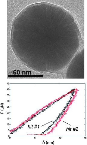 | ||
| Fig. 6 (a) TEM analysis of a 150 nm CNP characterized by a ∼10 nm thick silica shell coating the magnetic Co2B core of ∼130 nm. Radial defects exist in the core of transition metal cobalt boride (credits: V. Salgueirino-Maceira, Univ. Vigo). (b) Repeated compression tests on a target CNP unveiled special plastic effects such as reverse plasticity at moderate loading range. | ||
The occurrence of traditional strain hardening on the nanoscale is in itself a novelty, countering mainstream thinking. As this work was not done in a TEM environment we could not see the evolution of the initial radial defects but we can exclude a mechanical annealing type of mechanism here in favor of a more conventional strain hardening mode based on, e.g., defect interaction, multiplication, and trapping, producing an increase in the inner disorder.
Another interesting aspect of nanoscale plasticity is that it ceases to be necessarily an inelastic phenomenon. This apparently nonsensical statement refers to the existence of the so-called reverse plasticity,15–19 a nanoscale phenomenon consisting of the recovery—perhaps after some time—of the plastic deformation from testing once the load is removed. From a MEMS design standpoint, this phenomenon is unconventional and represents a source of non-linearity and time-dependence in the constitutive model of the material, which may perhaps be treated as a nonlinear visco-elastic effect as a first approximation. Reverse plasticity has been clearly observed in nanoparticles but is not yet completely understood. Its dependence on sample shape, for instance, is not known, as well as the transition to the truly inelastic regime by means of the above mentioned strain hardening mechanisms. The inelastic deformation, though, requires relatively larger stresses as reverse plasticity was mostly observed at low loads in compression tests of nanoparticles.5,18,19 What is particularly puzzling is the occurrence of reverse plasticity both in single phase, ordered nanoparticles and in disordered systems such as the CNP.15,16 The two repeated tests on a CNP shown in Fig. 6(b) demonstrate that the plastic deformation caused by hit #1 was recovered (confirmed viaAFM scanning) and that the CNP response measured from hit #2 replicated, in practice, the first test. If the compression exceeded 40 µN the inelastic mechanisms described above got activated.
As a final remark, several research groups have pointed out that changes in mechanical responses of nanosized materials may likely stem from deformation mechanisms based on phase transitions. The study of phase transition deformation by means of high-resolution techniques (e.g.TEM, SPM, ab initio calculations)20,21 is indeed a very interesting research topic in nanomechanics, especially in non-FCC crystals (not covered in the present review for brevity).
 | (2) |
| F(σ;V) = F(σREF;VREF) | (3) |
 | (4) |
 | (5) |
 | (6) |
 | (7) |
This theory is derived here with reference to single crystal plasticity just for the sake of argument but it is applicable to other random nanomaterials as long as m can be linked to that type of disorder. As a matter of fact, this theory was first formulated and validated by our group on nanocrystalline Ni (Fig. 5).2 In that study, we additionally speculated that the yield stress could scale with the pillar surface S = πDh rather than V, depending on whether surface defects or volume defects governed the physics of plasticity in such a polycrystalline material. From a mathematical standpoint24 this is equivalent to admit that for a surface controlled phenomenon the modulus could be
 | (8) |
In principle, if both types of defects are relevant, eqn (7) and (8) could just represent upper and lower bounds for m respectively and could be used to discriminate what defect type plays a bigger role, based on whether the actual value falls closer to one or the other bound. For data in Fig. 5, referring to β = 0.66, the bounds would be 3 and 4.5.
For validation, a direct estimate of m is sought from the data in Fig. 5 by fitting a Weibull distribution (with the maximum likelihood method) to the experimental histogram of yield stresses of pillars from a subset of pillars with same size. In Fig. 7, fitting a Weibull distribution from 24 nanocrystalline pillars with D < 200 nm25 proves to be reasonable, as confirmed by the probability plots (b), and renders an estimate m ≈ 3.4. This appears to be a plausible value, well within the predicted range 3–4.5 and closer to the indirect estimate from eqn (8) (i.e.m ≈ 3), which lead us to speculate that surface defects may dominate the plasticity of nanocrystalline pillars. The agreement is particularly satisfactory and encouraging in consideration of the simplicity of the deployed arguments, which nonetheless requires an extended validation to rule out chance and fine tune the approach. More work is currently being done on this material by other groups too (e.g.ref. 26).
 | ||
| Fig. 7 (a) Histogram of flow stresses as measured from 24 compression tests of pillars with D ≈ 200 nm and fitted Weibull distribution (line). (b) Weibull probability plot with 95% confidence interval indicates a good fit with P > 0.25 for data from Fig. 5a. The modulus m ≈ 3.4 correlates well with indirect estimate eqn (8) from scaling exponent β = 0.66. | ||
The pursuit of structure–property relations is of practical importance for structural design of MEMS components because on one side it complements the experimentally observed scaling laws, such as eqn (1), and on the other side opens the door for tuning such a scaling law (and the plastic phenomenon) through the engineering of the nanostructure and the control of type and amount of disorder. This discussion puts in evidence that, besides sample size dependent effects per se, the designer needs to know content and type of disorder, which depend on the processing history (e.g. thermal treatments, FIB-machining, other microfabrication techniques, etc.), to assign correctly the proper engineering properties to a material.
Manufacturing techniques are responsible also on the nanoscale for residual stresses and inner disorder of the microstructure, as observed in Si micropillars by means of sophisticated white beam Laue diffraction experiments.27
2.2. Elasticity
The elasticity of nanomaterials has drawn much less attention than plasticity but it is very important to structural design of MEMS. As a matter of fact nanotechnology has determined a revival of elasticity theory because all the strengthening mechanisms discussed above, in particular the plastic sample-size dependent strengthening, meant an equal extension of the elastic regime as sample-size reduces. Furthermore, because single crystal materials are frequently used in MEMS, the relevance of anisotropic elasticity is particularly poignant to nanoscale design, in contrast to the traditional structural engineering relying most often on the isotropic case.28The phenomenology of nanoscale elasticity presents also some characteristic traits interesting for advanced structural design. One of these aspects is the stiffening of the material observed in nano-sized samples subject to compression. In the conventional view, the Young modulus E0 in ambient conditions (and bulk elastic tensor in general) is a constant parameter measurable experimentally by tensile or compression tests or by wave propagation methods. However, compression tests on single phase nanoparticles in the 40–140 nm diameter range pointed out that the elastic modulus may tend to increase under applied pressures of order of GPa, measured in those specific experiments as the ratio of the applied load to the estimated contact area of the nanoparticle. In particular, Mook and coworkers5 proposed that a linear relation (inspired by a prior model used in geology for a similar effect in highly constrained rocks and diamond anvil cells) between the Young modulus and the pressure p
| E(p) = E0 + β(p) | (9) |
 | ||
| Fig. 8 Dependence of Young modulus E on the applied pressure p for the button from Fig. 2. The modulus was computed from the unloading path. Values much higher than bulk Ni are recorded at maximum load, which decay quasi-linearly as the pressure level drops below 1 GPa. Values lower than conventional Ni, away from the stress peak, are not reliable. | ||
From a design perspective, since the stiffness is the single most important parameter in elastic design (also in dynamics applications), the stiffening effect bears implications. Even though it has to be investigated for tensile loading too, the reported findings suggest that discarding such non-linearity in favor of standard elastic constants may underestimate, for example, the real stiffness of nanoscale components bearing compressive loads. Consequently, this type of non-linear elasticity is expected to be added, at some point, to the capabilities of commercial FEM codes for MEMS design.
2.3. Toughness and fracture behaviour
A considerable amount of work in this area has been done on thin-films since the '90s.29 However, as far as in situ testing of nano-sized materials (e.g. pillars or particles), a modern nanoindenter can be used to nucleate a crack in such samples but research lags behind in comparison to plasticity and no systematic work has been undertaken or reported yet. In this regard it is noted that published papers addressing fracture properties of nanostructures are a tiny fraction of those on plasticity. This is partly due to objective technological limitations in testing equipment that prevented, for example, to perform tensile testing on sub-micrometre pre-notched samples for a long time. The micro-compression tests that indeed dominated the experimental scene in nanomechanics over the past decade are very effective for plasticity but are not an optimal setting to study material fracture and toughness. The situation is doomed to change as novel nanoscale testing is being introduced (e.g.ref. 12,26,30 and 31) and microfabrication techniques enable increasing control over defects and shapes, eventually allowing machining (or fabricating in general) nanosized sample geometries containing nanocracks and optimized for crack testing. It is worth recalling that fracture properties are as crucial to the design of brittle materials as plasticity is for ductile systems. It is our opinion that the study of fracture properties (along with fatigue and creep properties) at the nanoscale may likely be the next booming area in nanomechanics for the coming decade.Furthermore, the preliminary exploration done so far on nanoscale metals promises the existence of strong and interesting size effects in nanoscale fracture. One effect of utmost importance is the switching from ductile to brittle behaviour or vice versa. For example, silicon (a FCC metalloid) is known to be a brittle material in engineering but at the nanoscale it acquires a ductile character, as revealed by in situ testing of individual Si nanostructures. This effect was first observed in compression tests of Si nanoparticles of 40 nm in diameter, which showed a fracture toughness estimated to be four times as much that of the bulk and appeared to indicate the stress intensity factor KIC to vary as 1/d.5,29 However, a complete shift in failure mode was observed only recently in tests of nanopillars.32 As outlined schematically in Fig. 9, a ductile-to-brittle transition appeared to happen for D below a threshold around 300–400 nm. Below this value the Si pillar exhibited a higher strength and failed plastically, just as Ni and other FCC ductile metals. Instead, above the threshold, the pillars underwent splitting, which is a failure mode typically observed in brittle materials subject to compression (e.g. concrete) and consisting of the formation of a crack along the compression axis. In the latter case, as depicted in Fig. 9(b), the combination of compression and frictional adherence between the indenter flat tip and the pillar top determines a highly constrained conical zone that, acting as a wedge pushed downward by the indenter, split-cracked the Si. Unfortunately, because such a cracking mechanism relies on boundary effects and apparently does not work for ductile materials, it does not provide a general methodology to measure the toughness of nanoscale materials. Yet, these observations convincingly demonstrate ductility in Si.
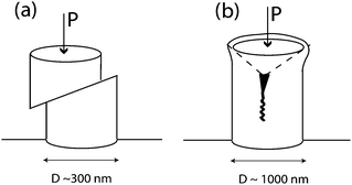 | ||
| Fig. 9 Schematics of brittle-to-ductile transition controlled by D in single crystal FCC Si pillars (drawn after ref. 29). (a) Ductile behaviour below the transition in a 300 nm pillar failing by single slip. (b) Brittle behaviour in a 1 µm pillar failing by a split crack induced by the wedge-like action of the incumbent deadlock cone of material. | ||
The reported effect is not conclusive by any means, also because the inverse transition has been argued to occur in other ductile materials, such as gold. In fact, a previous study on nanoporous Au consisting of a percolating sponge-like network with controlled ligament size showed that the fracture strength obtained from three point bending tests increased as the average ligament size reduced from 1 µm down to 10 nm and that the type of failure became suddenly brittle for the nanometre sized sample.33
The brittle nature of nanoporous gold can be appreciated in the crack from Fig. 10, where there is no obvious hint of dimples or ductility. The dichotomy between the ductile-to-brittle transition in Au and the opposite phenomenon in Si, although in different experiments, testifies the need for a focused effort in nanomechanics to address and sort out fracture issues.
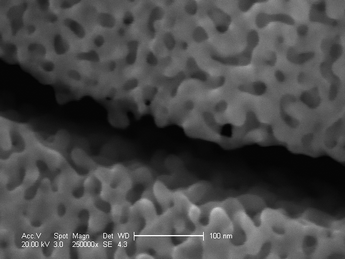 | ||
| Fig. 10 Crack in a nanoporous gold (obtained from a Au30Ag70) showing no obvious sign of ductile failure in the 10–20 nm ligaments. | ||
Aside from static problems, another topic crucial to MEMS design is represented by fatigue fracture. A substantial amount of work has been done already, particularly on polycrystalline Si, which is key to MEMS. Its limited damage tolerance exposes Si to crack initiation and subcritical crack growth, eventually leading to brittle failure. This was ascertained experimentally on micro-sized Si specimens by several researchers (e.g.ref. 34–36), finding, for example, a reduction of the static strength greater than 30% after 108−9 cycles. Other materials have been targeted, such as Pt, Ni and Ni–Fe nanosized microstructures and some modeling attempts have been also proposed (e.g.ref. 37). The mechanistic origins, as well as both strengthening and weakening mechanisms, are a theme of continued investigation from scientific and industrial standpoints (for detailed discussion of this topic, refer to the cited papers).
3. Extrinsic effects in nanomechanics
Extrinsic effects, collectively, refer to the bias in experimental data coming from effects at the boundary or, anyways, outside the material sample. On the nanoscale they represent a serious issue and devising ways to get rid of them is in order to obtain the right stress–strain relations for structural design and to insure the correct functionality of strain sensing MEMS. Because many extrinsic effects arise with metals and other hard materials, the design of MEMS devices for testing soft materials is less demanding in this respect. Fig. 11, for example, shows a MEMS device for tensile test of individual polymer fibers that are gripped by FIB sputtered material, a solution unfeasible with metal samples of similar geometry requiring much firmer grip. Extrinsic effects in hard materials have many origins, some of which are discussed next.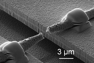 | ||
| Fig. 11 MEMS device to test individual polymer microfiber. A single fiber fractured is shown (credit: ©Fraunhofer IWM—Jaeger et al. (2009)). | ||
3.1. Extrinsic effects from elastic phenomena
The substantial strengthening observed in micro- and nanosized metal samples represents a criticality in terms of extrinsic effects. As a material becomes harder, the sample exchange greater tractions with the surroundings and the applied load may rise to the point that fixtures undergo a non-negligible deformation, which is usually undetected in the experiment and confounded with the material response. In the pillars experiments, for instance, the raw stress–strain datasets need to be corrected to remove the contribution of the elastic deformation of the compliant foundation from the measured strain, also known as Sneddon effect.3,6,7 According to Sneddon, the overall displacement ΔXtot and the actual contribution ΔXpillar of a pillar subject to uniform compression are related through the aspect ratio AR = h/D and the Poisson ratio ν28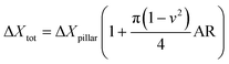 | (10) |
Then, the fraction of the deformation associated to the foundation corresponds to
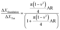 | (11) |
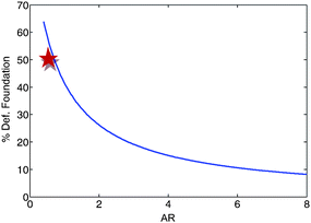 | ||
| Fig. 12 Plot of percent deformation attributed to the (elastic) foundation out of the total deformation measured in pillar experiments as a function of the aspect ratio AR = h/D of the pillar according to eqn (11). The star marks the value for the button in Fig. 2. | ||
The contact asymmetry at the top and bottom of the pillar is itself a challenging aspect because it implies different fixtures conditions at the two ends, which is carefully avoided in conventional macroscale experiments but not easily at the nanoscale.
A similar scenario holds for nanoparticles, which are often tested in compression between a diamond platen and a softer (often Si) fixed substrate. The Oliver-Pharr method15,38 is used to analyze test data, accounting for the compliant fixture in a manner effectively analogous to the Sneddon correction.
3.2. Extrinsic effects from inelastic phenomena and other sources
Besides elastic compliance, fixture materials may experience also inelastic deformation, especially plasticity. Considering even a metal pillar undergoing mechanical annealing and becoming stronger during loading, it is reasonable to expect the foundation made of the corresponding bulk metal to be the weakest element in the compression experiment. Based on our observations on super-hard buttons,7 the measured response presents indeed several signs of extrinsic phenomena. When comparing the two button tests in Fig. 13 (inset), the two stress–strain responses display a striking agreement up to about 1 GPa and then depart from each other due to a series of visible plastic slips of different magnitudes. These slips cannot relate to crystal slip since generalized crystal plasticity is constrained in these samples, as explained earlier.39 These “bursts”, instead, do not occur at random but orderly, in a systematic pair-wise fashion at defined stress ranges in both buttons; paired slips on the two curves are pointed out with arrows in Fig. 13. This circumstance is really a clue of an underlying extrinsic effect, which at present could only be detected but not fully understood. On the one hand, such ordered slips may simply relate to the plastic deformation in the compliant foundation; after all, the Sneddon correction applied in Fig. 13 only removed the elastic component of the foundation strain, leaving untouched any inelastic artifact. Alternatively, we cannot exclude these slips to result from gradual “engaging” between the tip-platen and the top of the button since the roughness of the contact surfaces and the difference in hardness of diamond and Ni are likely dislocation sources. In either case, slips in Fig. 13 are not an intrinsic button property but extrinsic bias from plastic events happening at the button ends or externally, which can be removed (as explained in ref. 7) once diagnosed.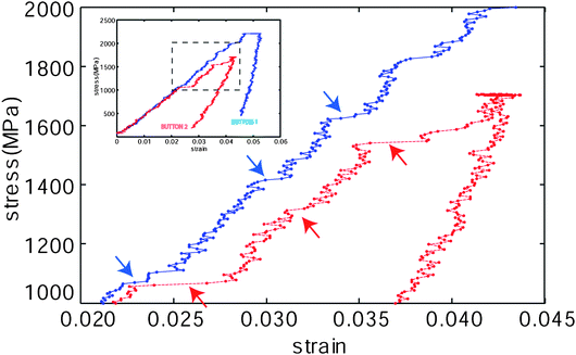 | ||
| Fig. 13 Caption responses of two buttons of same size (i.e.D and AR) loaded up to 2 GPa (blue) and 1.7 GPa respectively (red). After 1 GPa, the responses deviate from each other due to plastic events of different magnitudes but happening at rather determined stress ranges; arrows highlight pairs of corresponding plastic events. The buttons response is quasi-linear between two consecutive plateaus, with nearly identical slopes for both buttons—in fact the two datasets in the inset are practically piecewise offset. | ||
There are other possible sources of extrinsic effects though. Roughness itself can affect experimental data in other ways, e.g. by acting as a source of defects during loading.9,17 The control over nanoscale roughness during microfabrication (e.g.FIB) is still limited for smaller nanostructures and there is room for improvement. Greater control over the geometry of the sample and of the experimental set-up is necessary too. With reference to pillars, also tapering effects can bias the outcome of experiments, if excessive and not properly accounted for during the analysis of test data. Non FIB-machined pillars may be used to solve this problem.26
Furthermore, pillars experiments have also highlighted problems due to poor control in the set-up geometry. For instance, misalignments, centering and planarity issues can alter the contact geometry in the experiments and lead to false estimates for the Young modulus and plastic properties. Similar problems arise, for example, from the cited asymmetry both in contact geometry and fixture conditions in current tests, which can strongly affect the uniformity of the internal stress field. In the Si pillars in Fig. 9(b) for instance, the friction (with no lubrication option yet) between tip and pillar played clearly a preponderant role in the split-fracture failure. An analysis of these issues, also with reference to tensile tests of micro-sized specimens, has been also performed by others (e.g.ref. 30,40–42).
The list of possible sources would be too long and these brief considerations only serve to explain how extrinsic effects may arise. The root cause of extrinsic effects as a whole is most often to be traced back to some sort of violation of Saint Venant's principle43 in nanomechanics. For instance, this principle cannot be rigorously invoked for micro-pillars, where the size of the whole nanostructure (represented by h here) is of the same order of the loading zone (i.e.h ≈ D), and even less for buttons (i.e.h < D).
3.3. About experimental trends in nanomechanical techniques and in situ formability
Micro-compression tests surely opened a new area in nanomechanics. The diverse in situ versions of this method are at a very advanced development stage and represent the current standard in nanomechanical research. The tests performed in our group were done with a Hysitron© Triboscope nanoindenter, run in force-controlled mode and outfitted with standard and custom made diamond tips.6 Nanomechanical probes for SEM and TEM monitored tests have been made commercially available in recent months. The evolution is still in full swing with an end nowhere near to be seen. Set-ups performing not just individual tests but the complete modulus mapping of sub-micrometre areas are already on the market and hybrid systems obtained from the combination with other techniques, such as XRD, acoustic emissions or the already mentioned EBSD, are also available in a handful of laboratories around the world, setting the frontline of next generation commercial tools.Tensile testing is now finally being introduced too. The greatest issue is the sample gripping and the presence of extrinsic effects. There are already at least three different instances of tensile tests reported on nanosamples as small as the ones from micro-compression tests (e.g.ref. 12,30 and 31). Although the methodology is much more involved (both in terms of sample preparation and instrument complexity requiring presently the recourse to TEM), sustained development trends can be expected, hopefully leading the commercial stage in a few years.
The addition of tensile testing capability will not diminish the importance of compression testing in nanomechanics because, for once, such a set-up offers a very flexible platform to achieve other sophisticated objectives, well beyond compression. One improvement pursued by our group in this regard is the shear test performed by means of a novel custom-made multifunctional (MF) tip.6 This relatively simple upgrade consisted of endowing a flat contact surface, meant for compression, with an excrescence of variable shape that can act as an SPM probe and is (preferably) placed in the periphery of the contact surface. This was done by FIB-machining a standard cube-corner tip to obtain the desired shape schematically sketched in Fig. 14(a). The new geometry enables SPM imaging of a pillar with the corner tooth (about 35 nm long) and compressing the same under the flat portion of the probe surface after a proper offset to position the tip and move the scanning tooth away from the pillar top. Owing to the accurate tip-pillar positioning by the piezo-stage, we not only could perform precise uniform compression tests but also shear tests, by applying the load only on one part of the pillar top at will. The SEM and SPM micrographs of a sheared pillar with D = 700 nm are displayed in Fig. 14(b) and (c), with the trace of the MF tip marked by a dashed line. As remarked earlier, improving the control of the MF geometry (i.e. scanning tooth shape and surface roughness) is tied to advances in FIB processing. This experiment was significant because it demonstrated a considerable degree of control over the experimental setup and flexibility of usage. As of yet, this is perhaps still the first instance of shear test performed under controlled conditions.
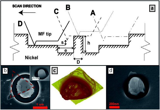 | ||
| Fig. 14 (a) 2D sketch of scanning by MF tip of a pillar carved at the center of a trench. The contact is on one side in phase A, the scanning tooth images the pillar in phase B, the flat surface touches the pillar top in phase C and the scanning tooth is again in contact with the surface in phase D. Clearance quotes “s” and “e” in the sketch determine the feasibility of the compression test in relation to the amount of offset of the scanning tooth and the extent of the flat portion of the tip. Compression or shear test is done in position C. (b and c) SEM and AFM images of a 700 nm pillar after eccentric compression by MF tip that sheared the column. In the SEM top view, the trace of the indenter tip is shown (dashed line). (d) Damage caused on the pillar by the MF tip during scanning at excessive velocity. The staircase profile “machined” by the MF tip on the right side of the pillar top is evident. | ||
The MF tip experience demonstrated also another side of nanomechanics, more relevant to manufacturing than testing. The ability to perform controlled shear tests implies in fact that the very same methodology can be deployed for metal-forming processes of MEMS and NEMS components, using purposely engineered special tips to shape basic nanosamples via work hardening, forging, etc., just like at the macroscale. The opportunity to develop formability-based micro-fabrication had been invoked long before to overcome, for example, complication of conventional lithography.44,45
Even metal cutting can be envisioned to be performed in the same setting, since the MF tip can be set in relative motion (as in ordinary SPM) at sustained speed. The sample damage, shown in Fig. 14(d) and caused by the MF tip hitting a small nanopost with a relatively high impact velocity, provides a visual confirmation as far as metal cutting potential.
Conclusions
Nanomechanics is a reign of sample-size dependent effects, both in plasticity and fracture, which makes the mechanical characterization of materials necessary to MEMS design, as manufacturing techniques improve and MEMS components shrink in size. The effects surveyed here are representative of the state of the art in a field that is evolving almost in real-time. None of them is yet accounted for, neither in commercial finite element codes endowed with MEMS nor in technical standards (let alone ISO 14577 and ASTM E2546). On top of that, controlling extrinsic effects is a significant challenge in nanoscale testing and MEMS design, almost as important as the characterization of intrinsic properties itself. The discussion supports that MEMS and NEMS are at the crossroad of materials science and structural analysis and design, which both need to work synergically towards sound metrological foundations and new size-dependent design principles suitable for MEMS. Developing standards is currently possible and highly timely in a few areas, such as pillars testing for plasticity.Major issues to be investigated in nanomechanics in the near future are too many to be named in all, but certainly include “the size and internal structure leading to the strongest materials, i.e. the structure–property relations”, “the role of environmental stimuli (thermal conditions, electric field, magnetic field, corrosion, etc.) towards size-dependent plasticity and fracture”, “the role of these enhanced plastic properties on fatigue and creep life”, etc., just to mention a few.
Acknowledgements
The authors gratefully acknowledge Prof. Vincent Aimez, Prof. Paul G. Charette, and Dr Julie Verstraeten, at the Département de génie électrique et de génie informatique, Centre de Recherche en Nanofabrication et en Nanocaractérisation (CRN2), Université de Sherbrooke, Qc, Canada for their support, in particular for kindly providing the images of their 3D force transducer MEMS. The access to the LeRoy Eyring Center for Solid State Science and the support by Prof. Karl Sieradzki and Prof. Pedro Peralta at Arizona State University are gratefully acknowledged.Notes and references
- M. D. Uchic, D. M. Dimiduk, J. N. Florando and W. D. Nix, Science, 2004, 305, 986–989 CrossRef CAS.
- A. Rinaldi, P. Peralta, C. Friesen and K. Sieradzki, Acta Mater., 2008, 56, 511–517 CrossRef CAS.
- M. D. Uchic, P. A. Shade and D. M. Dimiduk, Annu. Rev. Mater. Res., 2009, 39, 361–386 CrossRef CAS.
- A. Rinaldi, Damage Mechanics and Micromechanics of Localized Fracture Phenomena in Inelastic Solids, CISM Course Series, ed. G. Voyiadjis, Springer, 2011, Vol. 525, ISBN 978-3-7091-0426-2 Search PubMed.
- W. M. Mook, J. D. Nowak, C. R. Perrey, C. B. Carter, R. Mukherjee, S. L. Girshick, P. H. McMurry and W. W. Gerberich, Phys. Rev. B: Condens. Matter Mater. Phys., 2007, 75, 214112 CrossRef.
- A. Rinaldi, P. Peralta, C. Friesen, N. Chawla, E. Traversa and K. Sieradzki, J. Mater. Res., 2009, 24(No. 3), 768–775 CrossRef CAS.
- A. Rinaldi, P. Peralta, C. Friesen, D. Nahar, S. Licoccia, E. Traversa and K. Sieradzki, Small, 2010, 6(4), 528–536 CrossRef CAS.
- Atomistic simulations of nanomechanics of nanostructures, MRS Bull., ed. H. Huang and H. Van Swygenhoven, 2009, Vol. 34, p. 3. Search PubMed.
- K. Sieradzki, A. Rinaldi, C. Friesen and P. Peralta, Acta Mater., 2006, 54, 4533 CrossRef CAS.
- It would be pretentious and perhaps erroneous to state that FCC materials were investigated first due to their single slip deformation because other factors were surely influential to this choice, such as the ability to manufacture these materials (e.g.Cu, Au, Ag, Ni, NiFe, ferrous cobalt alloys, etc.) at thicknesses accessible to the MEMS and nanotechnology industry using inexpensive electroforming techniques.
- S. S. Brenner, J. Appl. Phys., 1956, 27, 1484–1491 CrossRef CAS.
- J.-Y. Kim, D. Jang and J. R. Greer, Acta Mater., 2010, 58(7), 2355–2363 CrossRef CAS.
- J. R. Greer and W. D. Nix, Phys. Rev. B: Condens. Matter Mater. Phys., 2006, 73, 061624.
- W. Shan, R. K. Mishra, S. A. S. Asif, O. Warren and A. M. Minor, Nat. Mater., 2007, 7, 115–119.
- A. Rinaldi, M. A. Correa-Duarte, V. Salgueirino-Maceira, S. Licoccia, E. Traversa, A. B. Dávila-Ibáñez, P. Peralta and K. Sieradzki, Acta Mater., 2010, 58(19), 6474–6486 CrossRef CAS.
- A. Rinaldi, S. Licoccia, E. Traversa, K. Sieradzki, P. Peralta, A. B. Dávila-Ibáñez, M. A. Correa-Duarte and V. Salgueirino, J. Phys. Chem. C, 2010, 114(32), 13451–13458 CAS.
- W. W. Gerberich, W. M. Mook, C. R. Perrey, C. B. Carter, M. I. Baskes, R. Mukherjee, A. Gidwani, J. Heberlein, P. H. McMurry and S. L. Girshick, J. Mech. Phys. Solids, 2003, 51, 979–992 CrossRef CAS.
- W. W. Gerberich, W. M. Mook, M. J. Cordill, C. B. Carter, C. R. Perrey, J. V. Heberlein and S. L. Girshick, Int. J. Plast., 2005, 21, 2391–2405 CrossRef CAS.
- M. Zou and D. Yang, Tribol. Lett., 2006, 22(2), 189–196 CrossRef CAS.
- P. Valentini, W. W. Gerberich and T. Dumitrică, Phys. Rev. Lett., 2007, 99, 175701 CrossRef CAS.
- J. Ye, R. K. Mishra, A. R. Pelton and A. M. Minor, Acta Mater., 2010, 58(2), 490–498 CrossRef CAS.
- About the two parameters of the Weibull distribution, the former parameter m characterizes the spread of the strength distribution (2) and reflects to the density of defects of the material volume, i.e. the degree of heterogeneity. It tends to infinity for very ordered systems, when the distribution resembles a spike.
- H. Bei, S. Shim, G. M. Pharr and E. P. George, Effects of prestrain on the compressive stress–strain response of Mo-alloy single-crystal micropillars, Acta Mater., 2008, 56, 4762–4770 CrossRef CAS.
- Eqn (8) follows from the same derivation used for eqn (7) by replacing eqn (3) with F(σ;S) = F(σREF;SREF).
- The high P-value from the Anderson–Darling goodness of fit test indicates that the fit is acceptable. This is a perfectly legitimate procedure if the defects density remains constant for the considered volume range, which is the underlying assumption of this theory. Only then, m is a sample independent intrinsic property of a nanomaterial, i.e. measurable from a set of pillars (or other samples) with arbitrarily chosen dimension. Despite the good results shown here, this hypothesis requires a thorough validation, bearing in mind that both estimates of m (the indirect one from the power law exponents in eqn (7) and (8) and the direct one from the fitted distributions eqn (2) from experimental histograms) should be obtained from many samples over an D range as large as possible for statistical significance sake. In this respect it should be recalled that as a rule of thumb a minimum of 50 to 100 observations is necessary to accurately identify the shape of sampling distribution.
- M. J. Burek and J. R. Greer, Nano Lett., 2009, 10, 69–76.
- R. Maaβ, D. Grolimund, S. V. Petegem, M. Willimann, M. Jensen, H. V. Swygenhoven, T. Lehnert, M. A. M. Gijs, C. A. Volkert, E. T. Lilleodden and R. Schwaiger, Appl. Phys. Lett., 2006, 89(15), 151905 CrossRef.
- It is indicative that anisotropic theory is not a standard part of mechanical engineering education despite the widespread use of composite materials in the industry. The gap with the isotropic theory is also reflected, for example, by the current theory of contact mechanics, which is used in nanomechanics (e.g. Oliver–Pharr test or the Sneddon correction) despite being based on isotropic elasticity.
- W. W. Gerberich, W. M. Mook, M. J. Cordill, J. M. Jungk, B. Boyce, T. Friedmann, N. R. Moody and D. Yang, Int. J. Fract., 2006, 138, 75–100 CrossRef CAS.
- D. Kiener, W. Grosinger, G. Dehm and R. Pippan, Acta Mater., 2008, 56, 580–592 CrossRef CAS.
- D. S. Gianola, G. Richter, A. Sedlmayr, R. Moenig, B. Roos, C. A. Volkert and O. Kraft, MRS fall 2009, proceedings.
- F. Östlund, K. Rzepiejewska-Malyska, K. Leifer, L. M. Hale, Y. Tang, R. Ballarini, W. W. Gerberich and J. Michler, Adv. Funct. Mater., 2009, 19(15), 2439–2444 CrossRef.
- R. Li and K. Sieradzki, Ductile-brittle transition in random porous Au, Phys. Rev. Lett., 1992, 68, 1168–1171 CrossRef CAS.
- C. L. Muhlstein, E. A. Stach and R. O. Ritchie, Acta Mater., 2002, 50(14), 3579–3595 CrossRef CAS.
- H. Kahn, L. Chen, R. Ballarini and A. H. Heuer, Acta Mater., 2006, 54, 667–678 CrossRef CAS.
- J. Bagdahn and W. N. Sharpe, Jr, Sens. Actuators, A, 2003, 103, 9 CrossRef.
- J. D. Williams, International Journal of Theoretical and Applied Multiscale Mechanics, 2010, 1(3), 266–279 Search PubMed.
- W. C. Oliver and G. M. Pharr, J. Mater. Res., 1992, 7, 1564 CrossRef CAS.
- Note the largest slip extent of order of 0.5% strain, translating into a modest plastic displacement of less than 1 nm in these buttons as h ≈ 110–120 nm.
- D. Kiener, C. Motz and G. Dehm, J Mater. Sci., 2008, 43, 2503–2506 CrossRef CAS.
- D. Kiener, C. Motz and G. Dehm, Mater. Sci. Eng., A, 2009, 505, 79–87 CrossRef.
- D. Kiener, W. Grosinger and G. Dehm, Scr. Mater., 2009, 60, 148–151 CrossRef CAS.
- In essence, Saint-Venant's principle states that the (localized) strains and stresses produced in the body by a system of statically equilibrated forces (i.e. resulting in zero force and zero couple) applied to a small part of its surface are of negligible magnitude at distances large compared with the linear dimensions of the loaded zone (represented by D here).
- X. Li, H. Gao, X. J. Murphy and K. K. Caswell, Nano Lett., 2003, 3(11), 1495–1498 CrossRef CAS.
- F. F. Csikor, C. Motz, D. Weygand, M. Zaiser and S. Zapperi, Science, 2007, 318, 251–254 CrossRef CAS.
Footnote |
| † Electronic supplementary information (ESI) available: Extreme Value Theory principles. See DOI: 10.1039/c0nr00699h |
| This journal is © The Royal Society of Chemistry 2011 |