Guided assembly of metal and hybrid conductive probes using floating potential dielectrophoresis†
Josep
Puigmartí-Luis
*a,
Johannes
Stadler
a,
Daniel
Schaffhauser
a,
Ángel Pérez
del Pino
b,
Brian R.
Burg
c and
Petra S.
Dittrich
*a
aDepartment of Chemistry and Applied Biosciences, ETH Zürich, 8093, Zürich, Switzerland. E-mail: puigmarti.luis@org.chem.ethz.ch; dittrich@org.chem.ethz.ch; Tel: +41-44-6336893
bInstitut de Ciéncia de Materials de Barcelona (CSIC), Campus Universitari, 08193, Bellaterra, Spain
cDepartment of Mechanical and Process Engineering, ETH Zürich, 8092, Zürich, Switzerland
First published on 11th January 2011
Abstract
We present the site-selective, parallel and reproducible formation of conductive gold and tetrathiafulvalene–gold (TTF–Au) hybrid micro- and nanowires from their respective ion salt and cation-radical solutions. While the formation of micro- and nanowires by means of dielectrophoresis with directly coupled electrodes has been thoroughly investigated in recent studies, we present here the first relevant example of metal and hybrid wire assembly obtained by floating potential dielectrophoresis. In this configuration, the assembly of micro- and nanowires is achieved by capacitively coupling a large electrode (bias electrode) to a conductive substrate (p-doped Si) separated by an insulating oxide layer. In contrast to former studies, this allows parallel production of micro- and nanowires with only one pair of electrodes connected to a sine wave generator. We further demonstrate that these structures are suitable probes for localized surface enhanced Raman spectroscopy (SERS).
One-dimensional materials such as nanowires, nanorods and nanotubes are of central interest for the construction of nanoscale devices. While much effort was invested in the past to improve bottom-up formation processes of metal or soft matter nanostructures, alternative materials such as hybrid systems created from metal salts and organic compounds have gained considerable interest. Due to their tunable properties,1 these materials are particularly valuable for the construction of novel multifunctional nanoscale devices.2 In particular, hybrid materials based on tetrathiafulvalene (TTF) and its derivatives have been well investigated in recent years,3 and TTF salts have been prepared with various electrical, magnetic and optical characteristics. It is well known that TTF derivatives can produce low-dimensional organic charge-transfer salts by electrocrystallization from solution.4 However, although there are a few strategies for the electrochemical nucleation and growth of charge-transfer salts based on TTF derivatives,5 the electrochemical formation and deterministic positioning of TTF hybrid systems remain a significant challenge. Previous studies have demonstrated that conductive functional hybrid materials made of TTF–Au can be formed either by chemical reaction using bulk synthesis methods6 or by using a microfluidics based technology.7 However, these approaches do not lead to local growth or positioning of the structures.
In the past, significant advances have been achieved in developing new methods for the controlled bottom-up formation and deterministic positioning of micro- and nanowires. These approaches include seed template processes,8 microfluidics9 and dielectrophoretic (DEP) assembly from solution. In the latter case, the majority of the work reported is based on the assembly of metallic nanoparticles from solution between directly coupled electrodes.10 More recently, the same methodology was employed for the formation of metallic (micro-)wires from aqueous salt solutions.11–15 A related method is floating potential dielectrophoresis employing capacitively coupled electrodes. This dielectrophoretic technique has long been used to selectively achieve alignment, as well as to trap individual structures at multiple predefined locations with a single electrical connection.16–20
The unique combination of controlled growth of micro- and nanowires from solution and the employment of floating potential DEP has, however, not been demonstrated to date.
In this paper we report a method for the site specific growth of gold and tetrathiafulvalene–gold (TTF–Au) hybrid micro- and nanowires. These structures are assembled from their respective ion salt and cation-radical solutions by applying alternating electric fields in a capacitively coupled configuration. In contrast to assemblies formed by DEP with directly coupled electrodes, in our approach resistive heating through the assembled structures is avoided and hence, any damage during the formation process is prevented. This approach is remarkably advantageous because of its potential to massively parallelize the formation process. In floating-potential dielectrophoresis, only two connections to external devices are required, regardless of the number of counter electrodes (CEs) placed on the microchip, and hence, the chip dimensions can be considerably reduced. The formed structures are readily attached to the electrodes for further characterisation and application without the need of complicated and time consuming post-processing methods. Additionally, we illustrate that these structures are suitable probes for localized surface enhanced Raman spectroscopy (SERS).
In the experiments we used microchips with an electrode configuration as shown in Fig. 1. The entire chip contained 20 electrode pairs of individual counter electrodes (CEs) and a large bias electrode (BE). The parallel assembly of wires between the electrode pairs was achieved by capacitively coupling the bias electrode to a conductive substrate (p-doped Si) separated by an insulating silicon oxide layer (Fig. 1(b)).21 In a typical experiment, a drop (ca. 5 µL) of either hydrogen tetrachloroaurate (0.2 mM) or TTF–Au precursor solution, both in acetonitrile covered the entire chip (see ESI† for the detailed solution characterisation). A sine wave of 5 Vp at a frequency of 1 MHz was applied between the BE and the doped silicon substrate until the solvent was evaporated. The CE, which is 2 µm apart from the bias electrode tip remained on a floating potential. This configuration used with the noted experimental conditions enables the formation of vortices above the tapered electrode tips in the areas of highest electrical field strength.20 Therefore, the dielectrophoretic forces cause the ionic species to drift toward the region of highest electrical field strength,12,14,15 which is at the tip of the electrode and subsequently of the wire. At this location, electrochemical deposition and the site-specific growth of both bare gold and TTF–Au wires were possible as demonstrated by scanning electron microscopy (SEM) images (Fig. 1(c) and (e)). The assembly of the micro- and nanostructures between the electrode gaps lasted for less than 60 seconds. The structure widths achieved in this case ranged typically between 50 nm and 500 nm as determined by SEM and atomic force microscopy (AFM).
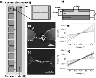 | ||
| Fig. 1 (a) Schematic representation of 10 counter electrodes (CEs) with a common bias electrode (BE) used in the experiments (top view). (b) Schematic diagram of the capacitively coupling employed during the DEP studies (side view). SEM images of assembled (c) bare gold and (e) TTF–Au nanowires bridging electrode pairs and curves showing I–V characteristics for different electrode pairs of (d) bare gold and (f) TTF–Au wires, respectively. The I–V characterisation was performed for every electrode pair with a probe station under ambient conditions. The plots in (d) and (f) correspond each to a single chip containing 20 individual electrode pairs. The number of conductive wires in (d) is 10 and (f) is 18. | ||
Frequently, we found the formation of branched micro- and nanowires (Fig. S1 and S2†). This was observed in former studies on DEP-based formation of metal wires as well.11,12
In order to better understand the mechanism underlying the hybrid wire formation from solution, we compare it with the growth of bare gold wires from its ion salt solution. When alternating electric fields are applied, it is assumed that the gold ions reduce viaelectron transfer at the electrode tips, where the electric field gradient is highest.12,14,15,22 Therefore, electrochemical metal deposition and wire formation occur. In the case of TTF–Au wire growth, it has been shown that charge transfer between gold and TTF molecules is favourable.23 Therefore, absorption of TTF molecules viaelectron transfer can be possible, along with the electrochemical deposition of gold ions present in the TTF–Au solution. With reference to the cyclic voltammograms (Fig. S3†), we assume that the negative potential applied to the BE is large enough for the gold ion species and TTF molecules to spontaneously react towards the TTF–Au hybrid composites. Additional SERS and energy-dispersive X-ray spectroscopy (EDX) experiments indicate that this is in fact the case (see ESI† for EDX characterisation and additional SERS measurements).
Additionally, I–V properties of the microjunctions were measured as a function of the bias voltage applied between the two electrodes. Usually, between 50 and 90% of the electrode pairs were bridged by a conductive wire. In general, we obtained a higher yield of formation of conductive TTF–Au wires compared to bare gold wires. This preferential formation of TTF–Au wires can be attributed to the increase of ionic pairs in the initial solution, as previously reported in related work.14,15 For all the wires, we measured similar I–V characteristics and the direct current analysis revealed no significant differences between bare gold and TTF–Au wires (Fig. 1(d) and (f)). In all cases the wires showed ohmic behavior with resistances on the order of 1 kΩ. The fact that all values lie within the same order of magnitude demonstrates the robustness of the parallel integration method. When voltages exceeded 1 V, the contact of the wires with the electrodes broke down, which was also confirmed by SEM analysis (Fig. S4†).
To test the current flow through the branched structures, we carried out current-sensing atomic force microscopy (CS AFM) studies using the setup illustrated in Fig. 2(a) (see ESI† for further details). In these studies, a bias voltage to the BE electrode was applied while scanning with a grounded conductive tip. Fig. 2(b) and (c) show resistance maps of hybrid TTF–Au microjunctions measured with CS AFM. Clearly, this result indicates that the resistivity of the branches is of the same order as the resistivity measured for the wire (Fig. 2(b)).24 As can be seen in Fig. 2(c), when a pair of electrodes is not bridged, the CE remains grounded, and hence, it does not appear in the resistance map. Fig. 3 demonstrates that this is in fact the case.
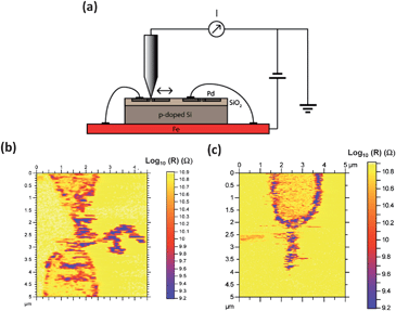 | ||
| Fig. 2 (a) Schematic representation of the set-up used for the CS AFM measurements. (b) and (c) are resistance maps of hybrid TTF–Au microjunctions grown between electrode pairs. | ||
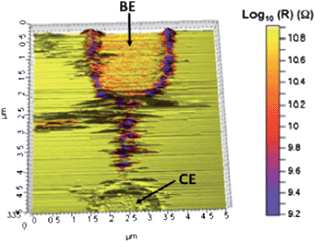 | ||
| Fig. 3 3D topography AFM image and the corresponding resistance map of a TTF–Au wire. Arrows mark the bias electrode (BE) and the counter electrode (CE). | ||
Furthermore, we employed Raman spectroscopy to characterize the wires. In contrast to standard SERS experiments, where a rough noble metal surface or small particles made of silver or gold are used to enhance signals,25 we can address the exact location and restrict the enhancement of signals to the wires confined between the electrode pairs. In Fig. 4(a) and (b) 3D atomic force microscopy (AFM) images from a hybrid branched and bare gold wire, respectively, are shown color coded with the optical response of the addressed structures, as determined by confocal Raman spectroscopy. The evaluation of the Raman map at the intensity of the 501 cm−1 band, a typical marker band of TTF+˙, clearly proves that TTF signals are emitted from the hybrid structures located between the electrode pairs. The bare gold wires shown in Fig. 4(b) also enhance signals as indicated by the brighter areas between the electrodes. A careful examination of the attributed spectra reveals, however, that the increase in signal levels in the TTF marker band region is due to the enhanced background noise and not due to a specific Raman signal from within the structure. The spectra do not show any signature bands from TTF molecules, and only emit signals from enhanced carbonaceous contaminations (Fig. S6†). We further compared the full Raman spectra from the stock solution that was used to grow the micro- and nanowires and that of the TTF–Au wire on the silicon oxide surface (Fig. 4(c) and (d), respectively). The SERS spectra from the TTF–Au solution clearly show typical Raman bands of TTF+˙ at 501 cm−1, 748 cm−1, 1418 cm−1 and 1514 cm−1. These bands correspond well with the literature values of TTF on gold with peaks located at 506 cm−1, 748 cm−1 and 1418 cm−1.26 The band at 1514 cm−1 indicates that small amounts of TTF0 are present in the solution. In Fig. 4(d), representative Raman spectra from a TTF–Au wire as well as a background spectrum from the chip are shown. Due to short integration times, the noise level of the spectra from the wires is higher than that of the background and the TTF–Au solution SERS spectra. However, five typical TTF+˙ bands at 500 cm−1, 1288 cm−1, 1423 cm−1 and 1448 cm−1 as well as 1514 cm−1 could be found in the area containing the hybrid structures, unambiguously proving the presence of TTF in these wires. With a background level of 30 counts from the red curve and a signal of 900 counts in the main band of the grey curves, an enhancement by at least a factor of 30 can be attributed to the addressable structures.
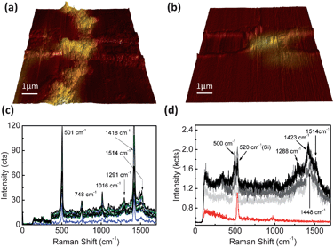 | ||
| Fig. 4 (a) and (b) 3D AFM topography images from two wires between electrodes of TTF–Au and bare gold, respectively. The color represents the intensity of the Raman TTF marker bands at equal locations. (c) Surface enhanced Raman spectra of TTF–Au stock solution at different positions on a 6 nm rough silver cover slip. (d) Confocal Raman spectra from enhanced TTF molecules in hybrid wire areas (grey tones) and the background spectra (red). | ||
In summary, hybrid TTF–Au and bare gold wires have been successfully synthesized and patterned from TTF cation-radical and gold ion salt solutions by using floating potential DEP. For the first time, localized hybrid micro- and nanowire formation from cation-radical salt solution was demonstrated, in contrast to previous studies where just pure metal wires had been synthesized. Floating potential DEP enables large parallelization and integration during the assembly process thereby showing high performance and high reproducibility. With such an approach, the wires are rapidly assembled and can be used immediately after its fabrication without the need for any postfabrication processes. Furthermore, the results demonstrate the guided and site-selective synthesis of surface-enhanced Raman probes. The capability to prepare functional assemblies and ultimately useful systems with their growth at a desirable location is particularly important for the in situ integration of electronic circuits, and for the development of new surface plasmonic sensors. Further research will focus on the preparation of new hybrid materials integrated with microfluidic systems and their application as sensing devices with both optical and electrical readouts.
Acknowledgements
The authors acknowledge the Electron Microscopy Center of the ETH Zurich (EMEZ) for their facilities, funding from the European Research Council under the 7th Framework Programme (ERC Starting Grant, project no. 203428, “nm-LIPIDS”), and the ETH for fellowship to J.P.-L. The authors also thank Sieglinde Ebner for EPR measurements, Christoph Mayer for XPS analysis and Rob Nieckarz for useful discussion.Notes and references
- J. van Herrikhuyzen, S. J. George, M. R. J. Vos, N. A. J. M. Sommerdijk, A. Ajayaghosh, S. C. J. Meskers and A. P. H. J. Schenning, Angew. Chem., Int. Ed., 2007, 46, 1825 CrossRef CAS; J. Puigmartí-Luis, Á. Pérez del Pino, E. Laukhina, J. Esquena, V. Laukhin, C. Rovira, J. Vidal-Gancedo, A. G. Kanaras, R. J. Nichols, M. Brust and D. B. Amabilino, Angew. Chem., Int. Ed., 2008, 47, 1861 CrossRef.
- C. Joachim, J. K. Gimzewski and A. Aviram, Nature, 2000, 408, 541 CrossRef CAS; W. U. Huynh, J. J. Dittmer and A. P. Alivisatos, Science, 2002, 295, 2425 CrossRef CAS.
- E. Coronado, J. R. Galán-Mascarós, C. J. Goméz-García and V. Laukhin, Nature, 2000, 408, 447 CrossRef CAS; E. Coronado and P. Day, Chem. Rev., 2004, 104, 5419 CrossRef; E. Coronado, C. Giménez-Saiz, C. J. Gómez-García and S. C. Capelli, Angew. Chem., Int. Ed., 2004, 43, 3022 CrossRef CAS; B. Zhang, Z. Wang, H. Fujiwara, H. Kobayashy, M. Kurmoo, K. Inoue, T. Mori, S. Gao, Y. Zhang and D. Zhu, Adv. Mater., 2005, 17, 1988 CrossRef; S. A. Baudron, P. Batail, C. Coulon, R. Clérac, E. Canadell, V. Laukhin, R. Melzi, P. Wzietek, D. Jérome, P. Auban-Senzier and S. Ravy, J. Am. Chem. Soc., 2005, 127, 11785 CrossRef CAS; R. J. Brea, L. Castedo, J. R. Granja, M. A. Herranz, L. Sánchez, N. Martín, W. Seitz and D. M. Guldi, Proc. Natl. Acad. Sci. U. S. A., 2007, 104, 5291 CrossRef CAS.
- A. C. Hillier and M. D. Ward, Science, 1994, 263, 1261 CAS.
- P. Batail, K. Boubekeur, M. Fourmigué and J.-Ch.P. Gabriel, Chem. Mater., 1998, 10, 3005 CrossRef CAS; A. Deluzet, S. Perruchas, H. Bengel, P. Batail, S. Molas and J. Fraxedas, Adv. Funct. Mater., 2002, 12, 123 CrossRef CAS; T. G. Prokhorova, S. S. Khasanov, L. V. Zorina, L. I. Buravov, V. A. Tkacheva, A. A. Baskakov, R. B. Morgunov, M. Gener, E. Canadell, R. R. Shibaeva and E. B. Yagubskii, Adv. Funct. Mater., 2003, 13, 403 CrossRef CAS; M. Mas-Torrent and P. Hadley, Small, 2005, 1, 806 CrossRef CAS.
- K. Naka, D. Ando, X. Wang and Y. Chujo, Langmuir, 2007, 23, 3450 CrossRef CAS.
- J. Puigmartí-Luis, D. Schaffhauser, B. R. Burg and P. S. Dittrich, Adv. Mater., 2010, 22, 2255 CrossRef CAS.
- M. Huang, S. Mao, H. Feick, H. Q. Yan, Y. Y. Wu, H. Kind, E. Weber, R. Russo and P. D. Yang, Science, 2001, 292, 1897 CrossRef CAS; P. A. Gao, Y. Ding and Z. L. Wang, Nano Lett., 2003, 3, 1315 CrossRef CAS.
- P. J. A. Kenis, R. F. Ismagilov and G. M. Whitesides, Science, 1999, 285, 83 CrossRef CAS; B. Messer, J. H. Song and P. Yang, J. Am. Chem. Soc., 2000, 122, 10232 CrossRef CAS.
- K. D. Hermanson, S. O. Lumsdon, J. P. Williams, E. W. Kaler and O. D. Velev, Science, 2001, 294, 1082 CrossRef; S. O. Lumsdon and D. M. Scott, Langmuir, 2005, 21, 4874 CrossRef CAS; B. C. Gierhart, D. G. Howitt, S. J. Chen, R. L. Smith and S. D. Collins, Langmuir, 2007, 23, 12450 CrossRef CAS; R. J. Barsotti, Jr, M. D. Vahey, R. Wartena, Y. M. Chiang, J. Voldman and F. Stellacci, Small, 2007, 3, 488 CrossRef; S. H. Yoon, S. Kumar, G. H. Kim, Y. S. Choi, T. W. Kim and S. I. Khondaker, J. Nanosci. Nanotechnol., 2008, 8, 3427 CrossRef CAS.
- Ch. Cheng, R. K. Gonela, Q. Gu and D. T. Haynie, Nano Lett., 2005, 5, 175 CrossRef CAS.
- N. Ranjan, H. Vinzelberg and M. Mertig, Small, 2006, 2, 1490 CrossRef CAS.
- I. Talukdar, B. Ozturk, T. D. Mishima and B. N. Flanders, Appl. Phys. Lett., 2006, 88, 221907 CrossRef.
- B. Ozturk, I. Talukdar and B. N. Flanders, Nanotechnology, 2007, 18, 365302 CrossRef.
- N. Ranjan, M. Mertig, G. Cuniberti and W. Pompe, Langmuir, 2010, 26, 552 CrossRef CAS.
- P. A. Smith, C. D. Nordquist, T. N. Jackson, T. S. Mayer, B. R. Martin, J. Mbindyo and T. E. Mallouk, Appl. Phys. Lett., 2000, 77, 1399 CrossRef CAS.
- L. Dong, V. Chirayos, J. Bush, J. Jiao, V. M. Dubin, R. V. Chebian, Y. Ono, J. F. Conley, Jr and B. D. Ulrich, J. Phys. Chem. B, 2005, 109, 13148 CrossRef CAS.
- R. Krupke, F. Hennrich, H. B. Weber, M. M. Kappes and H. V. Löhneysen, Nano Lett., 2003, 3, 1019 CrossRef CAS.
- S. Golan, D. Elata, M. Orenstein and U. Dinnar, Electrophoresis, 2006, 27, 4919 CrossRef CAS.
- B. R. Burg, V. Bianco, J. Schneider and D. Poulikakos, J. Appl. Phys., 2010, 107, 124308 CrossRef.
- B. R. Burg, J. Schneider, M. Muoth, L. Durrer, T. Helbling, N. C. Schirmer, T. Schwamb, C. Hierold and D. Poulikakos, Langmuir, 2009, 25, 7778 CrossRef CAS.
- B. Ozturk, B. N. Flanders, D. R. Grischkowsky and T. D. Mishima, Nanotechnology, 2007, 18, 175707 CrossRef.
- V. T. Joy and T. K. K. Srinivasan, Chem. Phys. Lett., 2000, 328, 221 CrossRef CAS.
- Note that the probe-microjunction contact area lies in the nanometre scale, leading to the formation of an additional nanocontact resistance (also called spreading resistance) which usually is several orders of magnitude higher than the conventional contact resistance measured on the macroscale.
- R. G. Freeman, K. C. Grabar, K. J. Allison, R. M. Bright, J. A. Davis, A. P. Guthrie, M. B. Hommer, M. A. Jackson, P. C. Smith, D. G. Walter and M. J. Natan, Science, 1995, 267, 1629 CrossRef CAS; Ch. E. Talley, J. B. Jackson, C. Oubre, N. K. Grady, C. W. Hollars, S. M. Lane, T. R. Huser, P. Nordlander and N. J. Halas, Nano Lett., 2005, 5, 1569 CrossRef CAS.
- C. J. Sandroff, D. A. Weltz, J. C. Chung and D. R. Herschbach, J. Phys. Chem., 1983, 87, 2127 CrossRef CAS.
Footnote |
| † Electronic supplementary information (ESI) available: Additional SEM, EDX, XPS, SERS measurements and detailed experimental section are provided. See DOI: 10.1039/c0nr00681e |
| This journal is © The Royal Society of Chemistry 2011 |