Double-walled carbon nanotubes: Challenges and opportunities
Cai
Shen
,
Alexandra H.
Brozena
and
YuHuang
Wang
*
Department of Chemistry and Biochemistry, University of Maryland, College Park, MD 20742, USA. E-mail: yhw@umd.edu
First published on 1st November 2010
Abstract
Double-walled carbon nanotubes are coaxial nanostructures composed of exactly two single-walled carbon nanotubes, one nested in another. This unique structure offers advantages and opportunities for extending our knowledge and application of the carbon nanomaterials family. This review seeks to comprehensively discuss the synthesis, purification and characterization methods of this novel class of carbon nanomaterials. An emphasis is placed on the double wall physics that contributes to these structures’ complex inter-wall coupling of electronic and optical properties. The debate over the inner-tube photoluminescence provides an interesting illustration of the rich photophysics and challenges associated with the myriad combinations of the inner and outerwall chiralities. Outerwall selective covalent chemistry will be discussed as a potential solution to the unattractive tradeoff between solubility and functionality that has limited some applications of single-walled carbon nanotubes. Finally, we will review the many different uses of double-walled carbon nanotubes and provide an overview of several promising research directions in this new and emerging field.
 Cai Shen | Cai Shen received his PhD degree under the supervision of Dr Manfred Buck from the University of St Andrews, UK, in 2008 and subsequently, worked as a postdoctoral research fellow in the same group. In 2010 he joined Prof. Wang's group as a postdoctoral research associate. His research interests include surface chemistry, self-assembled monolayers, and double-walled carbon nanotubes. |
 Alexandra H. Brozena | Alexandra Brozena completed her B.A. in Environmental Science and English at Tulane University, New Orleans in 2008. She is currently in the third year of the chemistry PhD program at the University of Maryland, College Park in Prof. Wang's group. Her research interests include surface chemistry and chemical separations of carbon nanotubes. |
 YuHuang Wang | YuHuang Wang received his PhD from Rice University with Richard E. Smalley in 2005. After postdoctoral work with Chad A. Mirkin at Northwestern University, he joined the faculty of the University of Maryland in 2008. Professor Wang's research lies at the interface of materials, chemistry, and physics. He is the author of over 40 manuscripts in peer-reviewed journals and 12 patents and applications. |
1. Introduction
Double-walled carbon nanotubes (DWNTs) are an emerging class of carbon nanostructures. A DWNT consists of exactly two concentric carbon nanotubes. This double-wall structure makes DWNTs the simplest system for studying the effects of inter-wall coupling on the physical properties of carbon nanotubes (CNTs). Compared to single-walled carbon nanotubes (SWNTs), DWNTs have higher mechanical strength and thermal stability and they also possess interesting electronic and optical properties. Although DWNTs were discovered in 1991 and the first synthesis was reported in 1998, this structure has received relatively little attention until the recent synthesis1 and separation2 of high purity samples. In this article, we will review the recent development of DWNTs and compare DWNTs with other carbon nanostructures with the goal of providing a reasonable trajectory of future research directions for this interesting nanostructure.We will start with a brief historic overview, after which the structure of DWNTs will be elucidated and classified. We will focus on several key questions: (1) How are DWNTs synthesized? What controls the growth of DWNTs? Why do DWNTs grow preferentially over SWNTs? (2) What makes DWNTs unique with respect to structure, physical properties and chemistry? Is there any potential application of which DWNTs are advantageous compared to other carbon nanostructures such as SWNTs and multi-walled carbon nanotubes (MWNTs)? A major component of this article will be devoted to outerwall selective chemistry. In particular, we will introduce outerwall selective chemistries developed in our group that produce water soluble DWNTs while simultaneously retaining the electrical conductivity of the inner-tube. We propose that outerwall selective functionalization will be the key next step to studying fundamental properties of DWNTs, to take maximum advantage of this unique double-wall structure, and to achieve many potential applications of carbon nanotubes. The review will be concluded with a brief account of key challenges confronting DWNT research and promising future research directions.
2. Synthesis and purification
DWNTs can be synthesized by arc-discharge, catalytic chemical vapor deposition (CCVD), and “peapod” methods. These methods are not vastly different from those used to prepare SWNTs. However, subtle changes of temperature, pressure, carbon feedstock, and catalytic composition can lead to the preferential growth of DWNTs rather than SWNTs and MWNTs. Table 1 summarizes the synthetic methods for DWNTs as well as SWNTs and MWNTs. It is interesting to note that the thermal and mechanical properties of CNTs depend heavily on how they are synthesized (arc-discharge, CCVD, or peapod). This dependence is probably correlated with the varying quality of the CNTs (defects, diameter, and length) synthesized by these different methods. In the following sections, we will discuss the three types of synthetic methods and compare the parameters controlling DWNT growth (diameter, yield, purity) which are important to elucidating the mechanism of DWNT synthesis.| Carbon Nanotubes | Size | Preparation methods | Thermal properties | Mechanical properties |
|---|---|---|---|---|
| a (E) Experimental observation; (T) Theoretical prediction. | ||||

|
0.4–several nm in diameter | Laser ablation, Arc-discharge, CVD | Stable up to ∼1800 °C in Ar;132 750 °C in air.133 | Young's modulus: ∼1.8 TPa(E + T)136 |
| Thermal conductivity >3500 Wm−1K−1 or ∼600 Wm−1K−1 produced by CVD.134,135 | Tensile strength: ∼1.0 TPa (E)137 | |||

|
Inter-wall distance 0.33–0.42 nm59 | Arc-discharge, CVD, Peapod method | Stable up to ∼2000 °C in Ar,57 800 °C in air.138 | Young's modulus: 0.73–1.33 TPa (E)139 |
| Thermal conductivity ∼600 Wm−1K−1 produced by CVD.135 | Tensile strength: 13–46 GPa (E)139 | |||

|
Inter-wall distance ∼0.34nm | Laser-ablation, Arc-discharge, CVD, Peapod method | Thermal stability varies with diameter and length.141 | Young's modulus:0.27–0.95 TPa (E)141 |
| Thermal conductivity >3000 Wm−1K−1 produced by arc-discharge,140 42–343 Wm−1K−1 produced by CVD.135 | Tensile strength:11–63 GPa (E)141 |
2.1. Arc-discharge
DWNTs were discovered in 1991, along with MWNTs, by Sumio Iijima in the cathode deposit from an experiment attempting to synthesize C60 by the arc-discharge method.3 The purity and yield of CNTs were significantly improved by T. W. Ebbesen and P. M. Ajayan in 1992.4 However, the selective growth of DWNTs by arc-discharge was not reported until 2001 by J. L. Hutchison et al.5 DWNTs with a purity varying from ∼10–20 wt% to ∼50–70 wt% were prepared in an atmosphere of Ar and H2 mixture (1![[thin space (1/6-em)]](https://www.rsc.org/images/entities/char_2009.gif) :1/v:v) at 350 Torr with a graphite anode containing a catalyst prepared from a mixture of Ni, Co, Fe and S. The synthesized DWNTs have an outer-tube diameter in the range of 1.9–5 nm and an inner-tube diameter in the range of 1.1–4.2 nm, as determined by high-resolution transmission electron microscopy. By systematically studying the synthesis parameters, Y. Saito et al. found that the addition of sulfur and the presence of hydrogen are both indispensable for the selective growth of DWNTs.6 Under optimum preparation conditions (FeS:NiS:CoS = 1:1:1, H2 pressure = 300 Torr), 90% of the CNTs are DWNTs. Byeongchul Ha et al. confirmed that FeS plays a key role for the formation of DWNTs in a hydrogen environment. Without the FeS promoter, only SWNTs were obtained.7 H. Huang et al. confirmed the importance of sulfur but found that high quality DWNTs can also be selectively grown in a hydrogen-free atmosphere by using a bowl-like cathode.8 The bowl-like cathode has an enlarged hot reaction zone that provides more carbon clusters for the formation of DWNTs, which may play a similar role to hydrogen. The additions of a halide (KCl) and rare earth metals (Y/La) are also found to enhance the production of DWNTs.9,10 However, the mechanism of these growth promoters is not clear and the arc discharge technique suffers from a number of disadvantages including low yield. Significant improvement in yield will likely require elucidation of the thermodynamics and kinetics as well as an understanding of the growth and the roles of the growth promoters at the atomic level.
:1/v:v) at 350 Torr with a graphite anode containing a catalyst prepared from a mixture of Ni, Co, Fe and S. The synthesized DWNTs have an outer-tube diameter in the range of 1.9–5 nm and an inner-tube diameter in the range of 1.1–4.2 nm, as determined by high-resolution transmission electron microscopy. By systematically studying the synthesis parameters, Y. Saito et al. found that the addition of sulfur and the presence of hydrogen are both indispensable for the selective growth of DWNTs.6 Under optimum preparation conditions (FeS:NiS:CoS = 1:1:1, H2 pressure = 300 Torr), 90% of the CNTs are DWNTs. Byeongchul Ha et al. confirmed that FeS plays a key role for the formation of DWNTs in a hydrogen environment. Without the FeS promoter, only SWNTs were obtained.7 H. Huang et al. confirmed the importance of sulfur but found that high quality DWNTs can also be selectively grown in a hydrogen-free atmosphere by using a bowl-like cathode.8 The bowl-like cathode has an enlarged hot reaction zone that provides more carbon clusters for the formation of DWNTs, which may play a similar role to hydrogen. The additions of a halide (KCl) and rare earth metals (Y/La) are also found to enhance the production of DWNTs.9,10 However, the mechanism of these growth promoters is not clear and the arc discharge technique suffers from a number of disadvantages including low yield. Significant improvement in yield will likely require elucidation of the thermodynamics and kinetics as well as an understanding of the growth and the roles of the growth promoters at the atomic level.
2.2. Peapod
The hollow tubular structure of CNTs allows them to be used as nano test-tubes or templates for the synthesis of new nanostructures. Fullerene filled SWNTs known as “peapods” were first demonstrated in 1998 by Smith et al. during the purification and annealing treatments of SWNTs produced by the laser ablation method.11 Subsequent work revealed that electron irradiation of the C60 molecules trapped inside a SWNT can induce their diffusion and coalescence.12 This is the first example of producing DWNTs from a C60@SWNT peapod morphology. Since this first example, C60, C70, and ferrocene filled SWNTs have all been used as precursors to prepare DWNTs by annealing in vacuum or inert gas atmosphere.13–17 This subject has been reviewed by R. Pfeiffer et al.18 and interested readers are referred to their article.2.3. Catalytic CVD
Catalytic CVD is the most widely used technique for synthesizing DWNTs. It involves the decomposition of gaseous or volatile carbon compounds over metallic nanoparticles, which serve as catalytic as well as nucleation sites for the initial growth of CNTs. The first example of catalytic CVD produced DWNTs is credited to J. H. Hafner et al.19 who found that catalytic decomposition of C2H4 over a 90:9:1 alumina:Fe:Mo catalyst at 850 °C yielded 70% of DWNTs. Since then, a number of recipes for synthesizing DWNTs have been reported. These methods typically involve changing key experimental parameters including (1) catalyst composition and size;20–23 (2) source of feedstocks;24,25 (3) using templates/supporting materials, such as zeolites,26 porous silica27 or MgO,28 and fumed alumina;29 (4) plasma-enhanced CVD;30 (5) water/oxygen assisted CVD.31–33
A small amount of water has been shown to significantly increase the yield of SWNTs.34–36 The water-assisted CVD method allows synthesis of vertically aligned arrays of CNTs with heights up to 2.5 millimeters, providing nanotube material with a carbon purity above 99.98%.36 Extending this method to DWNTs was achieved by precisely controlling the thickness of the Fe catalyst thin film (1.6–1.9 nm for DWNTs instead of 0.8–1.2 nm for SWNTs). T. Yamada et al. reported an 85% DWNT yield when the Fe film thickness was 1.69 nm (Fig. 1).37 By lithographically patterning catalyst islands, arrays of rectangular parallelepipeds with 150 mm width, 250 mm pitch and a height of ∼500 μm can be obtained (Fig. 1g–j). However, the DWNTs obtained by this method have an average diameter of 3.7 nm which can easily collapse.38 Selective growth of small diameter DWNTs in a vertically aligned array has not been reported. J. Huang et al. found that the introduction of CO2 into the CVD process not only affects the morphology of CNT forests, but also allows one to selectively synthesize SWNT or DWNT forests.24 The forest obtained without CO2 mainly consists of DWNTs, while the content of SWNTs in the forest reached 70% when the CO2 concentration is 36.8%. The morphology of CNT forests changed from convex-shaped to radial-block-shaped and then to bowl-shaped as the CO2 concentration was increased from 0 mol% to 30.4 mol%. The authors suggested that the addition of CO2 generates water and serves as a weak oxidant, which controls the morphology of the forest and the structure of CNTs.
 | ||
| Fig. 1 (a) Optical image of a 20 mm × 20 mm vertically standing DWNT forest of 2.2 mm height grown by catalytic CVD. (b) SEM image of the top edge of the DWNT forest shown in a. High-resolution TEM (c) and low-resolution TEM (d) images of DWNTs shown in a. (e) Raman spectra with distinct radial breathing mode peaks (inset) verifying the presence of DWNTs. (f) Thermogravimetric analysis plot of the weight as a function of temperature. (g)–(j) SEM images of well-defined arrays of DWNTs. Reprinted from ref. 37. | ||
Vertically aligned arrays of DWNTs can also be synthesized by hot-filament CVD. D. Kondo et al.39 found that only SWNTs were obtained when the gas ratio [a mixture of acetylene and argon gases (1:9) to hydrogen] was small (0.2% and 0.5%), but DWNTs became dominant at a source gas ratio of 18.2%.
M. Endo et al. reported a CCVD method with an optimized two–step purification process to fabricate high purity (more than 95%) DWNTs.1,40 High-purity DWNTs were synthesized at a reaction temperature of 875 °C with a conditioning catalyst (Mo/Al2O3) while using methane as the carbon feedstock and iron as the catalyst. It was found that the most important factor for the selective growth of DWNTs over MWNTs under their experimental conditions is to keep the size of the metal particles below 3 nm, while large amounts of active carbon species is important for the selective growth of DWNTs over SWNTs. M. Endo et al. speculate that for equal sizes of metal particles, a higher amount of dissolved carbon is essential for the formation of DWNTs, from which they postulated that the inner-tube and outerwall grow simultaneously. After an oxidation process (500 °C for 20 min) and a subsequent acid treatment (18% hydrochloric acid, 100 °C for 10 h), the product was further treated by air oxidation at 500 °C for 10 min to remove carbonaceous impurities. Fig. 2 shows the structure and properties of DWNTs and DWNT-derived buckypapers.
 | ||
| Fig. 2 (a) Optical images of a DWNT buckypaper (inset: cross-sectional view). (b) SEM image of DWNTs. (c) Low-resolution TEM image and (d) cross-sectional high-resolution TEM image of a DWNT bundle (inset is a schematic model). (e) an origami formed from a DWNT buckypaper. (f) semi-transparent DWNT thin film (the characters in DWNT are blurred compared with those on a round cover glass). Reprinted from ref. 40. | ||
To control the selective growth of CNTs, it is important to understand the growth mechanism. Unfortunately, so far there is no clear answer to this question. It is generally believed that the catalytic growth of CNTs involves the diffusion of carbon through a particle.41 Both tip growth and base growth mechanisms (in the case of a strong interaction between the catalytic particles and the support materials) have been proposed.42 However, questions such as what is the chemical nature of the catalyst (metal or metal carbide) and what is the physical state of the catalyst (solid or molten) remain unanswered when the catalyst size approaches the nanometer regime. In general, the diameter of catalysts, temperature and the atmosphere/feedstock affect the selective growth of CNTs as discussed above. Larger diameter catalysts normally produce larger diameter CNTs, which tend to possess increased wall numbers.37,43–47 The addition of a “growth enhancer” into the growth ambient can dramatically affect the yield and structure of CNTs. The water-assisted synthesis of CNTs is the first example.36 Other oxygen-containing compounds (such as alcohol and acetone) can also serve as “growth enhancers”.31,33 For example, D. Futaba et al. reported that by replacing water with oxygen-containing aromatics, CNT diameters and structures can be controlled under identical growth conditions including the same catalyst.32 The syntheses were performed using C2H4 (75 sccm) and He + H2 (total flow rate 1 L per minute) and various growth enhancers (water, methyl-benzoate, and benzoaldehyde) over Fe (1 nm)/Al2O3 (40 nm) on silicon wafers. DWNTs with a yield as high as 84% and an average diameter of 5.4 nm were synthesized with methyl-benzoate; few-walled CNTs were obtained with benzoaldehyde, while SWNTs became predominant with water. The selective growth of DWNTs and few-walled CNTs over SWNTs is attributed to the aromatic groups, which can dissociate from enhancer molecules. However, the exact mechanism is still unknown.
2.4. Purification and characterization of DWNTs
As-synthesized DWNTs contain impurities such as SWNTs, MWNTs, amorphous carbon and catalyst particles. A purification process typically involves removing metal catalysts with acids followed by high-temperature oxidation to remove SWNTs and amorphous carbon.1,10,48,49 The oxidation rate of DWNTs is twice as low as that of SWNTs with the same diameter of 1.6 nm,10 thus a DWNT purity of 95% can be obtained from a raw sample containing only 10% DWNT by air oxidation at 500 °C.Although thermal oxidation can purify DWNTs to some extent, this method is ineffective in removing MWNTs, the yield is low, and the process also degrades the electrical and optical prosperities of DWNTs due to the destructive nature of oxidation chemistry. A. Green and M. Hersam purify DWNTs by using a technique known as density gradient ultracentrifugation (DGU).2 The buoyant density of surfactant encapsulated CNTs varies as a function of nanotube diameter and wall number. This property is used in DGU for sorting by ultracentrifugation in a liquid medium with a density gradient. During ultracentrifugation, SWNTs, DWNTs, and MWNTs move independently to positions where their buoyant densities match those of the gradient (Fig. 3). The fractions of nanotubes are then collected layer by layer allowing for sorting by the nanotube density and hence the structure (wall number and some diameter selectivity). Fig. 3b shows that after DGU, CNTs in a centrifuge tube are separated into four sets of bands, from top to bottom corresponding to small diameter SWNTs, large diameter SWNTs, DWNTs, MWNTs, and carbon nanotube bundles, respectively. By repeating the process, highly purified DWNTs can be obtained.
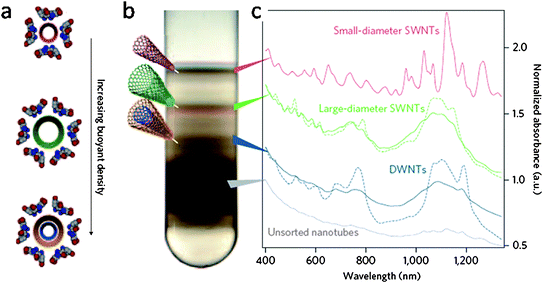 | ||
| Fig. 3 (a) Cartoon of sodium cholate encapsulated carbon nanotubes with different nanotube buoyant density. (b) Photograph of a centrifuge tube following the first iteration of DGU separation. Four sets of bands corresponding to small-diameter SWNTs, large-diameter SWNTs, DWNTs, and a mix of dense MWNTs, carbonaceous impurities and bundles (thick black band) are observed. (c) The optical absorbance spectra of the corresponding bands of material taken from the centrifuge tube at the locations indicated. Dashed lines represent the absorbance of enriched SWNTs and DWNTs produced following a second DGU iteration. Reprinted from ref. 2. | ||
Due to the complex structure and distributions of CNTs, it is often necessary to combine several characterization techniques in order to provide a comprehensive assessment of the quality of CNTs. A straightforward method to characterize individual DWNTs is high-resolution transmission electron microscopy (TEM), which provides information about the diameters of the inner and outerwalls as well as the crystallinity/defects of DWNTs. The purity of DWNTs claimed in most of the references is based on this method by estimating the ratio of DWNTs to the overall number of CNTs investigated. However, TEM is biased towards local areas and crystalline structures; a statistically meaningful result requires collecting a large number of high-resolution images which is time consuming. To characterize DWNTs on a bulk scale, Raman spectroscopy has proven to be an effective method. A typical Raman spectrum of a SWNT sample contains four major peaks:41,50,51 (1) Radial breathing modes (RBM) at low-frequencies; (2) the “D peak” at around 1340 cm−1, due to structural disorder in the graphitic material; (3) the “G peak” at around 1550–1600 cm−1, attributed to the tangential mode (TM) vibrations of the C atoms. The TM contains two different modes: the (a) transverse optic mode (G− band, ∼1570 cm−1), which is a bond-bending mode whose frequency decreases with decreasing nanotube diameter, and the (b) longitudinal optic mode (G+ mode, ∼1590 cm−1), which is a bond-stretching mode with little diameter dependence; (4) the G′ peak at around 2600 cm−1, which is the second order harmonic of the D mode. It has been widely accepted that the frequency of a RBM (ωRBM/cm−1) is inversely proportional to the nanotube diameter (d/nm)1,2,52 and can be expressed as ωRBM = A/d + B, where A and B are constants. For a DWNT, the RBM mode contains two separated peaks corresponding to the inner-tube and the outerwall which can be in the range of 200–400 cm−1 and below 200 cm−1, respectively.2,53
Y. Kim et al. evaluate the purity of DWNTs with respect to SWNTs by carrying out a chemical doping experiment with H2SO4 for a series of SWNTs/DWNTs mixtures of different ratios.54 A relatively large upshift (ca. 16 cm−1) of the TM in SWNTs was observed after dipping the sample in concentrated sulfuric acid for a short time, whereas no change was observed in the frequency of the TM spectra assigned to the outer-tubes of DWNTs. The intensity however is depressed, probably due to the loss of Raman resonance through the modified optical transitions after doping. It was also observed that the intensity of a newly developed Raman line at 2630 cm−1 in the G′ peak increase monotonically with increasing fraction of DWNTs. The G′ peak is split into two peaks for all samples containing DWNTs by the chemical doping. The relatively linear relation between the fraction of DWNTs and the intensity ratio of the two separated peaks allow for qualitative estimation of the ratio of DWNTs to SWNTs. This method is particularly suitable for qualitatively evaluating CNTs with diameters smaller than 2 nm due to the experimental difficulty associated with observing ωRBM below 100 cm−1. However, the result depends on the precise control of the doping level, which can be technically challenging. By using in situ Raman spectroelectrochemistry, L. Dunsch et al. demonstrated that it is also possible to distinguish the inner-tubes of DWNTs from thin SWNTs.55 This is because the inner-tubes of DWNTs exhibit a delayed attenuation of the intensities of their Raman modes as compared to SWNTs of similar diameter, which bleach rapidly upon electrochemical charging. The difference is also reflected by both the splits and shifts of the TM mode for DWNTs but only shifts for SWNTs upon application of high positive potential. These different spectral responses to chemical doping allow the inner-tubes of DWNTs to be differentiated from the SWNTs.
Photoluminescence (PL) is an effective way to characterize SWNTs that are individually dispersed in solution. However, due to the inter-wall interaction (to be discussed in the following section) the inner-tube PL in DWNTs is more complicated than SWNTs. The work on PL will be discussed in section 3.3.
3. The (n,m)2 opportunity
The double wall structure of DWNTs gives rise to interesting mechanical56 and thermal properties57 which can be superior to other carbon nanostructures including SWNTs. A DWNT can have one of four possible electronic configurations with each wall being either semiconductor (S) or metallic (M): S@S, M@S, M@M, and S@M (inner-tube@outer-tube). From the lattice symmetry point of view, the inner-tube and outerwall can be either incommensurate or commensurate. A DWNT is commensurate if the ratio between the unit cell lengths of the inner and outer-tubes is a rational number and incommensurate if the ratio is irrational.58 A commensurate DWNT has a periodical lattice structure while for incommensurate DWNTs the symmetry is broken. Band gap/electronic properties of DWNTs can be severely affected by the inter-wall interactions, which heavily depend on the structural difference and the distance between the inner-tube and the outer-tube. In this section we will also discuss how the chiralities of inner-tubes can be measured by electron microscopy and other techniques. Emphasis will be placed on the controversial topic involving bright fluorescence from semiconducting inner-tubes.3.1. Electronic properties influenced by the interactions between the walls
A DWNT is made of two concentric SWNT-equivalent nanotubes with an inter-wall spacing of 0.33–0.42 nm.59 Each SWNT can be viewed as a sheet of graphene rolled along a chiral vector into a seamless cylinder. The diameter of a nanotubed = Ch/π, and the electronic properties of a nanotube is defined by the chiral index (n,m). A nanotube is metallic when |n-m| is a multiple of three, whereas it is semiconducting otherwise (Fig. 4a). Approximately 2/3 of SWNTs are semiconducting and the rest are metallic. The electronic density of states of a carbon nanotube is dominated by van Hove singularities, which are kinks in the density of states. Metallic nanotubes have a constant density of states in-between the pair of van Hove singularities closest to the Fermi level, while semiconducting nanotubes have a chirality-dependent energy gap that is on the order of 1 eV and spans the region between the van Hove singularities for filled and empty states.60 For semiconducting SWNTs the bandgap varies inversely with diameter. SWNTs with nearly identical diameters can have different electronic properties depending on the chiral vectors. The electronic properties of DWNTs may not be a simple superposition of the electronic properties of inner and outer layer. The inter-wall distance may also affect the electronic properties of a DWNT. Fig. 4b shows a DWNT with an inner semiconducting SWNT and an outer metallic SWNT.
 | ||
Fig. 4 (a) A DWNT contains two concentric SWNTs. Each SWNT is a molecular cylinder conceptually rolled from graphene along a chiral vector. The circumference of the SWNT is determined by its chiral vector  , where (n,m) are integers known as the chiral indices and , where (n,m) are integers known as the chiral indices and and and  are the unit vectors of the graphene lattice. (b) Schematic of a S@M DWNT and its electronic structure. are the unit vectors of the graphene lattice. (b) Schematic of a S@M DWNT and its electronic structure. | ||
Theoretical calculations have been widely applied to study the inter-wall interactions. S. Liang studied the electronic structure of the commensurate DWNTs by tight-binding model and found that the energy band structure of a DWNT is affected by both the inter-wall coupling strength and the DWNT diameter D (mean value of the inner and outer-tube diameters).61 The energy gap of a S@S DWNT decreases with an increase of the inter-wall coupling tp, a constant describing the π-electron hoping between the two walls, in the range of 0 <tp < 0.4 eV. For illustration, the inter-wall coupling of graphite is 0.35 eV corresponding to the distance between layers of 0.344 nm. The inter-wall coupling is inversely proportional to the difference in radius of the two walls. As the diameter increases, the energy gaps of S@S DWNTs decrease quickly and vanish when D>1.5 nm. M@M DWNTs remain gapless, independent of tp and D. This prediction is supported by density functional theory (DFT).62 For a (6,0)@(20,0) M@S DWNT, R. Moradian et al. computed the density of states and band structure of DWNTs using DFT and found that the individual inner and outer-tube remains the same in electronic type but the DWNT behaves metallic overall. Interestingly, decreasing the distance between the walls leads to a change of electronic type based on their calculations. The individual tubes as well as DWNTs in (6,0)@(10,0) and (6,0)@(14,0) DWNTs all became metallic. In the case of S@M DWNTs, all DWNTs investigated, including (8,0)@(21,0), (10,0)@(21,0) and (14,0)@(21,0), exhibit metallic behavior overall. The semiconducting inner-tubes in the (10,0)@(21,0) and (14,0)@(21,0) become metallic, while the two nanotubes in (8,0)@(21,0) exchange their electronic types. Finally, for the S@S DWNTs, if the two walls are far from each other [for example, (8,0)@(20,0)], then the whole DWNT and both walls remain semiconducting. However, for shorter inter-wall distance, e.g. (10,0)@(20,0) and (14,0)@(20,0), DWNTs become metallic. This behavior is possibly due to strong interactions among the 2pz orbitals (perpendicular to the cylindrical wall surface) of the inner and outer SWNTs when the distance is small (<4.7 Å).
By total-energy electronic structure calculations, S. Okada and A. Oshiyama found that a S@S DWNT can have complicated overall electronic properties. For example, for (7,0)@(16,0) the conduction and the valence bands merge, introducing a finite density of states at the Fermi level which makes this S@S DWNT behave as a metal.63 While for (7,0)@(17,0) and (7,0)@(19,0) DWNTs, semimetal characters were found. The metallization of these S@S DWNTs is due to the overlap between the conduction band of the inner-tube and the valence band of the outer-tube. The σ–π rehybridization increases with decreasing tube radius, hence the π and π* states of the inner-tube downshift more than those of the outer-tube resulting in the band overlap. However, it was found that (8,0)@(19,0), (8,0)@(20,0), (10,0)@(19,0), and (10,0)@(20,0) remain as semiconductors with band gaps of 0.26 eV, 0.23 eV, 0.5 eV, and 0.5 eV, respectively. It is thus believed that the metallization of the DWNTs is a consequence from the subtle balance between the curvature difference of the constituent tubes and the σ–π rehybridization of the inner-tube. The electronic structure of a DWNT depends not only on the curvatures of the constituent nanotubes but also on the inter-wall distance. It was found that although the curvature difference monotonically increases for the (7,0)@(17,0), (7,0)@(19,0), and (7,0)@(20,0), the degrees of the band overlaps are almost the same. V. Zólyomi et al. studied the inter-wall interaction in DWNTs by density functional theory and the intermolecular Hückel model. They found that charge transfer between the inner and outer-tubes can occur with an average magnitude ranging from 0.005 to 0.035 electron per Å length along the tube axis.64 They also observed the curvature induced mixing between σ and π bands of the nanotubes. These two combined effects cause a transition from semiconductor to metal for the above DWNTs.
The experimental verification of these theoretical predictions may come from combined electrical transport measurements and structural characterization on the same DWNT. Y. Tison et al. confirmed by scanning tunneling microscopy (STM) and scanning tunneling spectroscopy (STS) measurements that a metallic DWNT can be composed of two semiconducting nanotubes.65STM images of the DWNT show a hexagonal lattice structure with a periodicity of 0.25 ± 0.01 nm, which is similar to those observed on graphite due to an interlayer interaction.66 There are only a few experiments reporting the electrical transport properties of DWNTs.67–69 S. Wang et al. systematically measured 125 DWNT FETs and found that 52 were semiconducting, 44 were metallic, while 29 show neither purely semiconducting nor metallic characteristics.68 These three different types of field-effect characteristics were identified as resulting from S@S, M@M or S@M, and M@S combinations of the two shells of the DWNTs. The S@S type DWNT shows basically the same field-effect characteristics as that of a semiconducting SWNT, and a M@M or S@M type DWNT behaves as a metallic SWNT. The current of a M@S type DWNT FET cannot be completely turned off at all gate voltages. The on/off ratio is typically less than 10 at room temperature, which is far lower than that can be achieved by S@S type DWNT FETs and semiconducting SWNT FETs of similar diameters. The transition region from the hole-conduction region (Vg <10 V) to the electron transport region (Vg >10 V) is much wider than that for S@S type DWNT FETs or SWNT FETs. These observations are attributed to a screening effect by the metallic inner-tube which shields the free charges in the semiconducting outerwall from the gate effect. The screening effect is directly related to the inter-wall interaction, which increases with increasing temperature and tube diameter. X. R. Wang et al. in contrast, attributed the anomalous field-effect characteristic observed in the M@S DWNTs to the proximity effect of a metallic phase.70 The electron wave functions of the inner metallic tube was believed to penetrate into the outer semiconducting tube, generating nonzero local density of states and new conducting channels in the semiconducting tube.
The interactions between the inner and outer-tubes can be observed with Raman spectroscopic techniques. R. Pfeiffer et al. investigated the Raman response of the inner-tube RBMs in DWNTs and found that the number of observed RBMs is two to three times larger than the number of possible nanotubes in the studied frequency range.71 The discrepancy was reconciled by inter-wall interaction-induced splitting of the inner-tube Raman response. F. Villalpando-Paez et al. reported a detailed study of 11 individual C60@SWNT peapod-derived DWNTs with a semiconducting (6,5) inner-tube and various outer metallic tubes.51 A frequency upshift in ωG− was correlated with an upshifted ωRBM for the inner nanotube. An upshifted ωRBM is indicative of smaller wall-to-wall distances and a higher degree of inter-wall interaction. Hence, they attributed the upshift of ωG− to the increasing inter-tube interactions in the DWNTs. The D-band mode can be divided into two components: one low (ωD1) frequency that is related to the inner-tube, and one high (ωD2) frequency that is related to the outer-tube. The lower frequency component ωD1 upshifts with decreasing wall-to-wall distances, while the upper frequency D-band component ωD2 is independent of the wall-to-wall distance. These spectroscopic methods can be applied to study the other three types of DWNT structures and allow opportunities to explore the optical and electronic properties as a function of the inter-wall distance.
3.2. Chirality dependent electronic properties
The electronic property of a SWNT depends sensitively on the chirality.72 For DWNTs, this dependence is even more complex due to the inter-wall interactions. It is important to determine the chirality of DWNTs, both outer and inner-tubes, to establish a direct correlation between chirality and electronic property. To determine the chirality of a CNT, both the diameter and the chiral angle of a nanotube are needed. For a CNT with a diameter between 0.5–2 nm, there are several hundreds of possible chiralities. Thus, high precision measurements must be ensured for a correct assignment of the chirality of CNTs. There are two types of techniques that have been used to determine the chirality of a CNT: The first one is a structural method based on STM or high resolution TEM/selected area electron diffraction (SAED). The second technique is based on spectroscopic measurements such as STS and Raman scattering. The assignment of chirality for SWNTs based on resonant Raman spectroscopy has been demonstrated by several groups; the pioneering work by Dresselhaus' group in particular has established a systematic Raman database for SWNTs.72–75 It is more difficult to assign the chiralities of DWNTs by resonant Raman spectroscopy due to the inter-wall interactions, which affect the RBM frequencies, and the often different excitation windows for the inner and outer-tubes.76 However, by measuring both the inner-tube and outerwall of the same DWNT under resonance conditions, Dresselhaus and co-workers were able to determine the chiralities of three DWNTs.76Both STM and STS have been successfully applied to probe the structure of SWNTs.77,78STM can provide a direct observation of the atomic structure of CNTs, while STS presents well defined and sharp peaks related to van Hove singularities. Because STM is a surface technique, it can only probe the structure of SWNTs or the outer-tube of a DWNT. However, moiré patterns were recently observed by N. Fukui in STM images of DWNTs.79 These local modulations of electronic states are due to the inter-wall interactions and can be used to assign the chiral vector of the inner-tube. The chiralities of DWNTs can also be determined by TEM in conjunction with STM/STS.80 In a reported example, the chirality of an outer-tube is firstly assigned to be (18,10) based on STM measured diameter and chiral angle. The inter-wall spacing is determined by TEM and the inner-tube diameter is in the range of 0.92–1.38 nm, in which there are still 40 possible chiralities. Since experimentally the DWNT shows a nonzero density of states at the Fermi level, they narrow down the possible chiralities of the inner-tube to 14 metallic nanotubes by assuming that the DWNT they studied is incommensurate and the electronic structures of an incommensurate DWNT is the sum of the electronic structures of the inner-tube and outerwall based on the theoretical work of Saito et al.81 By comparison with the calculated electronic density of states, they believed that chirality of the inner-tube is (11,5) or (12,3). A definite structural assignment has yet to be achieved using this technique. It is also important to note that the authors neglect the possibility for a S@S DWNT to behave metallic overall (as discussed in section 3.1.).
Electron diffraction has been demonstrated to be an effective way to determine the chirality of SWNTs.67,82,83 Extending to DWNTs, M. Kociak et al. determined the chiral indices of the inner and outer-tubes of a DWNT by SAED and measured the electrical transport properties of the same DWNT.67 The CNTs were electrically connected to a sample holder that can be manipulated using a piezo controller and a fixed component made of a gold tip with a mercury droplet. The diffraction patterns were acquired when both end connections are visible. A (51,34)@(53,43) structure was determined from the electron diffraction pattern (for how to elucidate structures from electron diffraction patterns, readers are referred to papers by S. Amelinckx, and L. C. Qin et al.82,83). A fitted I–V curve of an exponential law was recorded from 1 to 3 V. It was postulated that only the outer-tube participates in transport at low bias, while some electrons may be able to tunnel from the outer-tube to the inner-tube and contribute to the total transportation at higher bias. The suspended geometry setup avoids the nanotube-substrate effect which causes doping of tubes from the substrate.77 Unfortunately, they only studied one S@S device, probably due to the difficulty associated with device fabrication. This issue is addressed by K. Liu et al. who fabricated DWNT-based field-effect transistors (FETs) on SiO2/Si substrates with mircofabricated 5–20 μm wide slits to enable high resolution TEM studies of the same DWNT.84,85 The electrical properties measured are correlated to the (n,m) indices determined by electron diffraction. A total of 82 DWNTs with different chirality combinations were investigated. No modulation by the gate voltage was found for those with metallic outer-tubes. Fig. 5 shows the electrical transport characteristics of the four types of DWNTs. For M@S DWNTs, the on/off current ratio is less than 20, and the source–drain current can be suppressed by a positive gate voltage but cannot be completely depleted. For S@S DWNTs, a typical p-type semiconducting behavior with an on/off current ratio as high as 104 was observed. Interestingly, no metallic behavior was reported from S@S DWNTs, probably because the large diameter DWNTs that they used are incommensurate. This method could also enable the inner/outer-tube electronic relationship measurement by in situ breaking down of the outer-tubes. The authors measured the transport characteristic of the inner-tube of a S@M DWNT by breaking down the outer-tube with a relatively higher current.
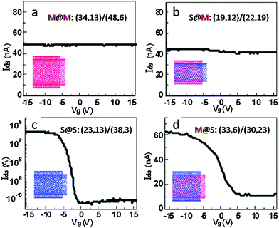 | ||
| Fig. 5 Charge transfer characteristics (current vs. gate-voltage) of the four types of DWNTs: (a) M@M, (b) S@M, (c) S@S, and (d) M@S DWNTs. The drain voltage (Vds) are 4, 4, 100, and 4 mV in panels a, b, c, and d, respectively. Reprinted from ref. 84. | ||
3.3. Does a semiconducting inner-tube fluoresce?
The discovery of exciton fluorescence from isolated semiconducting SWNTs in aqueous suspensions was an important breakthrough in carbon nanotube science.72,86 A nanotube is excited to a higher energy state (e.g. E22) which can relax to the ground state by fluorescent emission at a lower energy approximately matching that of the first transition between van Hove singularities in electronic density of states (E11). Each semiconducting nanotube has a unique pair of E22 and E11. Excitation-emission photoluminescence (PL) mapping can thus unambiguously determine the chirality of a semiconducting SWNT. The excitation range is typically in the range of 400 to 850 nm and the emission covers the near infrared region (∼800–1600 nm).72 However, whether a semiconducting inner-tube within a DWNT will fluoresce has been a subject of debate.2,87–92T. Okazaki et al. reported the PL quenching behavior of peapod-derived DWNTs.88 The DWNTs studied were prepared by annealing C60@SWNT peapods at 1200 °C in vacuum (<10−6 Torr) using SWNTs with diameter of ∼1.2–1.4 nm, which were produced by pulsed laser vaporization. DWNTs were dispersed in D2O containing 1 wt% of sodium dodecylbenzene sulfonate (SDBS) by ultasonication. The dispersion was then centrifuged at 127600 g for 1 h to obtain the supernatant for optical characterization. The PL map shows strong PL peaks in the ranges of 800–950 nm excitation and 1400–1600 nm emission, which corresponds to the ES11 emission from the outer semiconducting tubes with diameter of ∼1.2–1.4 nm. However, no PL signals were observed at ∼598 nm excitation (∼1037 nm emission), which corresponds to the ES22 excitation (ES11 transitions) of the inner-tubes. The authors suggested that the inter-wall distance of a DWNT is an important parameter that governs the PL quantum yield of the DWNT. Such inter-tube interaction may cause a downshift of the energy levels and even closure of the band gap. In their case, the inter-wall distance was estimated to be less than 0.35 nm. It was suggested that a sample containing a significant fraction of DWNTs with larger inter-wall distances could show PL signals.93
In contrast to T. Okazaki's results, H. Muramatsu et al. reported bright PL from the inner-tubes of peapod-derived DWNTs.87 They used arc-discharge produced SWNTs with a diameter of about 1.2–1.3 nm as the fullerene host material and annealed the peapods at a temperature from 1500 to 2000 °C in an argon atmosphere. No PL signals were observed in the excitation range from 500–800 nm for DWNTs annealed at 1600 °C, which is consistent with T. Okazaki's work. Since the presence of inner-tubes was identified using the RBM in Raman spectra for samples annealed at 1500 and 1600 °C, the authors suggested that the lack of a PL signal is due to the metallic behavior of the inner-tubes or due to the formation of intra-molecular junctions in the inner-tubes, where a semiconducting tube is connected to a metallic tube. The formation of such a corrugated metallic structure could happen at a lower temperature (1500 and 1600 °C) resulting in the PL quenching. However, PL signals were observed by annealing the peapods at 1700 and 1800 °C, and the strongest PL signals were obtained from samples annealed at 2000 °C. In these three cases, there is no substantial difference in the inter-wall spacing based on TEM results. Since no incomplete DWNTs with exposed SWNTs (which may occur due to ultrasonication induced cutting) were observed from TEM, the authors attributed the strong PL to the inner-tubes of DWNTs.
The controversy is due to several reasons: (1) A 100% pure sample of DWNTs is thus far not available. SWNTs contaminated in a DWNT sample can contribute to the PL; (2) Even if 100% pure DWNTs are used, the possibility of inner-tubes sliding out from the outer-tubes during ultrasonication and contributing to the observed PL cannot be ruled out; (3) The inter-wall distance varies in different DWNT samples, which can affect the inter-tube interaction, and thus charge transfer from the inner-tube to the outerwall can occur resulting in PL quenching; (4) for peapod-derived DWNTs, defects or disconnection in the inner-tubes will affect the PL.
The debate has become very interesting due to several recent works.2,89,94 M. Endo et al. claimed that the inner-tubes of fluorinated DWNTs fluoresce brightly.94 However, A. Green and M. Hersam observed an 83% attenuation of fluorescence in their DWNT samples, which were highly enriched by density gradient ultracentrifugation.2 D. Tsyboulski and co-workers later provided quantitative, experimental evidence that semiconducting inner-tubes within DWNTs do not fluoresce at all.89 Even if they do, the fluorescence is at least 10000 times weaker compared to SWNTs of the same chirality. They suggest the fluorescence observed by the previous authors92,94 may come from SWNTs that were originally embedded in the bundles or slide out from fluorinated DWNTs due to ultrasonication. In order to clarify the source of PL, D. Tsyboulski et al. prepared samples of purified CVD-grown DWNTs and performed a set of control experiments to reveal the PL properties of inner-tubes. They investigated the susceptibility of DWNT fluorescence to chemical derivatization by exposing surfactant-encapsulated individual CNTs to solutions of a diazonium salt that is known to react with nanotube sidewalls. It has been shown that a low degree of sidewall functionalization (∼1 in 10000 carbon sites) can significantly suppress SWNT fluorescence,95,96 however for DWNTs the inner-tubes should be protected against chemical attacks by the outerwalls. Since fluorescence quenching was rapid and nearly complete after adding the diazonium salt (Fig. 6), the observed PL was attributed to SWNTs rather than inner-tubes of DWNTs. Measurements of individual fluorescent nanotubes show that both the inner-tube within a DWNT and a SWNT of the same chirality have the same emission peak wavelength, line width, and brightness. This result further supports that the emitter could not be the inner-tubes of DWNTs since electronically perturbed inner-tubes by the outer-tubes should show different emission spectra compared to SWNTs.97 The persistence lengths of the emitters in the DWNT samples were found to have the same value as those from SWNT samples, however a much higher value is expected for DWNTs due to the double-wall structure. A final approach they took to clarify the source of the emitters is purification by density gradient ultracentrifugation. Fractions of different densities were collected and analyzed by absorption spectroscopy, fluorescence spectroscopy and high resolution TEM. The topmost fractions 1–4 showed sharp spectral absorption and emission peaks characteristic of SWNTs with diameters in the range of 0.7–1.0 nm, accounting for more than 95% of the sample's total near-IR emission (Fig. 7). Since high-resolution TEM results did not show any presence of DWNTs even for the denser fractions 5–8, the absorptions of these fractions were ascribed to E11 transitions of metallic SWNTs and E22 transitions of semiconducting SWNTs with significantly larger diameters. The emission intensity and absorption at 966 nm (a distinct and intense spectral feature of (8,3) nanotubes) as a function of depth in the centrifuge tube revealed that the fluorescence signal peaks strongly at fractions 2 whereas the absorption reaches a peak near fraction 9 from a higher density region. Fluorescence and absorption data measured on re-centrifuged fractions of 7–10 revealed that 80% of the emission occurred from the top 6 fractions. HR-TEM results show that only fraction 8 and 9 contained DWNTs, while fractions 1–7 contained SWNTs. From these data the fluorescence absorption ratio for combined fractions 7–10 in Fig. 7a is at least a factor of 10,000 lower than that for fraction 2. All these findings support the conclusion that the near-IR emission originates from SWNT impurities rather than from the inner-tubes of pristine DWNTs.
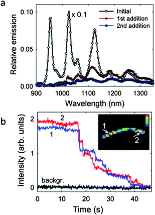 | ||
| Fig. 6 Fluorescence quenching was rapid and nearly complete after adding bromobenzenediazonium salt solution. (a) Fluorescence spectra of a DWNT suspension after addition of bromobenzenediazonium salt solution. (b) Stepwise fluorescence quenching. The inset shows locations of the segments from which emission intensities are measured. Reprinted from ref. 89. | ||
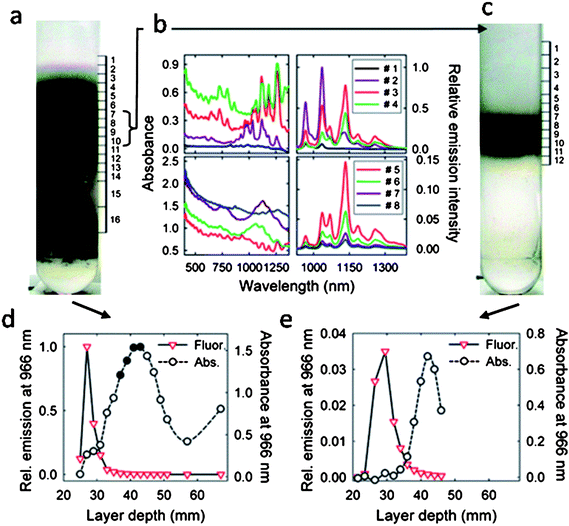 | ||
| Fig. 7 (a) Optical image of the DWNT suspension in a centrifuge tube after density gradient centrifugation. (b) Absorption and fluorescence spectra (excited at 660 nm) of fractions 1–8 collected from the centrifuge tube shown in a. (c) Optical image of a sample containing fractions 7–10 from the first separation after the second step of DGU. (d) Absorbance (circles) and relative emission intensity (triangles), measured at 966 nm, of fractions from the first separation step. (e) Absorbance (circles) and relative emission intensity (triangles), measured at 966 nm, of fractions collected from the tube shown in panel c after second step processing of fractions 7 – 10 (marked as solid circles in (d)) from the first separation step. Reprinted from ref. 89. | ||
Why do semiconducting inner-tubes not fluoresce? This question is open since the debate is not yet settled. Here we provide a simple analysis and suggest experiments to settle this debate. If one assumes each constituent nanotube has a 2/3 probability of being a semiconductor, then on average 1/9 of the DWNT population will be M@M, 2/9 being S@M, 2/9 being M@S, and the remaining 4/9 being S@S. It is known that the PL of a semiconducting SWNT can be efficiently quenched by metallic nanotubes when they are in van der Waal contact (as in a bundle).98 This quenching mechanism can become even more effective in DWNTs since the inner-tube is completely surrounded by the outerwall. For this reason, only the inner-tube within a S@S DWNT has the possibility to fluoresce. However, this quenching mechanism can not fully account for the experimentally observed decrease in fluorescence quantum yield by four orders of magnitude compared to SWNTs,89 since there are still approximately 4/9 of the population that are S@S DWNTs. We postulate that outerwall quenching is the major mechanism. The outerwall has a lower energy level since the bandgap of a semiconducting nanotube is inversely proportional to the nanotube diameter.72 An excited inner-tube can decay by energy transfer or charge transfer to the outerwall. The latter pathway has a possibility to emit, but the fluorescence will occur through the E11 transition of the larger diameter outerwall. This outerwall fluorescence can go undetected since the emission will go beyond the limit of the InGaAs detectors used in these studies. Although this hypothesis has yet to be confirmed, this radiative decay pathway has been observed with bundles of semiconducting SWNTs.99 In light of the theoretical calculations discussed in Section 3.1, some of the S@S DWNTs can have a smaller overall bandgap or even become metallic due to strong inter-wall interactions, and thus no PL will be observed from the inner-tubes of these structures.
Although D. Tsyboulski et al.'s experiments unambiguously proved that semiconducting inner-tubes virtually do not fluoresce, we note that pristine DWNTs are used in their experiments while in Endo et al.'s experiment fluorinated DWNTs are utilized. This structural difference could be important, but remains undifferentiated in follow-up publications.87,94 There is a possibility that fluorinated DWNTs may be different from pristine DWNTs since outerwall functionalization can weaken the inter-wall interactions by electronically breaking down the π-system of the outerwall. However, for fluorinated DWNTs it is difficult to exclude the possibility of extracting the inner-tubes or exfoliating SWNTs originally embedded in bundles due to ultrasonication. Future experiments that enable outerwall selectively functionalized, water soluble DWNTs may allow one to settle this debate. Ongoing experiments in our research group aim to address this problem.
4. Outerwall selective covalent functionalization of DWNTs
DWNTs have the potential to become novel sensors and electronic devices due to their unique double-wall structure. By selectively functionalizing the outerwall, one can control the solubility of a DWNT and its environmental compatibility, while potentially preserving the optical and electronic properties of the inner-tube. All pristine CNTs are insoluble in water and nearly all organic solvents due to collective van der Waals interactions which cause CNTs to form tightly packed bundles. The narrow absorption and emission spectra of individual CNTs become attenuated or absent entirely within a bundled state. CNT bundles are difficult to process physically for electronic applications such as field effect transistors which require precise positioning on a substrate and conductive composites which can have uniformity issues due to inhomogeneous CNT dispersions. Biomedical applications for CNTs as either fluorescent tags or targeted cell-delivery devices have also been hindered by the insolubility issue which would prevent these nanomaterials from distributing effectively throughout the body.Over the past decade, enormous efforts have been devoted to addressing this problem confronting basic and applied research on SWNTs. There are mainly two approaches: covalent sidewall functionalization chemistry and non-covalent processes such as the use of surfactants. Covalent methods are useful for modifying the chemical surface properties of carbon nanotubes to form thermodynamically stable solutions in a variety of solvents, however the conversion of sp2 hybridized carbon of the nanotube wall to sp3 has the side-effect of diminishing and even completely eradicating the desirable electronic and optical properties. It is well-known that covalent sidewall functionalization of SWNTs can drastically change the electronic states of nanotubes near the Fermi level.100,101 Theoretical calculations suggest that an impurity state near the Fermi level is induced after covalent addition of a functional group on the sidewall, and the effect of modification on electronic properties is independent of the choice of functional groups (–COOH, –NH2, –OH, –CH3, –H, –F).101 The electronic state extends over a much larger space (>10 Å) than that of the structural deformation around the functionalization site (5 Å).
Non-covalent methods have no such problem, as the CNT itself is not intrinsically modified - rather the surface is encapsulated in a surfactant or wrapped by polymers which are designed to improve solubility and dispersion of the nanotubes. However, this method is limited by low yields, surfactant contaminations and solution instability. While SWNTs suffer from all of these problems, DWNTs may provide an answer to the covalent/non-covalent modification dilemma. In the following sections, we will discuss the outerwall selective chemistry, including fluorination developed by others and wet chemistry developed in our group. The latter is capable of producing water soluble DWNTs, while maintaining high electrical conductivity due to the intact inner-tube pathways.
Fluorination is an effective chemistry for functionalizing SWNTs102–105 and has been recently applied to DWNTs. H. Muramatsu et al. demonstrated that DWNTs were fluorinated by directly reacting with fluorine gas at 200 °C.106 The RBMs of the outerwalls were clearly depressed after fluorination. XPS revealed that the stoichiometry of the fluorinated DWNTs is CF0.30, and HR-TEM showed that the double-layered structure is sustained after fluorination. L. Bulusheva et al. compared the stability of fluorinated DWNTs produced by three different fluorinatation methods: fluorine gas, gaseous BrF3, and plasma (CF4).107 The fluorination of DWNTs by fluorine gas was conducted at 200 °C for 10 min. Fluorination by gaseous BrF3 was done by holding a DWNT sample over a solution of Br2 and BrF3 for 7 days. Plasma fluorination was performed by exposing DWNTs to a CF4 plasma for 10 min at 13.56 MHz and 15 W. The fluorine ratios on the outerwalls of the fluorinated DWNTs are CF0.44, CF0.27, and CF0.21 for samples fluorinated by F2, BrF3, and CF4 plasma, respectively. The lower F concentration obtained from sample prepared by plasma was explained by the restricted penetration of active species due to the formation of a thin fluorinated layer, which blocked the DWNTs within bundles from the reaction. Thermal annealing results show that the defluorination process depends strongly on the method of DWNT fluorination. For DWNTs fluorinated by F2 or BrF3, the fluorine atoms withdraw together with carbon atoms, creating vacancies and edge-sites. While for DWNTs fluorinated by CF4 plasma, only negligible etching of the DWNT outerwall was detected. The defect sites created by defluorination was believed to be responsible for the dissociation of water molecules. These defect sites may allow opportunities for further functionalization.
A common problem with covalent sidewall chemistry is the unattractive tradeoff between solubility and functionality. Covalent functionalization of carbon nanotubes is one of the most promising methods of improving solubility and processing for various uses such as biomedical applications. Unfortunately, covalent addition to the nanotube sidewalls disrupts the π-electron system, causing the loss of the valuable optical and electrical properties associated with SWNTs. However, by outerwall selective covalent chemistry, the solubility of DWNTs can be drastically improved. The outerwall can also serve as a protective barrier to prevent endohedral reactions, potentially allowing the inner-tube to retain its electronic properties.
We have recently shown that outerwall selectively oxidized double-walled carbon nanotubes (oso-DWNTs) are both water soluble and capable of retaining the electrical conductivity of the inner-tube.108 Briefly, DWNTs were exfoliated in oleum (100% H2SO4 with excess SO3) and then reacted with nitric acid to decorate the DWNT with carboxylic acid groups, as confirmed by X-ray photoelectron spectroscopy (XPS). Outerwall selectivity was evident by Raman spectroscopy and HR-TEM. Because the radial breathing modes (RBMs) are inversely proportional to nanotube diameter, it is possible to identify the larger diameter outerwall as producing the RBM signal at approximately 150 cm−1. The inner-tube RBM occurs at a higher frequency due to its smaller diameter, in this case at approximately 215 cm−1. The selective oxidation of outerwalls is shown by the nearly complete depression of the outerwall RBMs while retaining the inner-tube intensity (Fig. 8). This change correlates with the simultaneous decrease of the G band and the rise of the D band, confirming selective oxidative functionalization of the outerwall. Conditions resulting in the highest outerwall selectivity was determined using the ratio of the inner-tube RBM and the G-band: oxidizing 50 mg DWNTs with 10 mL nitric acid over 2 h resulted in the largest ratio of the inner-tube RBM to G-band which indicates the highest degree of functionalization with the greatest retention of the inner-tube. A water solubility of 760 mg/mL was obtained by reacting the DWNTs with 5 mL of nitric acid over 24 h which was the most soluble sample, however increased water-solubility was also concomitant with lower outerwall selectivity and increased oxidative cutting of the DWNTs. Though the 10 mL 2 h sample featuring the highest outerwall selectivity was not the most water soluble, it still demonstrated a high water solubility of approximately 600 mg/mL.
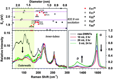 | ||
| Fig. 8 Outerwall selectivity of oxidized DWNTs is shown using Raman spectroscopy. DWNTs were oxidized using a combination of oleum and HNO3 under different reaction conditions. The red line corresponds to 10 mL HNO3 reacted over 2 h, the blue line using 20 mL for 2 h and the green line with 5 mL for 24 h. The raw, non-oxidizded DWNT sample is shown by the black line. The spectra intensities were normalized to the inner-tubes at approximately 215 cm−1 and the shaded region indicates the outerwalls. Metallic inner-tubes correspond to the red-dots in the above Kataura plot in which an excitation of 632.8 nm was used. Reprinted from ref. 108. | ||
Electrical conductivity measurements showed that the conductivity of oxidized DWNTs was retained by 66% better compared to SWNTs. Optimizing the oxidative reaction parameters is expected to further improve conductivity retention of oso-DWNTs. Electrical percolation is attributed to the intact inner-tubes of oso-DWNTs, which provide a continuous conductive pathway through the DWNT thin film by electrical contact with non-functionalized regions of the outerwall (Fig. 9). Retention of partially intact segments of the outerwall after oxidation is necessary to allow conductive inner-tubes pathways to “hopscotch” between the walls of neighboring DWNTs and ultimately through the entire device. CNT devices without this percolating ability will find their electrical current impeded by overly functionalized surfaces that are insulative – decreasing the device efficiency and squandering the conductive properties of the nanotubes. Covalently functionalized SWNTs become increasingly insulative and electrical percolation through the device decreases as non-conducting tubes isolate SWNTs that may still partially retain some electrical properties.
 | ||
| Fig. 9 Intact inner-tubes and limited regions of outerwall non-functionalization enable electrical percolation of oso-DWNTs. (a) SWNTs after sidewall functionalization have an interrupted electrical conduction pathway. (b) Intact inner-tubes form electrically conductive pathways through non-functionalized regions of the outerwall. (c) HR-TEM image featuring two oso-DWNTs. Reprinted from ref. 108. | ||
Effective electrical percolation through a DWNT film is an interesting characteristic for the incorporation of these materials into various applications such as conductive composites, photovoltaics and energy storage devices. The ability to control chemical functionality through the outerwall facilitates solution processing of DWNTs for these applications by improving dispersion and solubility which are necessary for high-throughput printing of CNT electrodes and solar cells. This double-wall chemical strategy allows us to tailor the outerwall for functionality purposes while maintaining the low-dimensional carbon properties of the inner-tube. The applications of this unique property will be discussed further in the following section.
5. Applications, challenges, and outlook
Double-walled carbon nanotubes have emerged as a new material. Compared to SWNTs, DWNTs have higher mechanical strength and better thermal and chemical stability. The unique double-wall structure allows the outerwall to be selectively functionalized while maintaining an intact inner-tube. Although applications are still in the infancy stage, proof-of-concepts experiments indicate that DWNTs may find applications in areas such as capacitors,109–111 solar cells,112,113 field effect transistors,69,114,115 ultra-fast optical switches,116 mass sensors,117 and nanomotor/nanobearing.118–122 The possibility of DWNTs acting as molecular motor is attributed to the small inter-wall resistance of DWNTs, in which a rotation or slide between the inner and outer shells of DWNTs can be easily performed.121,123,124 A demonstration of the world's smallest motor based on a MWNT has been performed by A. Zettl's group.120 DWNTs can push this limit even further since they only have two walls, exactly what are needed to carry out this basic function of operation. The low-friction interaction between inner and outerwalls also made it possible to fabricate telescopic devices, such as gigahertz oscillators, in which the repeated extension and retraction can be performed by the van der Waals interactions between two concentric tubes.123,125–128 Researchers at Tsinghua University reported that heat flux may also actuate the relative motion of DWNTs.129 Using molecular dynamics simulations, they found that a thermal gradient can be used to drive the relative motion of DWNTs. The thermal driving force through a stationary scheme is on the order of pico-Newtons for a temperature gradient of 1 K nm−1. The final velocity of the relative motion can be on the order of 100 m s−1. The study also suggests that the motion trace depends on both the chirality pair and system temperature. Z. Li et al. found that DWNTs have better transparency-conductance performance as compared with SWNTs and MWNTs.130 This was explained by the fact that SWNT materials contain many semiconducting nanotubes, while MWNTs absorb more photons per nanotube due to larger mass density. A. Zettl et al. reported a new mass sensor nanoelectromechanical system consisting of a DWNT, which provides uniform electrical properties and increased rigidity.117 By measuring the resonant frequency change, which is proportional to the mass of the atom or molecule, the sensor was able to weigh individual gold atoms. B. Liu et al. proposed a novel biomimetic channels based on DWNTs, in which the shielding of the modified DWNTs with amphiphilic outer layer could guarantee biocompatibility of the channel and protect the inner-tube (functional part) from chemical disturbance.131 They found that a DWNT embedded membrane shows good biocompatibility and the ability to function as aquaporins, which are a family of membrane channel proteins that are able to facilitate water permeation but exclude proton leakage. These interesting demonstrations indicate that DWNTs can be more advantageous compared to SWNTs and MWNTs in a variety of applications.Challenging issues confronting the next step of development include how to purify DWNTs by chirality. Density gradient ultracentrifugation has proven to be a powerful tool for the separation of DWNTs from other carbon nanostructures and separation of SWNTs by structure. However, the prospects of large scale separation is not yet clear. Separation by chirality will become exceedingly challenging as the wall number increases. At the same time, it is important to control the selective growth of DWNTs; realizing the ultimate goal of controlling CNT chirality during synthesis142,143 will be the enabling technology for a wide variety of potential applications proposed for CNTs. Raman spectroscopy is an effective way to characterize the properties of DWNTs and can be used for the qualitative evaluation of the purity of DWNTs. Photoluminescence study of the inner-tube of DWNTs has created hot debate over the past several years. Outerwall selective chemistry and theoretical modeling could help to resolve this controversial topic. The outerwall selective chemistry is an effective way to functionalize the outerwall of DWNTs while preserving the properties of inner-tubes. Issues concerning how to precisely control the outerwall chemistry and how the degree of functionalization affects the properties of DWNTs are important. For the application of DWNTs in electronic devices, it is important to assemble DWNTs into ordered arrays or functional structures. These challenges are often shared with SWNTs and graphene. Source of CNTs (synthesis methods) and the sample quality (purity, length, diameter, inter-wall distance, and defect density) should be considered when comparing the literature results. The merits of superior thermal and mechanical properties of DWNTs with outerwall selective chemistry could make DWNTs an excellent additive/enhancement material for composite materials. However, so far most of the applications of DWNT are based on its mechanical properties. Applications based on optical properties lack exploration but will likely become promising directions due to the possibility of simultaneously controlling both the electronic properties and surface chemistry through outerwall selective chemistry.
Acknowledgements
We thank Y. Zhang and Y. M. Piao for helpful discussions. This work was supported by startup funds and a General Research Board Research Support Award from the University of Maryland, and a Doctoral New Investigator award from the ACS Petroleum Research Fund. Y.H.W. was partially supported as part of the Science of Precision Multifunctional Nanostructures for Electrical Energy Storage, an Energy Frontier Research Center funded by the U.S. Department of Energy, Office of Science, Office of Basic Energy Sciences under Award Number DESC0001160. A.H.B. acknowledges support from the Department of Energy Office of Science Graduate Fellowship.References
- M. Endo, H. Muramatsu, T. Hayashi, Y. A. Kim, M. Terrones and N. S. Dresselhaus, Nature, 2005, 433, 476 CrossRef CAS.
- A. A. Green and M. C. Hersam, Nat. Nanotechnol., 2009, 4, 64 CrossRef CAS.
- S. Iijima, Nature, 1991, 354, 56 CrossRef CAS.
- T. W. Ebbesen and P. M. Ajayan, Nature, 1992, 358, 220 CrossRef CAS.
- J. L. Hutchison, N. A. Kiselev, E. P. Krinichnaya, A. V. Krestinin, R. O. Loutfy, A. P. Morawsky, V. E. Muradyan, E. D. Obraztsova, J. Sloan, S. V. Terekhov and D. N. Zakharov, Carbon, 2001, 39, 761 CrossRef CAS.
- Y. Saito, T. Nakahira and S. Uemura, J. Phys. Chem. B, 2003, 107, 931 CrossRef CAS.
- B. Ha, D. H. Shin, J. Park and C. J. Lee, J. Phys. Chem. C, 2008, 112, 430 CrossRef CAS.
- H. J. Huang, H. Kajiura, S. Tsutsui, Y. Murakami and M. Ata, J. Phys. Chem. B, 2003, 107, 8794 CrossRef CAS.
- H. X. Qiu, Z. J. Shi, L. H. Guan, L. P. You, M. Gao, S. L. Zhang, J. S. Qiu and Z. N. Gu, Carbon, 2006, 44, 516 CrossRef CAS.
- H. Yoshida, T. Sugai and H. Shinohara, J. Phys. Chem. C, 2008, 112, 19908 CrossRef CAS.
- B. W. Smith, M. Monthioux and D. E. Luzzi, Nature, 1998, 396, 323 CrossRef CAS.
- B. W. Smith, M. Monthioux and D. E. Luzzi, Chem. Phys. Lett., 1999, 315, 31 CrossRef CAS.
- R. Pfeiffer, H. Peterlik, H. Kuzmany, H. Shiozawa, A. Gruneis, T. Pichler and H. Kataura, Phys. Status Solidi B, 2007, 244, 4097 CrossRef CAS.
- R. Pfeiffer, M. Holzweber, H. Peterlik, H. Kuzmany, Z. Liu, K. Suenaga and H. Kataura, Nano Lett., 2007, 7, 2428 CrossRef CAS.
- S. Bandow, M. Takizawa, K. Hirahara, M. Yudasaka and S. Iijima, Chem. Phys. Lett., 2001, 337, 48 CrossRef CAS.
- P. Launois, M. Chorro, B. Verberck, P. A. Albouy, S. Rouziere, D. Colson, A. Forget, L. Noe, H. Kataura, M. Monthioux and J. Cambedouzou, Carbon, 2010, 48, 89 CrossRef CAS.
- S. Bandow, K. Hirahara, T. Hiraoka, G. Chen, P. Eklund and S. Iijima, MRS Bull., 2004, 29, 260 CAS.
- T. P. Rudolf Pfeiffer, Yoong Ahm Kim, Hans Kuzmany, Double-Wall Carbon Nanotubes, ed. G. D. A. Jorio, M. S. Dresselhaus, Springer-Verlag, 2008 Search PubMed.
- J. H. Hafner, M. J. Bronikowski, B. R. Azamian, P. Nikolaev, A. G. Rinzler, D. T. Colbert, K. A. Smith and R. E. Smalley, Chem. Phys. Lett., 1998, 296, 195 CrossRef CAS.
- E. Flahaut, A. Peigney, C. Laurent and A. Rousset, J. Mater. Chem., 2000, 10, 249 RSC.
- H. Qi, C. Qian and J. Liu, Nano Lett., 2007, 7, 2417 CrossRef CAS.
- J. Q. Wei, L. J. Ci, B. Jiang, Y. H. Li, X. F. Zhang, H. W. Zhu, C. L. Xu and D. H. Wu, J. Mater. Chem., 2003, 13, 1340 RSC.
- W. Z. Li, J. G. Wen, M. Sennett and Z. F. Ren, Chem. Phys. Lett., 2003, 368, 299 CrossRef CAS.
- J. Q. Huang, Q. Zhang, M. Q. Zhao and F. Wei, Nano Res., 2009, 2, 872 CrossRef CAS.
- J. Q. Wei, B. Jiang, D. H. Wu and B. Q. Wei, J. Phys. Chem. B, 2004, 108, 8844 CrossRef CAS.
- T. Hiraoka, T. Kawakubo, J. Kimura, R. Taniguchi, A. Okamoto, T. Okazaki, T. Sugai, Y. Ozeki, M. Yoshikawa and H. Shinohara, Chem. Phys. Lett., 2003, 382, 679 CrossRef CAS.
- P. Ramesh, T. Okazaki, R. Taniguchi, J. Kimura, T. Sugai, K. Sato, Y. Ozeki and H. Shinohara, J. Phys. Chem. B, 2005, 109, 1141 CrossRef CAS.
- G. Q. Ning, Y. Liu, F. Wei, Q. Wen and G. H. Luo, J. Phys. Chem. C, 2007, 111, 1969 CrossRef CAS.
- J. Cumings, W. Mickelson and A. Zettl, Solid State Commun., 2003, 126, 359 CrossRef CAS.
- M. R. Maschmann, A. D. Franklin, P. B. Amama, D. N. Zakharov, E. A. Stach, T. D. Sands and T. S. Fisher, Nanotechnology, 2006, 17, 3925 CrossRef CAS.
- Y. Y. Zhang, J. M. Gregoire, R. B. van Dover and A. J. Hart, J. Phys. Chem. C, 2010, 114, 6389 CrossRef CAS.
- D. N. Futaba, J. Goto, S. Yasuda, T. Yamada, M. Yumura and K. Hata, J. Am. Chem. Soc., 2009, 131, 15992 CrossRef CAS.
- D. N. Futaba, J. Goto, S. Yasuda, T. Yamada, M. Yumura and K. Hata, Adv. Mater., 2009, 21, 4811 CrossRef CAS.
- D. N. Futaba, K. Hata, T. Namai, T. Yamada, K. Mizuno, Y. Hayamizu, M. Yumura and S. Iijima, J. Phys. Chem. B, 2006, 110, 8035 CrossRef CAS.
- D. N. Futaba, K. Hata, T. Yamada, K. Mizuno, M. Yumura and S. Iijima, Phys. Rev. Lett., 2005, 95, 056104 CrossRef.
- K. Hata, D. N. Futaba, K. Mizuno, T. Namai, M. Yumura and S. Iijima, Science, 2004, 306, 1362 CrossRef CAS.
- T. Yamada, T. Namai, K. Hata, D. N. Futaba, K. Mizuno, J. Fan, M. Yudasaka, M. Yumura and S. Iijima, Nat. Nanotechnol., 2006, 1, 131 CrossRef CAS.
- R. H. Baughman, Nat. Nanotechnol., 2006, 1, 94 CrossRef CAS.
- D. Kondo, S. Sato, A. Kawabata and Y. Awano, Nanotechnology, 2008, 19, 435601 CrossRef.
- Y. A. Kim, H. Muramatsu, T. Hayashi, M. Endo, M. Terrones and M. S. Dresselhaus, Chem. Vap. Deposition, 2006, 12, 327 CrossRef CAS.
- P. J. F. Harris, Carbon Nantoube Science: Synthesis, Properties and Applications, Cambridge University Press, 2009 Search PubMed.
- M. Terrones, Int. Mater. Rev., 2004, 49, 325 Search PubMed.
- L. Ci, R. Vajtai and P. M. Ajayan, J. Phys. Chem. C, 2007, 111, 9077 CrossRef CAS.
- C. L. Cheung, A. Kurtz, H. Park and C. M. Lieber, J. Phys. Chem. B, 2002, 106, 2429 CrossRef CAS.
- V. K. Kayastha, S. Wu, J. Moscatello and Y. K. Yap, J. Phys. Chem. C, 2007, 111, 10158 CrossRef.
- G. D. Nessim, A. J. Hart, J. S. Kim, D. Acquaviva, J. H. Oh, C. D. Morgan, M. Seita, J. S. Leib and C. V. Thompson, Nano Lett., 2008, 8, 3587 CrossRef CAS.
- B. Zhao, D. N. Futaba, S. Yasuda, M. Akoshima, T. Yamada and K. Hata, ACS Nano, 2009, 3, 108 CrossRef CAS.
- T. Sugai, H. Yoshida, T. Shimada, T. Okazaki and H. Shinohara, Nano Lett., 2003, 3, 769 CrossRef CAS.
- N. Kishi, T. Hiraoka, P. Ramesh, J. Kimura, K. Sato, Y. Ozeki, M. Yoshikawa, T. Sugai and H. Shinohara, Jpn. J. Appl. Phys., 2007, 46, 1797 CrossRef CAS.
- S. Piscanec, M. Lazzeri, J. Robertson, A. C. Ferrari and F. Mauri, Phys. Rev. B: Condens. Matter Mater. Phys., 2007, 75, 035427 CrossRef.
- F. Villalpando-Paez, H. Muramatsu, Y. A. Kim, H. Farhat, M. Endo, M. Terrones and M. S. Dresselhaus, Nanoscale, 2010, 2, 406 RSC.
- S. Bandow, G. Chen, G. U. Sumanasekera, R. Gupta, M. Yudasaka, S. Iijima and P. C. Eklund, Phys. Rev. B: Condens. Matter Mater. Phys., 2002, 66, 075416 CrossRef.
- R. Pfeiffer, F. Simon, H. Kuzmany and V. N. Popov, Phys. Rev. B: Condens. Matter Mater. Phys., 2005, 72, 161404 CrossRef.
- Y. A. Kim, H. Muramatsu, M. Kojima, T. Hayashi, M. Endo, M. Terrones and M. S. Dresselhaus, Chem. Phys. Lett., 2006, 420, 377 CrossRef CAS.
- M. Kalbac, L. Kavan and L. Dunsch, Anal. Chem., 2007, 79, 9074 CrossRef CAS.
- B. Peng, M. Locascio, P. Zapol, S. Y. Li, S. L. Mielke, G. C. Schatz and H. D. Espinosa, Nat. Nanotechnol., 2008, 3, 626 CrossRef CAS.
- Y. A. Kim, H. Muramatsu, T. Hayashi, M. Endo, M. Terrones and M. S. Dresselhaus, Chem. Phys. Lett., 2004, 398, 87 CrossRef CAS.
- M. Damnjanovic, I. Milosevic, T. Vukovic and R. Sredanovic, Phys. Rev. B: Condens. Matter Mater. Phys., 1999, 60, 2728 CrossRef CAS.
- Y. J. Li, K. L. Wang, J. Q. Wei, Z. Y. Gu, Z. C. Wang, J. B. Luo and D. H. Wu, Carbon, 2005, 43, 31 CrossRef CAS.
- M. C. Hersam, Nat. Nanotechnol., 2008, 3, 387 CrossRef.
- S. D. Liang, Phys. B, 2004, 352, 305 CrossRef CAS.
- R. Moradian, S. Azadi and H. Refii-Tabar, J. Phys.: Condens. Matter, 2007, 19, 176209 CrossRef.
- S. Okada and A. Oshiyama, Phys. Rev. Lett., 2003, 91, 216801 CrossRef.
- V. Zolyomi, J. Koltai, A. Rusznyak, J. Kuerti, A. Gali, F. Simon, H. Kuzmany, A. Szabados and P. R. Surjan, Phys. Rev. B: Condens. Matter Mater. Phys., 2008, 77, 245403 CrossRef.
- Y. Tison, C. E. Giusca, V. Stolojan, Y. Hayashi and S. R. P. Silva, Adv. Mater., 2008, 20, 189 CrossRef.
- M.-H. Whangbo and S. N. Magonov, Surface Analysis with STM and AFM, Wenheim, VCH, 1996 Search PubMed.
- M. Kociak, K. Suenaga, K. Hirahara, Y. Saito, T. Nakahira and S. Iijima, Phys. Rev. Lett., 2002, 89, 155501 CrossRef CAS.
- S. Wang, X. L. Liang, Q. Chen, Z. Y. Zhang and L. M. Peng, J. Phys. Chem. B, 2005, 109, 17361 CrossRef CAS.
- T. Shimada, T. Sugai, Y. Ohno, S. Kishimoto, T. Mizutani, H. Yoshida, T. Okazaki and H. Shinohara, Appl. Phys. Lett., 2004, 84, 2412 CrossRef CAS.
- J. Lu, S. Yin, L. M. Peng, Z. Z. Sun and X. R. Wang, Appl. Phys. Lett., 2007, 90, 052109 CrossRef.
- R. Pfeiffer, C. Kramberger, F. Simon, H. Kuzmany, V. N. Popov and H. Kataura, Eur. Phys. J. B, 2004, 42, 345 CrossRef CAS.
- S. M. Bachilo, M. S. Strano, C. Kittrell, R. H. Hauge, R. E. Smalley and R. B. Weisman, Science, 2002, 298, 2361 CrossRef CAS.
- S. Bandow, S. Asaka, Y. Saito, A. M. Rao, L. Grigorian, E. Richter and P. C. Eklund, Phys. Rev. Lett., 1998, 80, 3779 CrossRef CAS.
- R. R. Bacsa, A. Peigney, C. Laurent, P. Puech and W. S. Bacsa, Phys. Rev. B, 2002, 65.
- A. G. Souza, S. G. Chou, G. G. Samsonidze, G. Dresselhaus, M. S. Dresselhaus, L. An, J. Liu, A. K. Swan, M. S. Unlu, B. B. Goldberg, A. Jorio, A. Gruneis and R. Saito, Phys. Rev. B: Condens. Matter Mater. Phys., 2004, 69, 115428 CrossRef.
- F. Villalpando-Paez, H. Son, D. Nezich, Y. P. Hsieh, J. Kong, Y. A. Kim, D. Shimamoto, H. Muramatsu, T. Hayashi, M. Endo, M. Terrones and M. S. Dresselhaus, Nano Lett., 2008, 8, 3879 CrossRef CAS.
- J. W. G. Wildoer, L. C. Venema, A. G. Rinzler, R. E. Smalley and C. Dekker, Nature, 1998, 391, 59 CrossRef CAS.
- T. W. Odom, J. L. Huang, P. Kim and C. M. Lieber, Nature, 1998, 391, 62 CrossRef CAS.
- N. Fukui, Y. Suwa, H. Yoshida, T. Sugai, S. Heike, M. Fujimori, Y. Terada, T. Hashizume and H. Shinohara, Phys. Rev. B: Condens. Matter Mater. Phys., 2009, 79, 125402 CrossRef.
- C. E. Giusca, Y. Tison, V. Stolojan, E. Borowiak-Palen and S. R. P. Silva, Nano Lett., 2007, 7, 1232 CrossRef CAS.
- R. Saito, M. Fujita, G. Dresselhaus and M. S. Dresselhaus, Appl. Phys. Lett., 1992, 60, 2204 CrossRef CAS.
- S. Amelinckx, A. Lucas and P. Lambin, Rep. Prog. Phys., 1999, 62, 1471 CrossRef CAS.
- L. C. Qin, Rep. Prog. Phys., 2006, 69, 2761 CrossRef.
- K. H. Liu, W. L. Wang, Z. Xu, X. D. Bai, E. G. Wang, Y. G. Yao, J. Zhang and Z. F. Liu, J. Am. Chem. Soc., 2009, 131, 62 CrossRef CAS.
- K. H. Liu, Z. Xu, W. L. Wang, P. Gao, W. Y. Fu, X. D. Bai and E. G. Wang, J. Phys. D: Appl. Phys., 2009, 42, 125412 CrossRef.
- M. J. O'Connell, S. M. Bachilo, C. B. Huffman, V. C. Moore, M. S. Strano, E. H. Haroz, K. L. Rialon, P. J. Boul, W. H. Noon, C. Kittrell, J. P. Ma, R. H. Hauge, R. B. Weisman and R. E. Smalley, Science, 2002, 297, 593 CrossRef CAS.
- H. Muramatsu, T. Hayashi, Y. A. Kim, D. Shimamoto, M. Endo, V. Meunier, B. G. Sumpter, M. Terrones and M. S. Dresselhaus, Small, 2009, 5, 2678 CrossRef CAS.
- T. Okazaki, S. Bandow, G. Tamura, Y. Fujita, K. Iakoubovskii, S. Kazaoui, N. Minami, T. Saito, K. Suenaga and S. Iijima, Phys. Rev. B: Condens. Matter Mater. Phys., 2006, 74, 153404 CrossRef.
- D. A. Tsyboulski, Y. Hou, N. Fakhri, S. Ghosh, R. Zhang, S. M. Bachilo, M. Pasquali, L. W. Chen, J. Liu and R. B. Weisman, Nano Lett., 2009, 9, 3282 CrossRef CAS.
- T. Hertel, A. Hagen, V. Talalaev, K. Arnold, F. Hennrich, M. Kappes, S. Rosenthal, J. McBride, H. Ulbricht and E. Flahaut, Nano Lett., 2005, 5, 511 CrossRef CAS.
- K. Iakoubovskii, N. Minami, T. Ueno, S. Kazaoui and H. Kataura, J. Phys. Chem. C, 2008, 112, 11194 CrossRef CAS.
- D. Shimamoto, H. Muramatsu, T. Hayashi, Y. A. Kim, M. Endo, J. S. Park, R. Saito, M. Terrones and M. S. Dresselhaus, Appl. Phys. Lett., 2009, 94, 083106 CrossRef.
- W. C. Ren, F. Li, J. A. Chen, S. Bai and H. M. Cheng, Chem. Phys. Lett., 2002, 359, 196 CrossRef CAS.
- T. Hayashi, D. Shimamoto, Y. A. Kim, H. Muramatsu, F. Okino, H. Touhara, T. Shimada, Y. Miyauchi, S. Maruyama, M. Terrones, M. S. Dresselhaus and M. Endo, ACS Nano, 2008, 2, 485 CrossRef CAS.
- G. Dukovic, B. E. White, Z. Y. Zhou, F. Wang, S. Jockusch, M. L. Steigerwald, T. F. Heinz, R. A. Friesner, N. J. Turro and L. E. Brus, J. Am. Chem. Soc., 2004, 126, 15269 CrossRef CAS.
- L. Cognet, D. A. Tsyboulski, J. D. R. Rocha, C. D. Doyle, J. M. Tour and R. B. Weisman, Science, 2007, 316, 1465 CrossRef CAS.
- D. A. Tsyboulski, E. L. Bakota, L. S. Witus, J. D. R. Rocha, J. D. Hartgerink and R. B. Weisman, J. Am. Chem. Soc., 2008, 130, 17134 CrossRef CAS.
- T. J. McDonald, C. Engtrakul, M. Jones, G. Rumbles and M. J. Heben, J. Phys. Chem. B, 2006, 110, 25339 CrossRef CAS.
- J. Crochet, M. Clemens and T. Hertel, J. Am. Chem. Soc., 2007, 129, 8058 CrossRef.
- J. L. Bahr, J. P. Yang, D. V. Kosynkin, M. J. Bronikowski, R. E. Smalley and J. M. Tour, J. Am. Chem. Soc., 2001, 123, 6536 CrossRef CAS.
- J. J. Zhao, H. K. Park, J. Han and J. P. Lu, J. Phys. Chem. B, 2004, 108, 4227 CrossRef CAS.
- E. T. Mickelson, C. B. Huffman, A. G. Rinzler, R. E. Smalley, R. H. Hauge and J. L. Margrave, Chem. Phys. Lett., 1998, 296, 188 CrossRef CAS.
- S. Kawasaki, K. Komatsu, F. Okino, H. Touhara and H. Kataura, Phys. Chem. Chem. Phys., 2004, 6, 1769 RSC.
- E. T. Mickelson, I. W. Chiang, J. L. Zimmerman, P. J. Boul, J. Lozano, J. Liu, R. E. Smalley, R. H. Hauge and J. L. Margrave, J. Phys. Chem. B, 1999, 103, 4318 CrossRef CAS.
- Z. Gu, H. Peng, R. H. Hauge, R. E. Smalley and J. L. Margrave, Nano Lett., 2002, 2, 1009 CrossRef CAS.
- H. Muramatsu, Y. A. Kim, T. Hayashi, M. Endo, A. Yonemoto, H. Arikai, F. Okino and H. Touhara, Chem. Commun., 2005, 2002 RSC.
- Y. V. F. L. G. Bulusheva, A. V. Okotrub, E. Flahaut, I. P. Asanov, V. O. Koroteev, A. Yaya, C. P. Ewels, A. L. Chuvilin, A. Felten, G. Van Lier and D. V. Vyalikh, Chem. Mater., 2010, 22, 4197 CrossRef.
- A. H. Brozena, J. Moskowitz, B. Y. Shao, S. L. Deng, H. W. Liao, K. J. Gaskell and Y. H. Wang, J. Am. Chem. Soc., 2010, 132, 3932 CrossRef CAS.
- L. Cooper, H. Amano, M. Hiraide, S. Houkyou, I. Y. Jang, Y. J. Kim, H. Muramatsu, J. H. Kim, T. Hayashi, Y. A. Kim, M. Endo and M. S. Dresselhaus, Appl. Phys. Lett., 2009, 95, 233104 CrossRef.
- I. Y. Jang, H. Muramatsu, K. C. Park, Y. J. Kim and M. Endo, Electrochem. Commun., 2009, 11, 719 CrossRef CAS.
- G. G. Chen, S. Bandow, E. R. Margine, C. Nisoli, A. N. Kolmogorov, V. H. Crespi, R. Gupta, G. U. Sumanasekera, S. Iijima and P. C. Eklund, Phys. Rev. Lett., 2003, 90, 257403 CrossRef.
- Y. Jia, J. Q. Wei, K. L. Wang, A. Y. Cao, Q. K. Shu, X. C. Gui, Y. Q. Zhu, D. M. Zhuang, G. Zhang, B. B. Ma, L. D. Wang, W. J. Liu, Z. C. Wang, J. B. Luo and D. Wu, Adv. Mater., 2008, 20, 4594 CrossRef CAS.
- Q. K. Shu, J. Q. Wei, K. L. Wang, H. W. Zhu, Z. Li, Y. Jia, X. C. Gui, N. Guo, X. M. Li, C. R. Ma and D. H. Wu, Nano Lett., 2009, 9, 4338 CrossRef CAS.
- S. D. Wang and M. Grifoni, Phys. Rev. B: Condens. Matter Mater. Phys., 2007, 76, 033413 CrossRef.
- T. Shimizu, J. Haruyama, K. Nozawa, T. Sugai and H. Shinohara, Appl. Phys. Lett., 2009, 94, 143104 CrossRef.
- N. Kamaraju, S. Kumar, Y. A. Kim, T. Hayashi, H. Muramatsu, M. Endo and A. K. Sood, Appl. Phys. Lett., 2009, 95, 081106 CrossRef.
- K. Jensen, K. Kim and A. Zettl, Nat. Nanotechnol., 2008, 3, 533 CrossRef CAS.
- S. Negi, M. Warrier, S. Chaturvedi and K. Nordlund, Comput. Mater. Sci., 2009, 44, 979 CrossRef CAS.
- B. Bourlon, D. C. Glattli, C. Miko, L. Forro and A. Bachtold, Nano Lett., 2004, 4, 709 CrossRef CAS.
- A. M. Fennimore, T. D. Yuzvinsky, W. Q. Han, M. S. Fuhrer, J. Cumings and A. Zettl, Nature, 2003, 424, 408 CrossRef CAS.
- Z. X. Huang, Nanotechnology, 2008, 19, 045701 CrossRef.
- Y. Takagi, T. Uda and T. Ohno, J. Chem. Phys., 2008, 128, 194704 CrossRef.
- J. Cumings and A. Zettl, Science, 2000, 289, 602 CrossRef.
- A. Kis, K. Jensen, S. Aloni, W. Mickelson and A. Zettl, Phys. Rev. Lett., 2006, 97, 025501 CrossRef CAS.
- Q. S. Zheng and Q. Jiang, Phys. Rev. Lett., 2002, 88, 045503 CrossRef.
- S. B. Legoas, V. R. Coluci, S. F. Braga, P. Z. Coura, S. O. Dantas and D. S. Galvao, Phys. Rev. Lett., 2003, 90, 055504 CrossRef CAS.
- A. Popescu and L. M. Woods, Appl. Phys. Lett., 2009, 95, 203507 CrossRef.
- Y. Kimoto, H. Mori, T. Mikami, S. Akita, Y. Nakayama, K. Higashi and Y. Hirai, Jpn. J. Appl. Phys., 2005, 44, 1641 CrossRef CAS.
- Q. W. Hou, B. Y. Cao and Z. Y. Guo, Nanotechnology, 2009, 20, 495503 CrossRef.
- Z. R. Li, H. R. Kandel, E. Dervishi, V. Saini, A. S. Biris, A. R. Biris and D. Lupu, Appl. Phys. Lett., 2007, 91, 053115 CrossRef.
- B. Liu, X. Y. Li, B. L. Li, B. Q. Xu and Y. L. Zhao, Nano Lett., 2009, 9, 1386 CrossRef CAS.
- K. Metenier, S. Bonnamy, F. Beguin, C. Journet, P. Bernier, M. L. de La Chapelle, O. Chauvet and S. Lefrant, Carbon, 2002, 40, 1765 CrossRef.
- E. T. Thostenson, C. Y. Li and T. W. Chou, Compos. Sci. Technol., 2005, 65, 491 CrossRef CAS.
- E. Pop, D. Mann, Q. Wang, K. Goodson and H. J. Dai, Nano Lett., 2006, 6, 96 CrossRef CAS.
- M. T. Pettes and L. Shi, Adv. Funct. Mater., 2009, 19, 3918 CrossRef CAS.
- M. M. J. Treacy, T. W. Ebbesen and J. M. Gibson, Nature, 1996, 381, 678 CrossRef CAS.
- M. F. Yu, B. S. Files, S. Arepalli and R. S. Ruoff, Phys. Rev. Lett., 2000, 84, 5552 CrossRef CAS.
- Q. F. Liu, W. C. Ren, F. Li, H. T. Cong and H. M. Cheng, J. Phys. Chem. C, 2007, 111, 5006 CrossRef.
- X. L. Wei, Q. Chen, L. M. Peng, R. L. Cui and Y. Li, J. Phys. Chem. C, 2009, 113, 17002 CrossRef CAS.
- P. Kim, L. Shi, A. Majumdar and P. L. McEuen, Phys. Rev. Lett., 2001, 87, 215502 CrossRef CAS.
- M. F. Yu, O. Lourie, M. J. Dyer, K. Moloni, T. F. Kelly and R. S. Ruoff, Science, 2000, 287, 637 CrossRef CAS.
- Y. Wang, M. J. Kim, H. Shan, C. Kittrell, H. Fan, L. M. Ericson, W.-F. Hwang, S. Arepalli, R. H. Hauge and R. E. Smalley, Nano Lett., 2005, 5, 997 CrossRef CAS.
- M. C. Hersam, Nat. Nanotechnol., 2008, 3, 387 CrossRef.
| This journal is © The Royal Society of Chemistry 2011 |