Resistive switching memory: observations with scanning probe microscopy
Min Hwan
Lee
and
Cheol Seong
Hwang
*
Department of Materials Science and Engineering, WCU Hybrid Materials Program, and Inter-university Semiconductor Research Center, Seoul National University, Seoul, 151-744, Korea. E-mail: cheolsh@snu.ac.kr
First published on 25th November 2010
Abstract
Recent advances in information technology require higher-speed and higher-density memory devices. In the past decade, resistance switching memory has emerged as a powerful alternative to existing charge-storage-based, non-volatile devices. Despite the extensive research, much of the underlying switching/conduction mechanism is still unknown and controversial. The versatile capability of scanning probe microscopy (SPM) has extended the understanding of resistive switching significantly. This review summarizes the recent advances in understanding on the mechanism of resistive switching effects with particular focus on SPM based observations. In addition, the tip–sample interfacial effects and resulting possible artefacts during scanning probe measurements are discussed.
 Min Hwan Lee | Min Hwan Lee graduated in Mechanical Design & Production Engineering from Seoul National University, Korea. Later, he earned his MS and PhD in Mechanical Engineering with main focus on scanning probe based ionics for microfuel cell application under the supervision of Prof. Fritz B. Prinz at Stanford University. In 2009, he joined Prof. Cheol Seong Hwang's group at Seoul National University as a post-doctoral fellow, where he has been focusing on revealing conduction/switching mechanism of resistive switching memories. His research interests are nanoscale ionics and its application to energy and memory devices. |
 Cheol Seong Hwang | Cheol Seong Hwang received his PhD degree from Seoul National University in 1993. After working at National Institutes of Standards and Technology as a postdoctoral fellow, he joined Samsung Electronics as a senior researcher in 1994. He has been a Professor of the Department of Material Science and Engineering in Seoul National University since 1998. He has authored or coauthored more than 300 papers in peer-reviewed journals. His current interests include DRAM capacitor, high-k gate oxide, TFT, new memories such as PRAM/RRAM, ferroelectric materials and related devices. Dr Hwang is a recipient of the Alexander von Humboldt Fellowship Award and the 7th Presidential Young Scientist Award of the Korean government. |
Introduction
Si-based flash memories are used actively as a non-volatile memory and their speed and data density have been improved significantly. However, further scaling of flash devices is reaching the physical and technical limits. Therefore, alternatives to the conventional device have attracted considerable attention with particular focus on increasing the writing speed, endurance and decreasing the read/write voltage. Ferroelectric random access memory (FRAM) and magnetoresistive random access memory (MRAM) have been introduced, but still have limitations in overcoming the scaling problems. Among the many alternatives for achieving higher storage density, resistive-switching random access memory (RRAM) has attracted a great deal of attention. The category of RRAM is usually accepted as a memory device using an electric pulse-induced resistance change effect, but does not include memory involving a crystalline–amorphous phase change in the cell, which is known as phase change memory or PRAM. Resistive switching (RS) behaviour has been reported in various films including transition metal oxides, perovskites and several chalcogenides. The underlying switching mechanism would vary according to the type of resistive switching material, electrode material, bias amplitude/duration and even environmental conditions. Although the resistive switching behaviour has been studied actively over the past several decades, a large portion of the switching and conduction mechanisms is still unclear.1The suggested RS mechanisms are diverse. Although the classification of diverse RS mechanisms can be made based on different principles, it is reasonable to divide them according to the spatial extent of the switching behaviour: (1) one involving filamentary conducting paths between the two electrodes,2,3 (2) electrode–film interface type conduction4 and (3) the filamentary/localized conducting paths in a close vicinity of the electrode/film interface.5,6 The filamentary path has been observed frequently using laterally resolving techniques, such as scanning probe microscopy (SPM), transmission electron microscopy (TEM)3 and electron energy loss spectroscopy (EELS).7SPM based techniques can also be applied to the interface type mechanism because they can provide information after applying a local stimulus, enabling researchers to directly relate the cause and resulting response of the system in very high spatial resolution in both the lateral and vertical (depth) directions. In addition, it has the ability to reveal local surface information in high lateral resolution, and the types of available information are diverse—topography, electrical conduction (resistance), surface potential (space charge distribution), optical reflectivity, etc. Other advantages of SPM based observations include its convenience in sample preparation and operation.
This review covers recent efforts to understand the conduction/switching mechanism of resistive switching memory using SPM-based observations. In addition, the possible complications and artefacts due to tip–sample interfacial effects are presented.
Background on RRAM and SPM
Switching and conduction mechanism of RRAM
A range of mechanisms have been reported to induce resistive switching under a range of external stimuli including thermal, electrical, mechanical and optical pulses. Recently, Waser et al. presented an exhaustive review on the mechanism of redox-based resistive switching memory,1 where they categorized RRAM into thermochemical memory (TCM), valence changing memory (VCM) and electrochemical metallization (ECM) cells. Although the categorization can be made differently according to the criteria, the presented grouping should provide a good grasp of the rough landscape over resistive switching memory.The thermochemical memory effect has been attributed to filamentary path formation and their thermal breakdown under an electric bias. The thickness/strength of the conducting filament formed during its formation (set process) is limited by setting a compliance current so that it can be annihilated under another electric pulse (reset process). This is a critical factor for observing a stable filamentary RS, otherwise the sample would completely break down. Normally TCM exhibits unipolar switching behaviour where set and reset switching occur in the same bias polarity. Although as-deposited films show proportionality between the cell area and electric conductance (indicating a uniform, but generally very low, current density over the whole electrode), the conductance of the cells in the low resistance state rarely exhibits area dependence. Many studies have been performed using local probe-based current imaging to make direct observations of conducting filaments and their distribution.8–16
The VCM mechanism is initiated by oxygen migration in the film and/or redox reaction at the interface with electrodes (involving oxygen ions), usually in transition metal oxides. The change in the valence state of cations due to an oxygen migration/redox process results in a change in the electronic conductivity. In many cases, it is unclear which process (specifically between ionic redox process and electronic effects) plays a crucial role in resistive switching. Sometimes, purely electronic effects, such as charge-trapping/detrapping, may be a dominant factor in resistive switching. In order to clarify the underlying switching mechanism, an examination from various angles (e.g., through observations of the charge distribution, I–V behaviour, local composition, etc.) would be necessary. Bipolar switching behaviour, where set and reset switching occurs in the opposite bias polarity, is usually found in this category. It is believed that the resistance change occurs at the electrode/film interface. The change in energy barrier height/width at the electrode–film interface due to the above-mentioned underlying mechanisms, such as the electrochemical migration of ionic species,17,18 trapping of charge carriers,19,20 a Mott transition, etc.,4 defines the resistance status of the cell. In these cases, only one electrode interface plays a role in the RS effect while the interface on the other side maintains a quasi-Ohmic contact. In some cases, switching diode behaviour with alternating bias polarity is observed,21 where both interfaces actively contribute to RS. This is generally attributed to the long-range migration of oxygen ions across the total thickness under a given bias.
Unlike the VCM, where the migration of anions (usually oxygen ions) is the key factor in resistive switching, the ECM system concerns the movement of cations, such as Ag and Cu ions.2,22,23 The electrochemically active metal in one of the two electrodes is oxidized into positively charged cations under an electric bias and they drift in the ion conducting electrolyte film toward the inert counter-electrode. Eventually the electrons are discharged at the counter-electrode leading to the growth of a metallic dendrite. Application of a pulse with the opposite polarity disconnects the metallic conducting path, resetting the sample to the off state.
SPM techniques for RRAM study
Since the invention of scanning tunnelling microscopy (STM)24 and atomic force microscopy (AFM)25 approximately 25 years ago, scanning probe-based measurements have been used widely for nano-scale surface investigations of metals, oxides and semiconductors. SPM can provide a range of morphological, electrical, and mechanical information of a sample even down to the atomic scale. Furthermore, it does not require massive sample preparation unlike other nanoscopic techniques, such as TEM, even though a certain level of caution is needed, as will be shown in this review. This convenience and usefulness has made SPM one of the most frequently employed techniques in nano-scale characterization and lithography. In this section, two categories of SPM techniques frequently used to observe resistive switching are briefly introduced.Current imaging by applying a constant dc bias during a contact mode scan is called local current atomic force microscopy (LC-AFM). Fig. 1a gives a simplified schematic diagram of the LC-AFM measurement. The tip–sample force in contact mode normally ranges from 1 nN to 1 µN.26 If the force between the tip and sample surface is too weak, the current information is not reproducible.26–28 On the other hand, if the contact force is too strong, the tip-coating wear would be accelerated through repeated scans and the spatial resolution would be sacrificed.29 Therefore, optimal compromise between reproducibility/stability and tip-wear/resolution should be made considering the surface hardness, roughness, material type (e.g., metal or oxide), the feature size of interest, etc. The tip/sample adhesion is also known to affect the rate of tip degradation largely.29Degradation due to electrical stresses is another concern. In a clean metal–metal tip–sample contact, the contact resistance is ∼100 Ω for a 1 nm contact radius.30 Considering the tiny tip–sample contact area, even a low bias can induce a significant current density and eventually melt the apex. The damage by electric current becomes more severe when the tip is not clean, i.e., covered with a thin insulating layer. In this case, a relatively large bias is necessary to observe discernible current variations. However, if the insulating layer between the tip and sample is peeled off during the scan, the tip can be damaged by the heat coming from the sudden increase in current. A similar concern can be encountered during a current scan on a resistive switching film. In such films, the abrupt decrease in local resistance under a tip bias may cause similar damage to the tip.
 | ||
| Fig. 1 Schematic diagrams of (a) LC-AFM, (b) EFM and KPM. In LC-AFM, the current under a dc bias is mapped during a contact mode scan. In EFM and KPM, the electrostatic force and surface potential are obtained during a non-contact, tapping or lift mode scan. The feedback module is necessary for the KPM measurements. | ||
Generally, a commercially available metal-coated AFM probe has a tip apex radius of 10–20 nm. Morphological convolution between the tip and sample surface is inevitable if the topographical variation of the sample surface has a feature size comparable to or less than the tip apex. However, when used simply for assessing the spatial distribution of conducting areas/spots in an insulating matrix qualitatively (which is one of the main uses of LC-AFM for RRAM studies), LC-AFM would fulfil the task if measured on a relatively flat sample (with an average roughness in the order of a few nm).
The tiny tip apex and Schottky-like tip–sample interface significantly concentrate the electric field around the tip–sample contact area. Because of the concentrated electric field, the electrochemical reaction (including oxygen vacancy formation and cation reduction reaction) is facilitated around the tip apex. More details on the Schottky-like tip interface and enhanced electrochemical reaction will be discussed in later sections. An ac-based current measurement can be considered for the purpose of probing local conductivity distribution to avoid unexpected surface modifications due to the enhanced electrochemical reaction around the tip. However, this technique can be considered only in cases where the film resistance is not too large to be detected at a given perturbation frequency and an ac voltage amplitude. This is because the valid frequency bandwidth over which reliable impedance data can be extracted is limited by the RC-time constant resulting from the unavoidable stray capacitance in the measurement system.27
To sense the local charge distribution, another oscillatory electric bias with a frequency fe is applied to the conducting tip, which induces a capacitive interaction between the tip and sample surface while the feedback for maintaining a constant tip–sample separation is active (in the case of non-contact mode and tapping mode). As mentioned above, the potential difference between the tip and sample surface results in a capacitive force F,
 | (1) |
Kelvin probe microscopy (KPM), which can provide quantitative information on the surface potential, requires a feedback module (Fig. 1b), which keeps modulating Vdc to nullify Aω.31 In doing so, Vdc virtually equals the local surface potential ϕ and the 2-dimensional imaging of the resulting Vdc can now be regarded as a map of the surface potential of the sample.
SPM based RRAM studies
To improve the storage density and switching speed, it is essential to reduce the size of memory cell beyond the current lithographic resolution. As a natural consequence, it is important to fabricate cells with ultra-high lateral resolution, observe their switching/conduction behaviour and understand their mechanism on a tiny scale. In this context, one of the initial applications of SPM to RRAM studies can be found in realization of prototypical highly localized memory cells and the direct exploration of them. One example was reported by Oka et al. who characterized the bipolar resistive switching behaviour in single crystalline NiO hetero-structured nano-wires using a conducting Ir/Pt coated tip.32 Kim et al. confirmed the scaling of the insulator-to-metal transition in VO2 down to a few tens of nm by showing single grain switching with reproducible hysteresis.33 Without the highly localized probing capability of SPM, it may not have been possible to obtain such a direct electrical signal from the tiny system.One of the most frequent applications of SPM techniques in the last decade was the identification of conducting filaments and their spatial distribution. Many reports on various resistive switching effects concern the observation of conducting channels in insulating matrices using local current imaging. There are also a few statistical approaches for eliminating the stochastic behaviour caused by unstable tip–sample contact and unpredictable thermal drifts. For further understanding of switching/conduction mechanisms, a few SPM variants have been applied in combination with other local characterization techniques. In this section, recent SPM-based observations are summarized and interpreted covering the subject of conducting filament, surface redox based switching and interfacial barrier while leaving the observations using other techniques up to a few well summarized reviews.1,4,34
Conducting filaments
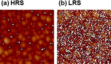
One of the most commonly observed resistive switching behaviours is the formation and annihilation of conducting filaments in resistive switching films. This filamentary switching behaviour is usually found in unipolar switching mode. The importance of the filamentary switching mechanism has become more obvious as it was recently reported that several bipolar switching behaviours are intimately related to annihilated conducting filaments.5 LC-AFM imaging has confirmed filamentary conduction in various resistive switching films including TiO2,8–10SrTiO2,11,12MoOx13 and NiO.14–16 Observations of filament formation through cation migration (metallization cell) are summarized separately in a later part.Choi et al. reported one of the earliest studies on a filamentary conducting mechanism of resistive switching films using LC-AFM in a detailed and quantitative manner.8 LC-AFM was used on a TiO2 film to probe the local conductivity of the film. Fig. 2a shows the current maps on films in a low resistance state (LRS) and high resistance state (HRS), respectively. The statistical distribution of conducting spots as a function of the local current (Fig. 2b) confirmed a denser population of high current carrying filaments in the LRS film. However, the current density extracted from the LC-AFM measurement (integration of graph area shown in Fig. 2b) far exceeded that from a pad type I–V measurement. Most of the current probably may not have travelled through the conducting filaments in the probe based measurement. Indeed, the highly nonlinear I–V behaviour, even in LRS films, through the probe (the slope is approximately four in the I–V graph in the log–log coordination) suggests that the current flow originated from a leakage mechanism, such as Schottky emission or tunnelling. Other than the possible leakage mechanisms suggested by Choi et al., this exaggerated current through the scanning probe, even on an OFF spot (out of the conducting filament region), could have originated from an electrochemical redox process during the measurement. An analytical approach based upon the local current images in both the LRS and HRS included the elimination of the current contribution from the leakage process. The insets in Fig. 2b show the resulting histograms of real conducting filaments. The analysis led to the conclusion that (1) each of the conducting spots on a LRS film has several tens of times higher conductivity than those on a HRS film, (2) the density of the conducting spots found on a LRS film also is a few tens of times higher, and (3) the change in resistance is due to the percolation of conducting filaments that gather together to form stronger and more conducting filaments during the transition to the LRS. Another interesting finding can be made from the LC-AFM scan on areas without obvious filaments in LRS and HRS samples. As shown in Fig. 2c, the average level and statistical variation of the background leakage in the LRS were higher than those in the HRS. This suggests that the metallic conducting filaments may not be the sole substance that is influenced by the subsequent switching operations, i.e., there may be other matter in the non-conducting region of a LRS film (e.g., large numbers of tiny nuclei of conducting filaments) affecting the switching/conduction behaviour.
 | ||
| Fig. 2 (a) Conductivity mapping results of TiO2 films in the LRS (upper) and HRS (lower) obtained using a reading voltage of Vtip = +1 V under high vacuum. The z-scales are 1.7 nA (upper) and 0.2 nA (lower), respectively. (b) Histogram showing the distribution of the number of conducting spots as a function of the current at each spot for the LRS (upper) and HRS (lower). ((a and b) Reprinted with permission from ref. 8.) (c) LC-AFM scan of the areas without obvious filaments in LRS (upper) and HRS (lower) films. The z-scales and root-mean-square deviation are 950 pA, 134 pA (upper) and 150 pA, 22 pA (lower), respectively. | ||
Szot et al.12 reported a similar filamentary conduction on epitaxially grown SrTiO3 films. A current map showed that the conducting spots, which are the exits of conducting filaments, have a diameter of 2–4 nm. The high lateral resolution of the current image shown in Fig. 3a may not be readily understandable considering a metal coated tip has an apex diameter of ∼20 nm. Although there has been little systematic report on the lateral resolution of current images, the high resolution shown in the figure can be attributed to (1) the formation of a tiny current path by the instantaneous breakdown of thin non-conductive contaminants between the tip and sample by the electric bias and/or (2) the fact that significant contributions to the point-contact current only come from the contact area with the highest-pressure.29,35 For a better understanding of the current transport mechanism on SrTiO3 films, the temperature dependence of the I–V curves of individual filaments was examined. The current histogram shown in Fig. 3b was drawn from numerous conducting spots in a 1 µm × 1 µm LC-AFM map. The clear temperature dependence of the conductance suggests that the filament formation process is probably a local insulator-to-metal transition due to a heat assisted redox-process. The statistical approaches, as shown in the aforementioned two reports, eliminated the unexpected irregularities/abnormalities, such as the tip–film contact area variation and thermal drift effect.
 | ||
| Fig. 3 (a) Nanoscale LC-AFM map of a 10 nm thick STO thin film under vacuum conditions and a line scan along the dashed line. (b) Exemplary current histograms extracted from the LC-AFM scans of 1 µm2STO film surface at two different temperatures—293 K and 493 K. (Reprinted with permission from ref. 12.) | ||
Another LC-AFM study on the conducting filaments in a NiO film was performed directly on ultra-thin (<5 nm) Pt films, which were also used as the top electrodes (TEs).14 Typically, a LC-AFM study is performed on a bare resistive switching film after pad-type switching processes followed by electrode removal. In the conventional procedure, the changes caused by the additional switching process cannot be observed after removing the TE. However, if ultra thin electrodes (UTEs) are used, the incremental changes in nanoscopic phenomena can be examined repeatedly after each switching process. In addition, UTEs provide much more reliable electrical contacts between the tip and film surface. A localized observation of the film beneath the conducting UTE was possible by the fact that the current through the lateral direction in the Pt UTEs is negligible under a sufficiently low voltage (<0.1 V).36 From LC-AFM observations of UTE, it is observed that (1) the localized filaments appear randomly through a forming process and (2) most of the ruptured filaments are recovered to the conducting state from subsequent set processes.14
Unlike the random distribution of conducting filaments reported in ref. 8, their restricted distribution was observed on NiO films in the pristine and HRS. This observation was made possible using a highly doped Si tip instead of a metal coated tip.15 Images using the metal coated tip cannot avoid sacrifices in lateral resolution due to the finite thickness of the metal coating for securing a reasonably high conductivity and wear-resistance. However, a doped Si tip can serve as a conducting tip with a radius as small as ∼3 nm because it has high conductivity in itself and does not require a metal coating for high conductivity. A slow scan speed (0.1 line per second) and a low tip bias (50 mV) were used for the current mapping to prevent damage to the ultra-sharp tip. Using a mercury probe system, the bulk Hg TE could be removed easily after set and reset switching. From the high resolution current image shown in Fig. 4, a leakage current was found in the HRS (even in pristine) films, but only along the grain boundaries. The highly defective grain boundary area acts as a leakage source in the HRS. However, filaments in LRS films were populated randomly without restrictive localization only at the grain boundary regions.
 | ||
| Fig. 4 LC-AFM images of a NiO film in the (a) OFF state and (b) ON state. The reading voltage was 0.1 V. The white spots correspond to conducting areas. The ON state corresponds to 100 switching cycles. (Reprinted with permission from ref. 15.) | ||
By combining a delamination technique with LC-AFM, Münstermann et al. demonstrated that the electroforming step results in the creation of localized conducting channels through oxygen evolution, and subsequent resistive switching causes additional conducting channels adjacent to the forming spot.10 The image on the right side in Fig. 5a is the current map (labelled as “C”) after electroforming with a positive bias followed by set switching with a negative bias. A comparison with a current map after only an electroforming step (data not shown) revealed the formation of conducting islands in the dashed square to be due to subsequent switching. The observation that the lateral extent of these channels shown in Fig. 5b depends on the number of switching cycles indicates an ongoing breaking of existing filaments and the creation of neighbouring ones during subsequent switching.
 | ||
| Fig. 5 Current–voltage curve, topography and LC-AFM images of (a) a sample positively formed and switched once and (b) another sample positively formed and switched several times. The dashed area indicates the conducting spots due to the switching procedures. (Reprinted with permission from ref. 10.) | ||
A new scanning probe technique, called local pressure-modulated conductance microscopy (LPCM),37 was applied to a Pt/TiO2/Pt device to show the localized conducting channel.38 The lower right inset of Fig. 6 shows a simplified experimental setup. In LPCM, unlike the conventional current-sensing techniques, bias application and current sensing are performed between the TE (not the tip) and BE. Therefore, the AFM tip is not required to be electrically conductive because it serves only to apply local pressure. This local pressure enables a locally solid electrode/oxide contact, which would otherwise be unstable or physically detached. Sometimes this pressure was also found to narrow the tunnelling gap in the locally stressed areas.39 An anodic TE bias application on a capacitor-like Pt/TiO2/Pt film was optically visualized to observe the induced oxygen gas in the same report (image not shown). The morphological protrusion formed by the oxygen gas generation was also shown in an AFM topography image (at the center of the upper image in Fig. 6). The conductance map obtained by LPCM verified that no discernible current was observed when the tip pressed down the film outside the protruded area. Even within the protruded area, only a small area was found responsible for the whole conductance in the cell. This result supports the assertion that an electroforming step creates inhomogeneous oxygen vacancies in the film, which may have resulted in highly local conducting channels.
 | ||
| Fig. 6 Conducting channel formation and dissolution adjacent to the bubble area, as observed with the local pressure-modulated conductance microscopy (LPCM). Top: a topographic image of a micron-sized device with a bubble created during the forming step. Dashed lines indicate the electrode edges. Left: LPCM conductance image of the bubble region in the low resistance state (LRS). Right: after switching back to the high resistance state (HRS) the conducting channel disappears. (Reprinted with permission from ref. 38.) | ||
Instead of observing only the exits of the conducting channels, as was mostly performed by many researchers, direct probing on the conducting filaments in a lateral configuration (combined with an in situTEM technique) was recently reported by Kwon et al.3Fig. 7a shows the setup for localized in situ current sensing on a polycrystalline TiO2 thin film in cross-section TEM. The current measured on the Magnéli filament, which was confirmed by a set of TEM results provided in the same paper, was ∼1000 times larger than that measured on a spot outside the filament (Fig. 7b). The localized conductivity measurement clearly proved that the Magnéli filament is actually the conducting path which was corroborated by the pad-type I–V measurements at low temperatures. This is one of rare reports on a local probe-based observation of conducting filaments in a lateral configuration, even though there have been several observations using other techniques, such as scanning electron microscopy (SEM),40 photo-emission electron microscopy (PEEM)41 and secondary ion mass spectroscopy (SIMS) mapping.42
 | ||
| Fig. 7 (a) Schematic diagram showing the experimental setup of in situI–V scan. (b) Local I–V curves measured on the Ti4O7 nanofilament and on the anatase structure ∼50 nm away from the filament. (Reprinted with permission from ref. 3.) | ||
Even on an undoped single crystal, bistable switching originating from oxygen transport along extended dislocations has been observed. One of the popular resistive switching materials, SrTiO3, has been found to exhibit bistable switching when doped with Cr, and the switching effect is considered a bulk property.43 However, a LC-AFM map obtained in a lateral measurement setup, where two electrodes are deposited on top of a single crystalline SrTiO3 film, clearly shows well defined high conducting filaments.11 This measurement supports the intrinsic filamentary character of conductance, even on an undoped single crystal.
A serious drawback of LC-AFM when applied to an RS cell in the metal–insulator–metal (MIM) configuration is its inability to resolve the local properties along the insulator depth direction. It is gradually becoming more evident that repeated filament formation and rupture occur at a localized vertical position along its length depending on the film type and switching procedure.44 For this reason, the capability of probing the local properties in the vertical direction with high resolution becomes very important. Unfortunately, LC-AFM has not been useful for this purpose. Alternatives to this problem (including nano-scale impedance spectroscopy) need to be further addressed.
Redox induced resistive switching
Numerous efforts have been made to reveal the switching and conducting mechanism of resistive switching memory. The analytical tools range from a variety of bulk measurement schemes to highly localized ones. Relatively bulky techniques, such as pad-type I–V measurement, impedance spectroscopy,45SEM and X-ray photoelectron spectroscopy (XPS) have been employed to determine the switching/conduction mechanism. However, by confining the lateral dimension of the target system, one can naturally exclude a significant portion of unexpected uncertainties and complexities, and simplify the problem considerably. Furthermore, combinations of a range of SPM variants, spatially resolved time-of-flight secondary ion mass spectroscopy (TOF-SIMS), TEM and other techniques with a fine spatial resolution are highly powerful for examining the mechanism.46–48 Although there are not many examples of combined local measurements for the resistive switching phenomena, a few recent observations are noteworthy.Yoshida et al.46 employed two localized measurement schemes, LC-AFM and spatially resolved TOF-SIMS, to visualize the role of oxygen in the resistive switching of p-type semiconducting NiO films. First, a sequence of biases (−7 V in 12 µm × 12 µm followed by +7 V in 4 µm × 4 µm) was applied to the back electrode (BE) while the tip was grounded in the LC-AFM setup. During the experiment, the sample was placed in an environment containing 18O gas. The LC-AFM image shown in Fig. 8a clearly revealed higher conductance in an area where a positive bias had been applied to the BE. On the other hand, TOF-SIMS elemental analysis (Fig. 8b–f) showed that 18O ions exist in the surface vicinity (down to 5 nm deep) within the positively biased region, whereas the 18O profile in the negatively biased area is similar to the unwritten region. This shows that a significant amount of oxygen incorporation into the surface actually occurred under a positive bias on the BE (a cathodic tip bias). In addition, the level of oxygen incorporation into the film surface was much more than the possible oxygen migration toward the BE. Based upon these observations, they suggested a resistive switching mechanism that the depletion or accumulation of oxygen ions at the BE interface caused by oxygen migration within the NiO film changes the conductivity of the film. However, 16O migration toward the anode (the BE in this case) within the NiO film under a +7 V bias may not have occurred significantly as they interpreted the experimental results. It is not clear whether oxygen vacancy formation actually occurred at the top surface under the anodic bias, either, considering that the O/Ni ratio at the surface remained relatively constant (or even increased slightly) under the anodic tip bias but surged from ∼0.9 to ∼1.4 under a cathodic tip bias, as shown in Fig. 8f.
 | ||
| Fig. 8 (a) Current image and (b–d) TOF-SIMS secondary ion images of the NiO/Pt film after applying a local bias. (e) TOF-SIMS depth profile of 18O ions. (f) Comparative plot of ion counts. (g) Schematic diagram of oxygen movement in HRS and LRS. (Reprinted with permission from ref. 46.) | ||
Another localized observation47 using KPM is presented to complement Yoshida et al.'s experiments. The KPM mapping on oxide films can show the local distribution of charged species, even though it cannot tell what elements they are composed of. As shown in Fig. 9b, the authors also observed the bipolar switching behaviour of NiO films using a Pt coated tip as the TE as Yoshida et al. did. Under a dc bias, approximately two scenarios on the movement of charged species can be assumed. One is that the charge transfer of ionic/electronic species through the tip/NiO interface is dominant compared to the charge transport within the NiO film (Scenario 1, Fig. 9d). For example, under a positive tip bias, (1) oxygen vacancy formation extracting oxygen ions and electrons from the NiO film and/or (2) hole injection into the film could be the dominant processes. In this case, the area applied with a positive tip bias will become effectively positive with respect to the remaining area. Hence, a KPM map on this region will show a higher value. The other scenario is when the charge transport within the NiO film is dominant (Scenario 2, Fig. 9e). Under the same positive tip bias, positively charged ionic/electronic species are repelled from the tip contact area while negatively charged species are attracted to it. The resulting KPM map would exhibit a lower surface potential in the region where the positive tip bias had been applied. An actual KPM map (Fig. 9c) showed a higher surface potential in the positively biased area, indicating that the charge transfer reaction at the interface was more dominantly reflected on the KPM image than the charge transport within the NiO film. Between the two possibilities from the KPM measurements (i.e., oxygen vacancy formation and hole injection), additional information from a LC-AFM mapping on the same area confirmed that oxygen vacancy formation (or oxygen removal) is dominant over the hole injection effect. The initially Ni-deficient composition resulted in a p-type semiconducting characteristic of the film. As oxygen atoms/ions were removed from the surface under a positive tip bias, the film became locally closer to stoichiometric NiO, making the conducting species less populated. This is consistent with the LC-AFM map showing higher resistance in the region where a positive tip bias had been applied. Hole injection (under the same positive tip bias) would produce an opposite LC-AFM result because a higher hole concentration (due to the hole injection under a positive tip bias) would incur fluent current flow. Therefore, among the many possible switching mechanisms, oxygen vacancy formation and incorporation were found to satisfy both the KPM and LC-AFM results. From ref. 35 and 36, it appears that oxygen vacancy formation and oxygen incorporation under anodic and cathodic tip biases actually occur. However, there is little proof supporting oxygen migration within the NiO film under dc biases, leaving the conclusion shown in Fig. 8g open to discussion. Furthermore, the assertion that the conductivity of a NiO film is determined by the stoichiometry in the vicinity of the BE interface is not plausible considering that a significant portion of the electric field is concentrated at the LC-AFM tip/film interface. Hence, a bottleneck for the current is more likely at that interface during the LC-AFM scan.
 | ||
| Fig. 9 (a) A simplified experimental setup for applying dc biases. An area of 2 µm × 2 µm was scanned with a tip bias of +5 V on the as-deposited NiO film (area 1), followed by another scan with −5 V over a smaller area (1 µm × 1 µm, area 2). (b) LC-AFM and (c) KPM image of the NiO film after applying bias. Two plausible scenarios that affect the LC-AFM and KPM image after scanning with dc tip biases considering (d) only the charge transfer at the surface and (e) only the charge electronic/ionic transport within the NiO film. The expected charge distribution and the resulting current and surface potential maps are depicted (ref. 47). | ||
Shima et al. examined a p-type semiconducting oxide CoO using LC-AFM, KPM and micro-XPS.48 The area where the tip had scanned with +7 V showed a higher surface potential in a subsequently obtained KPM image. A localized micro-XPS showed Co2+ peaks only in the positively biased area (anodic tip bias), indicating the partial reduction of Co–O from Co3O4 to CoO. From the KPM and micro-XPS result, it was reconfirmed that an electrochemical surface reaction (oxide reduction) actually occurred during electroforming via the tip. However, the discrepancy in the LC-AFM result between the NiO films (showing low conductance after an anodic tip bias application) and CoO is unclear at this moment. This could be due to the different majority carrier type of the two materials.
More recently, an opposite bias polarity dependence of resistive switching in n-type and p-type semiconducting oxides was presented.49 However, the conclusion was drawn mostly from the LC-AFM results. They attributed the reset process to the closeness to the stoichiometry due to the migration of oxygen ions in the films under negative and positive BE biases for the p-type and n-type oxides, respectively. However, as confirmed in the above-mentioned observations using KPM, TOF-SIMS and micro-XPS, an electrochemical reaction at the surface involving oxygen ions cannot be excluded from the switching mechanism. Indeed, the bias polarity dependence can also be interpreted only by oxygen vacancy formation and oxygen incorporation at the TE interface. For example, under an anodic tip bias, the p-type (n-type) film will be deprived of a significant amount of oxygen ions/atoms from its surface and will change to a composition closer to (or away from) stoichiometry.
Interface-dominated conduction
The LC-AFM and KPM techniques were found to be very useful, as shown above. However, if applied to a MIM structure, they cannot resolve the local distribution of the electrical quantities (e.g., resistivity, space charge, etc.) in the vertical direction nor separate the contribution of electrode/film interface to the electrical conduction from that of the film itself. ac based current measurements (impedance spectroscopy) have been used as a solution to this limitation.45,50–53 The frequency dependent current response under an ac-based voltage perturbation enables one to resolve various conduction mechanisms with distinct time constants. However, as mentioned in the Introduction section, the RC time constant formed by the stray capacitance and contact resistance limits the valid frequency bandwidth. Considering the typical stray capacitance in an AFM setup combined with conventional impedance spectroscopy ranges from 10–100 pF, the highest frequency at which reliable measurements can be made is only approximately 1–10 Hz for a resistance of 1 GΩ (Fig. 10).27 On an Ag2S/Ag nano-wire hetero-structure, the dc-bias dependent impedance spectra revealed the occurrence of charge and mass transfer at the electrode/film interface,54 but only through the micro-probe (diameter ≈ 30 µm) not scanning probe (diameter ≈ 30 nm). However, AFM based impedance spectra may be applied to systems where the localized current response is large enough to be detected, even at a reasonably high frequency. If the impedance is within the valid bandwidth range, the “reasonable frequency” is defined by the scan rate and imaging pixel per line. For example, if the scan rate and pixel per line are 1 line per second and 100 pixel per line, respectively, the allowed measurement time for a pixel is 0.01 s. In this case, at least a few hundreds of Hz as the perturbation frequency will be needed to obtain a valid impedance map. | ||
| Fig. 10 Frequency–bandwidth limitations of an AFM-based impedance measurement system. The upper bound of frequency depends on the impedance measurement or pulse generation system. The bandwidth is determined mainly by the stray capacitance in the measurement loop. (Reprinted with permission from ref. 27.) | ||
As an alternative to local impedance spectroscopy, local probe measurements in a lateral setup can be used to examine the contribution from the interface and bulk. Fig. 11 gives an example where a direct resistance profile was obtained on an electrical pulse induced resistance change device.55Fig. 11a shows the surface potential map and a line scan of the sample obtained while flowing a constant current of 1 µA through the sample between the electrodes B and C in the measurement setup. The surface potential line scan was used to generate a resistance profile, as shown in Fig. 11b. From the integrated resistance profiles of the four different switching states (data not shown), it was found that 98% of the resistance switching occurred in the interface regions within a width of approximately 1–3 µm of the electrical contact surface.
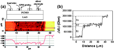 | ||
| Fig. 11 (a) Upper schematic: a simplified experimental setup for KPM imaging. Lower image: a surface potential map with a line scan obtained on the Ag–PCMO–Ag surface while flowing a 1 µA current through the two top electrodes. (b) The resulting ΔV/ΔI profile. (Reprinted with permission from ref. 55.) | ||
Resistive switching in chalcogenides
Chalcogenide film-based memory has attracted considerable interest not only as a phase change memory (PRAM)56 but also as a polarity-dependent resistance change memory.34 PRAM works by inducing an amorphous–crystalline phase transformation using electric pulses. For PRAM applications, many SPM variants, such as scanning near-field optical microscopy (SNOM) and scanning tunnelling microscopy (STM) as well as LC-AFM have been used to characterize the local phase change phenomena.57–75 Most of them focused on a parametric study of the dimension of the crystalline phase resulting from different types (optical/electric/thermal), amplitudes and duration of pulses in a range of amorphous matrices.On the other hand, polarity-dependent resistance change memory involves the movement of cations and the formation of conducting filaments in the film. In a MIM structure, cations that exist either in the film itself or in an electrode travel through the film toward the cathode under a dc bias. They accumulate at the cathode interface and eventually form filament-like (or dendrite-like) conducting channels. Under a reverse bias, the filament becomes disconnected. This electrolytic switching mechanism naturally incurs morphological changes at the cathodic interface. Only a few reports on SPM based studies in this domain have been published. Schindler et al. visualized the growth and dissolution of conductive filaments in Ag–Ge–Se films using AFM topography and LC-AFM imaging.76 In an effort to reduce the massive morphological deformation after filament formation under a cathodic tip bias, a current limiting scheme during the set process was demonstrated to confine the change in topography to a minimum.
A resistance change phenomenon on another phase changing medium, GeSb2Te4, even without morphological changes was previously reported by Kado et al.77 The bias polarity dependence of the resistive switching phenomena eliminated the possibility of a crystalline–amorphous phase change effect. No topographic deformation indicates that switching does not involve the electrolytic effect either. Consequently, they attributed resistive switching to an electronic mechanism—Schottky barrier tunnelling effect.78 Under a dc bias, charged dangling bonds generate space charges near the electrodes, and the resulting thinning/thickening of the interfacial barrier width was considered to modulate the electronic tunnelling probability.
Tip–sample interfacial effects
Schottky barrier effect
Sawa previously reported the dependence of the I–V behaviour on the Schottky barrier height at the metal–oxide interface, as shown in Fig. 12.4 In a capacitor-like metal/oxide/metal structure, where the contact between oxide and the BE was kept (quasi-) Ohmic, TEs with a higher work function on a (effectively) p-type and n-type semiconducting oxide resulted in I–V characteristics closer to Ohmic and Schottky-like behaviour, respectively (Fig. 12a).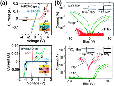 | ||
| Fig. 12 (a) I–V curves of p-type M/PCMO/SRO (upper) and n-type M/Nb:STO/Ag (lower) cells in the bulk MIM structure. M represents Ti, Au or SRO. (Reprinted with permission from ref. 4.) (b) Upper: I–V curves obtained on a NiO/Pt film using Pt and Ti coated AFM probes as the top electrodes. Lower: I–V curves on a TiO2/Ti film. Insets: a simplified conceptual band diagrams (ref. 79). | ||
The same effect applies to the contact between a scanning probe and oxide film.79 The lower graph of Fig. 12b shows the I–V curves of a TiO2(n-type)/Ti film using both a Ti and a Pt tip. The BE contact can be regarded as a quasi-Ohmic interface because the contact area of the TiO2/Ti BE is much wider than that of the tip/TiO2 contact, and thus, the TiO2/BE interface would not act as a bottleneck in the conduction loop. When a Pt tip (having a higher work function than Ti) was used, the curve shows a highly rectifying behaviour. Considering that currents lower than 10−10 A were not clearly discernible in the measurement setup, the rectification ratio is thought to be higher than 103 (under ±10 V). A positive tip bias resulted in a much larger amount of current than the opposite tip bias as expected for an n-type conductor. It is also notable that the Ti tip allowed much more current than the Pt tip. This is again consistent with the fact that (1) the work function of Pt is higher than that of Ti and (2) TiO2 is an n-type conductor. The I–V curves of a NiO/Pt film shown in the upper graph of Fig. 12b confirm the Schottky-like tip/sample contact analogously. Note that the NiO/Pt junction constitutes a quasi-Ohmic interface due to the p-type nature of NiO and high work function of Pt.
As shown in Fig. 12b, the I–V curves obtained on a NiO film and TiO2 film through a Pt and Ti coated scanning probe showed clear rectifying behaviour. In addition, the bias polarity and tip-coating dependence of conductance in the two films indicate that NiO and TiO2 films have p-type and n-type semiconducting character, respectively. The band diagrams in the insets of Fig. 12b give a qualitative explanation on the I–V behaviour.
For a quantitative measurement of the film conductivity, the Schottky barrier effect should be considered. For example, if one is interested in a quantitative assessment of the conductivity ratio between two discrete regions with different electrical properties, the ratio should not be (linearly) calculated based directly on the measured current.
Electrochemical surface reaction
During the electrical measurement in contact mode, an electric field is highly concentrated at the tip/film contact region. This is basically due largely to two reasons—(1) the tiny tip/sample contact area and (2) Schottky-like tip/film contact. Fig. 13 shows the simplified equi-potential distribution between the tip and the BE under a dc bias.79 The dense equi-potential lines, especially at the edge of tip/sample contact, indicate high electric field concentration around that area. If a metallic conductive filament (e.g., Magnéli filaments in a TiO2 film) was grown from the BE to a spot close to the tip contact through an electroforming process, the electric field concentration around the tip contact would be even more intensified.50 In the presented numerical simulation, an Ohmic tip/sample contact condition was used. Considering that the actual tip/sample contacts showing bi-stable resistive switching behaviour were always Schottky-like, the actual field intensification would be much more significant. Due to this field concentration effect, even a relatively low electric bias, which cannot induce significant electrochemical reaction in a conventional MIM structure, can cause highly localized electrochemical reaction in the vicinity of the tip/film contact. The concentrated electric field around the tip/sample interface under a positive tip bias, for example, will strongly attract negatively charged oxygen ions and reduce the film surface by forming oxygen vacancies and extracting electrons simultaneously. | ||
| Fig. 13 A finite element simulation showing potential distribution within an insulating 60 nm thick film under a +5 V dc tip bias between a scanning probe and the back electrode. An ohmic tip/sample contact was assumed (ref. 79). | ||
As detailed above, oxygen vacancy formation and oxygen incorporation obviously occur under local probe-based electric biases and most probably play a key role in resistive switching in NiO films.46,47 Similar surface redox phenomena involving oxygen ions have been observed on other resistive switching oxides.48 The aforementioned electrochemical surface reactions using a scanning probe have been shown to alter the resistance status. However, when scanning probe based techniques are used for measurement purposes, instead of surface modification, the localized electrochemical reactions can obscure the quantitative characterization of the local conduction properties.
Recently, this effect (specifically in TiO2 thin films) was reported by Shin et al.80 Self-doping by oxygen vacancies (or Ti-interstitials) generated during the deposition process resulted in an n-type semiconducting character in TiO2 films because oxygen vacancies (or Ti-interstitials) act as an effective donor in n-type TiO2. Initially, capacitor-like (Pt/40 nm thick TiO2/Pt) cells underwent switching procedures and were in the LRS. After chemical etching of the top Pt electrode, dc bias was applied through a Pt coated conducting tip on the TiO2/Pt film. When a positive tip bias was used as the reading voltage for a LC-AFM scan, the entire area showed high, almost uniform electrical conduction, as shown in Fig. 14a. However, under a negative bias, the local electrical conduction was well resolved (Fig. 14b). Here, the high conduction spots are believed to correspond to the conducting filaments. This bias polarity dependency can be attributed solely to the Schottky-like tip/surface contact characteristics. However, the time evolution of the current under positive tip biases shown in Fig. 14c suggests that the Schottky-like contact is not fully responsible for the polarity dependency. If the Schottky-like interface was the only factor, the current under the positive bias should be much higher than the current under the opposite bias at the instant the bias application was initiated (elapsed time = 0). The time scale for the transient current response (a few to a few tens of seconds) at room temperature strongly suggests the involvement of an electrochemical reaction due to the supplied electric bias. The noisy current signal under a positive tip bias was attributed tentatively to oxygen gas formation.
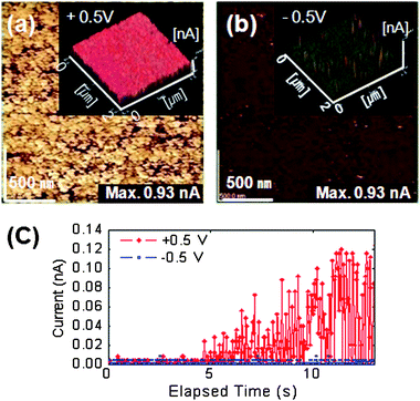 | ||
| Fig. 14 LC-AFM images using (a) Vtip = +0.5 V and (b) Vtip = −5 V obtained on a TiO2 film in the low resistance state. (c) Current–time curve using a Pt-coated AFM probe as the top electrode on a filament-free region. The noisy signal under Vtip = +5 V can be attributed to the unstable tip–surface contact caused by the formation of oxygen gas. (Reprinted with permission from ref. 80.) | ||
Although a negative tip bias would render a well-resolved conductance map compared to a positive bias, there are still chances of modifying the sample. In an oxidizing environment or even in an atmospheric environment, a negative tip bias would induce oxygen incorporation into the sample, possibly blocking the conducting channel. The number of conducting spots shown in Fig. 14b could have been much lower than the actual number of filament inlets due to partial oxygen incorporation during current imaging. To avoid this unwanted electrochemical surface reaction during current imaging, as mentioned in the Introduction part, an ac-based current measurement without (or with small) a dc bias can be considered for local conductivity observations. Measurements under high vacuum conditions can also be used to minimize the electrochemical surface reaction.
Topographical artefacts
Owing to the finite radius of the AFM probe and the resulting geometric convolution between the tip and sample surface, it is often difficult to assess the true local electrical properties when the targeted lateral resolution is comparable to or less than the tip dimension. In the case of current imaging in contact mode, the current image obtained under a constant dc bias is not uniform, even on an equi-potential surface with topographical variations (e.g., a polycrystalline Au film surface with a grain size of a few tens of nm). The resulting current map normally shows higher current around the morphological depression (along the grain boundary region), probably due to the larger tip–sample contact area at the region (data not shown). This morphological convolution issue exists not only for the current sensing techniques in contact mode81 but also for electrostatic force based techniques, such as EFM or KPM.82–84 This is because the capacitance gradient between the tip and sample surface, which intrinsically affects the signal for the electrostatic force measurement, is larger when the tip is located at a topographical depression. This effect can be circumvented using modified techniques designed for artefact suppression82 or by correcting the raw maps through modelling and simulation.83,84The use of an ultra-sharp tip would be an easier method to minimize the convolution effect in a current sensing measurement in contact mode, as observed in ref. 25. This ultra-sharp and conducting tip apex may be only possible by highly doping a Si tip because thin metal coatings with a few nanometres of sharpness would peel off easily, even with a moderate force exerted on the tip. However, it would be difficult to quantitatively measure the conductivity of a sample when a doped Si tip is used because it often becomes oxidized and forms a Schottky or MIM interface, even on well-polished metal surfaces.
Surface adsorbates
The atmospheric environment often causes additional complication to the probe based measurements because of possible physi- and chemi-sorbates either on the tip or sample surfaces. The adsorbates may block the current path85 and/or reduce the effective electric field applied to the surface.86 The existence of unwanted contamination can be indirectly checked through a current–voltage and/or a current–force sweep directly on a well polished conductive substrate (e.g., a highly oriented pyrolytic graphite).85 If the tip is blocked with an insulating layer such as oxides and insulating particles, the resulting I–V curve on a conductive substrate would not be linear. A contaminated tip would also show irregular force-dependent conductivity and/or abrupt conductance shifts at a threshold force while a tip without contamination (adsorbates) would maintain good conductivity over almost the entire force profile as long as the tip is not fully detached from the sample.A capillary condensation of liquid (presumably water) from the ambient, which is usually called a meniscus, is another type of contaminant. This liquid contamination provides the medium for an alternative current path between the tip and the sample.85,87 The resulting effective tip/sample contact area for a current-sensing measurement may then be larger than the expected/nominal area. By an electric bias, a water meniscus can be dissociated into O− and OH− oxidative ions, which then react with the sample surface. Sometimes, a water meniscus is intentionally used for nano-patterning substrates such as Si,88 GaAs89 and other metals90,91 through the local anodic oxidation process.
The effect of these contaminants is often experimentally observed as shown in the Choi et al.'s report,8 in which the total current measured in an area was much smaller and the lateral resolution was higher in high vacuum than in air. In order to avoid the contaminant effects by eliminating these unwanted adsorbates, it is necessary to expose the tip to a high temperature in a dry environment prior to measurements.29,79
Summary
SPM techniques are frequently used in RRAM studies for (1) probing conducting filaments, (2) observing redox induced resistive switching, (3) separating the bulk and interface contribution to the electric conduction, and (4) characterizing chalcogenide based resistive switching systems.As demonstrated for the identification of conducting filaments, scanning probe based techniques are useful mostly for resolving the local properties in the lateral direction. Since most of the prototypical RS devices are configured with stacks of electrode and RS layers in the vertical direction, alternatives to the conventional SPM techniques are indispensable for a further understanding of the RS behaviour. Localized impedance spectroscopy was proposed as an alternative and their limitation was also discussed.
It was found that using a range of spatially resolving techniques in combination is highly powerful in examining the switching and conduction mechanisms. Through combined observations on a few binary transition metal oxides, it became clearer that oxygen vacancy formation (and oxygen incorporation) is the crucial factor affecting the bipolar RS behaviour.
In this review, the tip–sample interfacial effects were additionally highlighted with specific focus on the Schottky barrier, electrochemical surface reaction, morphological convolution and surface adsorbate effects. The tiny tip–sample contact area and Schottky-like contact characteristic naturally result in a high contact resistance, which can induce electrochemical surface reactions even under a mild dc bias. This effect was demonstrated on a few RS films in this review. Combined with the Schottky-like contact nature, the facilitated redox reaction at the tip–sample interface can cause significant artefacts in probing the surface phenomena in a high resolution. The topographical convolution effect between the tip and sample surface is another source of measurement artefacts. Care should be taken not to be misled by these effects during nano-probing characterization.
Even though the geometry and possibly the interfacial character of the cell in a scanning probe based configuration are different from those in an MIM structure, the scanning probe based observations are still highly meaningful in terms that they enhanced the understanding and provided insight into the resistive switching phenomena. However, a systematic study on the possible discrepancy and similarity in the underlying switching/conduction mechanisms is still in need.
Acknowledgements
This study was supported by the National Research Program for the Nano Semiconductor Apparatus Development, National Research Program for 0.1Terabit NVM Devices sponsored by the Korea Ministry of Knowledge and Economy, and the Convergent Research Center program (2010K000977), and the World Class University program (R31-2008-000-10075-0) through the National Research Foundation of Korea funded by the Ministry of Education, Science and Technology.References
- R. Waser, R. Dittmann, G. Staikov and K. Szot, Adv. Mater., 2009, 21, 2632 CrossRef CAS.
- M. N. Kozicki, M. Park and M. Mitkova, IEEE Trans. Nanotechnol., 2005, 4, 331 CrossRef.
- D.-H. Kwon, K. M. Kim, J. H. Jang, J. M. Jeon, M. H. Lee, G. H. Kim, X.-S. Li, G.-S. Park, B. Lee, S. Han, M. Kim and C. S. Hwang, Nat. Nanotechnol., 2010, 5, 148 CrossRef CAS.
- A. Sawa, Mater. Today (Oxford, UK), 2008, 11, 28 CrossRef CAS.
- K. M. Kim, G. H. Kim, S. J. Song, J. Y. Seok, M. H. Lee, J. H. Yoon and C. S. Hwang, Nanotechnology, 2010, 21, 305203 CrossRef.
- J. J. Yang, M. D. Pickett, X. Li, D. A. A. Ohlberg, D. R. Stewart and R. S. Williams, Nat. Nanotechnol., 2008, 3, 429 CrossRef CAS.
- G.-S. Park, X.-S. Li, D.-C. Kim, R.-J. Jung, M.-J. Lee and S. Seo, Appl. Phys. Lett., 2007, 91, 222103 CrossRef.
- B. J. Choi, D. S. Jeong, S. K. Kim, C. Rohde, S. Choi, J. H. Oh, H. J. Kim, C. S. Hwang, K. Szot, R. Waser, B. Reichenberg and S. Tiedke, J. Appl. Phys., 2005, 98, 033715 CrossRef.
- K. M. Kim, B. J. Choi, B. W. Koo, S. Choi, D. S. Jeong and C. S. Hwang, Electrochem. Solid-State Lett., 2006, 9, G343 CrossRef CAS.
- R. Münstermann, J. J. Yang, J. P. Strachan, G. Medeiros-Ribeiro, R. Dittmann and R. Waser, Phys. Status Solidi RRL, 2010, 4, 16 Search PubMed.
- K. Szot, W. Speier, G. Bihlmayer and R. Waser, Nat. Mater., 2006, 5, 312 CrossRef CAS.
- K. Szot, R. Dittmann, W. Speier and R. Waser, Phys. Status Solidi RRL, 2007, 1, R86 Search PubMed.
- D. Lee, D.-J. Seong, I. Jo, F. Xiang, R. Dong, S. Oh and H. Hwang, Appl. Phys. Lett., 2007, 90, 122104 CrossRef.
- J.-B. Yun, S. Kim, S. Seo, M.-J. Lee, D.-C. Kim, S.-E. Ahn, Y. Park, J. Kim and H. Shin, Phys. Status Solidi RRL, 2007, 1, 280 Search PubMed.
- J. Y. Son and Y.-H. Shin, Appl. Phys. Lett., 2008, 92, 222106 CrossRef.
- I. Hwang, J. Choi, S. Hong, J.-S. Kim, I.-S. Byun, J. H. Bahng, J.-Y. Koo, S.-O. Kang and B. H. Park, Appl. Phys. Lett., 2010, 96, 053112 CrossRef.
- A. Baikalov, Y. Q. Wang, B. Shen, B. Lorenz, S. Tsui, Y. Y. Sun, Y. Y. Xue and C. W. Chu, Appl. Phys. Lett., 2003, 83, 957 CrossRef CAS.
- S. Tsui, A. Baikalov, J. Cmaidalka, Y. Y. Sun, Y. Q. Wang, Y. Y. Xue, C. W. Chu, L. Chen and A. J. Jacobson, Appl. Phys. Lett., 2004, 85, 317 CrossRef CAS.
- A. Sawa, T. Fujii, M. Kawasaki and Y. Tokura, Appl. Phys. Lett., 2004, 85, 4073 CrossRef CAS.
- T. Fujii, M. Kawasaki, A. Sawa, H. Akoh, Y. Kawazoe and Y. Tokura, Appl. Phys. Lett., 2005, 86, 012107 CrossRef.
- J. J. Yang, J. Borghetti, D. Murphy, D. R. Stewart and R. S. Williams, Adv. Mater., 2009, 21, 3754 CrossRef CAS.
- Z. Wang, P. B. Griffin, J. McVittie, S. Wong, P. C. McIntyre and Y. Nishi, IEEE Electron Device Lett., 2007, 28, 14 CrossRef CAS.
- K. Terabe, T. Hasegawa, T. Nakayama and M. Aono, Nature, 2005, 433, 47 CrossRef CAS.
- G. Binnig and H. Rohrer, Sci. Am., 1985, 253, 50 CrossRef.
- G. Binnig, C. F. Quate and C. Gerber, Phys. Rev. Lett., 1986, 56, 930 CrossRef.
- R. Berger, H.-J. Butt, M. B. Retschke and S. A. L. Weber, Macromol. Rapid Commun., 2009, 30, 1167 CrossRef CAS.
- R. O'Hayre, M. Lee and F. B. Prinz, J. Appl. Phys., 2004, 95, 8382 CrossRef CAS.
- K. M. Lang, D. A. Hite, R. W. Simmonds, R. McDermott, D. P. Pappas and J. M. Martinis, Rev. Sci. Instrum., 2004, 75, 2726 CrossRef CAS.
- M. A. Lantz, S. J. O'Shea and M. E. Welland, Rev. Sci. Instrum., 1998, 69, 1757 CrossRef CAS.
- M. A. Lantz, S. J. O'Shea and M. E. Welland, Phys. Rev. B: Condens. Matter, 1997, 56, 15345 CrossRef CAS.
- M. Nonnenmacher, M. P. O'Boyle and H. K. Wickramasinghe, Appl. Phys. Lett., 1991, 58, 2921 CrossRef.
- K. Oka, T. Yanagida, K. Nagashima, H. Tanaka and T. Kawai, J. Am. Chem. Soc., 2009, 131, 3434 CrossRef CAS.
- J. Kim, C. Ko, A. Frenzel, S. Ramanathan and J. E. Hoffman, Appl. Phys. Lett., 2010, 96, 213106 CrossRef.
- R. Waser and M. Aono, Nat. Mater., 2007, 6, 833 CrossRef CAS.
- M. Enachescu, D. Schleef, D. F. Ogletree and M. Salmeron, Phys. Rev. B: Condens. Matter Mater. Phys., 1999, 60, 16913 CrossRef CAS.
- L. L. Kazmersi and D. M. Racine, J. Appl. Phys., 1975, 46, 791 CrossRef.
- C. N. Lau, D. R. Stewart, R. S. Williams and M. Bockrath, Nano Lett., 2004, 4, 569 CrossRef CAS.
- J. J. Yang, F. Miao, M. D. Pickett, D. A. Ohlberg, D. R. Stewart, C. N. Lau and R. S. Williams, Nanotechnology, 2009, 20, 215201 CrossRef.
- F. Miao, J. J. Yang, J. P. Strachan, D. Stewart, R. S. Williams and C. N. Lau, Appl. Phys. Lett., 2009, 95, 113503 CrossRef.
- K. Fujiwara, T. Nemoto, M. J. Rozenberg, Y. Nakamura and H. Takagi, Jpn. J. Appl. Phys., 2008, 47, 6266 CrossRef CAS.
- R. Yasuhara, K. Fujiwara, K. Horiba, H. Kumigashira, M. Kotsugi, M. Oshima and H. Takagi, Appl. Phys. Lett., 2009, 95, 012110 CrossRef.
- T. Yajima, K. Fujiwara, A. Nakao, T. Kobayashi, T. Tanaka, K. Sunouchi, Y. Suzuki, M. Takeda, K. Kojima, Y. Nakamura, K. Taniguchi and H. Takagi, Jpn. J. Appl. Phys., 2010, 49, 060215 CrossRef.
- G. I. Meijer, U. Staub, M. Janousch, S. L. Johnson, B. Delley and T. Neisius, Phys. Rev. B: Condens. Matter Mater. Phys., 2005, 72, 155102 CrossRef.
- K. M. Kim, G. H. Kim, S. J. Song, J. Y. Seok, M. H. Lee, J. H. Yoon and C. S. Hwang, Nanotechnology, 2010, 21, 305203 CrossRef.
- T. Menke, P. Meuffels, R. Dittmann, K. Szot and R. Waser, J. Appl. Phys., 2009, 105, 066104 CrossRef.
- C. Yoshida, K. Kinoshita, T. Yamasaki and Y. Sugiyama, Appl. Phys. Lett., 2008, 93, 042106 CrossRef.
- M. H. Lee, S. J. Song, K. M. Kim, G. H. Kim, J. Y. Seok, J. H. Yoon and C. S. Hwang, Appl. Phys. Lett., 2010, 97, 062909 CrossRef.
- H. Shima, F. Takano, H. Muramatsu, M. Yamazaki, H. Akinaga and A. Kogure, Phys. Status Solidi RRL, 2008, 2, 99 Search PubMed.
- K. Kinoshtia, T. Okutani, H. Tanaka, T. Hinoki, K. Yazawa, K. Ohmi and S. Kishida, Appl. Phys. Lett., 2010, 96, 143505 CrossRef.
- D. S. Jeong, H. Schroeder and R. Waser, Appl. Phys. Lett., 2006, 89, 082909 CrossRef.
- Y. Xia, Z. Liu, Y. Wang, L. Shi, L. Chen, J. Yin and X. Meng, Appl. Phys. Lett., 2007, 91, 102904 CrossRef.
- T. Zhang, X. Zhang, L. Ding and W. Zhang, Nanoscale Res. Lett., 2009, 4, 1309 CrossRef CAS.
- M. H. Lee, K. M. Kim, G. H. Kim, J. Y. Seok, S. J. Song, J. H. Yoon and C. S. Hwang, Appl. Phys. Lett., 2010, 96, 152909 CrossRef.
- C. Liang, K. Terabe, T. Hasegawa and M. Aono, Nanotechnology, 2007, 18, 485202 CrossRef.
- X. Chen, N. J. Wu, J. Strozier and A. Ignatiev, Appl. Phys. Lett., 2005, 87, 233506 CrossRef.
- W. Wełnic and M. Wuttig, Mater. Today (Oxford, UK), 2008, 11, 20 CrossRef CAS.
- T. Shintani, K. Nakamura, S. Hosaka, A. Hirotsune, M. Terao, R. Imura, K. Fujita, M. Yoshida and S. Kammer, Ultramicroscopy, 1995, 61, 285 CrossRef CAS.
- S. Hosaka, T. Shintani, M. Miyamoto, A. Kikukawa, A. Hirotsune, M. Terao, M. Yoshida, K. Fujita and S. Kammer, J. Appl. Phys., 1996, 79, 8082 CrossRef CAS.
- R. Imura, T. Shintani, K. Nakamura and S. Hosaka, Microelectron. Eng., 1996, 30, 387 CrossRef CAS.
- L. Men, F. Gan, J. Sun and M. Li, Appl. Surf. Sci., 1997, 120, 171 CrossRef CAS.
- M. W. Nelson, P. G. Schroeder, R. Schlaf and B. A. Parkinson, Electrochem. Solid-State Lett., 1999, 2, 475 CrossRef CAS.
- V. Weidenhof, I. Friedrich, S. Ziegler and M. Wuttig, J. Appl. Phys., 1999, 86, 5879 CrossRef CAS.
- D. Saluel, J. Daval, B. Bechevet, C. Germain and B. Valon, J. Magn. Magn. Mater., 1999, 193, 488 CrossRef CAS.
- M. Yamaguchi, Y. Sasaki, H. Sasaki, T. Konada, A. Ebina, T. Umezawa and T. Horiguchi, Jpn. J. Appl. Phys., 2001, 40, 1578 CrossRef CAS.
- T. Gotoh, K. Sugawara and K. Tanaka, J. Non-Cryst. Solids, 2002, 299–302, 968 CrossRef CAS.
- J. Kalb, F. Spaepen and M. Wuttig, Appl. Phys. Lett., 2004, 84, 5240 CrossRef CAS.
- T. Gotoh, K. Sugawara and K. Tanaka, Jpn. J. Appl. Phys., 2004, 43, L818 CrossRef CAS.
- K. Wang, D. Wamwangi, S. Ziegler, C. Steimer, M. J. Kang, S. Y. Choi and M. Wuttig, Phys. Status Solidi A, 2004, 201, 3087 CrossRef CAS.
- S. M. Kim, M. J. Shin, D. J. Choi, K. N. Lee, S. K. Hong and Y. J. Park, Thin Solid Films, 2004, 469–470, 322 CrossRef CAS.
- O. Bichet, C. D. Wright, Y. Samson and S. Gidon, J. Appl. Phys., 2004, 95, 2360 CrossRef CAS.
- K. Sugawara, T. Gotoh and K. Tanaka, Jpn. J. Appl. Phys., 2004, 43, L676 CrossRef CAS.
- S. Gidon, O. Lemonnier, B. Rolland, O. Bichet, C. Dressler and Y. Samson, Appl. Phys. Lett., 2004, 85, 6392 CrossRef CAS.
- J. A. Kalb, C. Y. Wen, F. Spaepen, H. Dieker and M. Wuttig, J. Appl. Phys., 2005, 98, 054902 CrossRef.
- H. F. Hamann, M. O'boyle, Y. C. Martin, M. Rooks and H. K. Wickramasinghe, Nat. Mater., 2006, 5, 383 CrossRef CAS.
- S. K. Lin, I. C. Lin, S. Y. Chen, H. W. Hsu and D. P. Tsai, IEEE Trans. Magn., 2007, 43, 861 CrossRef.
- C. Schindler, K. Szot, S. Karthauser and R. Waser, Phys. Status Solidi RRL, 2008, 2, 129 Search PubMed.
- H. Kado and T. Tohda, Jpn. J. Appl. Phys., 1997, 36, 523 CrossRef CAS.
- H. Fritzsche and S. R. Ovshinsky, J. Non-Cryst. Solids, 1970, 2, 393 CrossRef CAS.
- M. H. Lee, K. M. Kim, S. J. Song, S. H. Rha, J. Y. Seok, J. S. Jung, G. H. Kim, J. H. Yoon and C. S. Hwang, Appl. Phys. A Search PubMed , in review.
- Y. C. Shin, M. H. Lee, K. M. Kim, G. H. Kim, S. J. Song, J. Y. Seok and C. S. Hwang, Phys. Status Solidi RRL, 2010, 4, 112 Search PubMed.
- R. Muenstermann, R. Dittmann, K. Szot, S. Mi, C.-L. Jia, P. Meuffels and R. Waser, Appl. Phys. Lett., 2008, 93, 023110 CrossRef.
- M. Lee, W. Lee and F. B. Prinz, Nanotechnology, 2006, 17, 3728 CrossRef CAS.
- E. Tevaarwerk, D. G. Keppel, P. Rugheimer, M. G. Lagally and M. A. Eriksson, Rev. Sci. Instrum., 2005, 76, 053707 CrossRef.
- A. Efimov and S. R. Cohen, J. Vac. Sci. Technol., A, 2000, 18, 1051 CrossRef CAS.
- S. J. O'Shea, R. M. Atta and M. E. Welland, Rev. Sci. Instrum., 1995, 66, 2508 CrossRef CAS.
- F. Peter, K. Szot, R. Waser, B. Reichenberg, S. Tiedke and J. Szade, Appl. Phys. Lett., 2004, 85, 2896 CrossRef CAS.
- N. A. Burnham, R. J. Colton and H. M. Pollock, J. Vac. Sci. Technol., A, 1991, 9, 2548 CrossRef CAS.
- R. Garcìa, M. Calleja and H. Rohrer, J. Appl. Phys., 1999, 86, 1898 CrossRef CAS.
- Y. Okada, S. Amano, M. Kawabe and J. S. Harris, J. Appl. Phys., 1998, 83, 7998 CrossRef CAS.
- H. Sugimura, T. Uchida, N. Kitamura and H. Masuhara, Appl. Phys. Lett., 1993, 63, 1288 CrossRef CAS.
- E. S. Snow, D. Park and P. M. Campbell, Appl. Phys. Lett., 1996, 69, 269 CrossRef CAS.
| This journal is © The Royal Society of Chemistry 2011 |