Structural, electronic and magnetic properties of Sn0.95Ni0.05O2 nanorods
K.
Srinivas
a,
S. Manjunath
Rao
b and
P. Venugopal
Reddy
*a
aDepartment of Physics, Osmania University, Hyderabad, India 500007. E-mail: paduruvenugopalreddy@gmail.com; Fax: +91-40-27090020; Tel: +91-40-27682287
bCentral Instruments Laboratory, University of Hyderabad, Hyderabad, India 500007
First published on 3rd December 2010
Abstract
With a view to investigate the structural, electronic and magnetic properties of Ni (5%) doped SnO2 diluted magnetic semiconductor nanorods prepared by a PEG-6000 assisted wet chemical route, a systematic investigation has been carried out. The micro structural properties were investigated by Rietveld refinement of XRD data, AFM, TEM, EDS, SAED, FTIR, Raman scattering and XPS measurements. These studies revealed that Sn0.95Ni0.05O2 nanorods have a polycrystalline single phase tetragonal rutile structure without any detectable impurity phases and the aspect ratios of the nanorods are in the range 2.85–10.2. The deconvoluted XPS core level Ni 2p spectral studies determined the oxidation state of Ni as +2. The nanosize effects and local defects are found to influence the local electronic structure of materials. From M–H, M–T, m agnetic force microscopy (MFM) and ESR studies, all the samples are found to exhibit clear room temperature ferromagnetism without any metallic clusters. The magnetization behaviour is found to depend on the overlap of percolated bound magnetic polarons and their interactions with dopant induced defects. The magnetic exchange interactions are found to depend on the aggregation behaviour of nanorods, exchange media, the surface diffusion behaviour of randomly distributed Ni ions and the modification of electronic structure.
1. Introduction
Ferromagnetism in diluted magnetic semiconductors (DMS) has been a subject of great scientific and technological interest for the past few years due to the possibility of manipulating charge and spin degrees of freedom. Recently, oxide based diluted magnetic semiconductors (ODMSs) such as Zn(TM)O and (Sn,Ti,Hf)(TM)O2 [TM: Co, Ni, Fe, Mn, etc.] were identified as an important class of functional materials and have attracted much attention of the scientific community, as they exhibit stable ferromagnetism with high Curie temperatures (TC) above room temperature.1 Apart from their potential application in high density data storage devices, magneto-optical, magnetic sensors and spintronic devices,2–5 these ODMSs are important for better understanding the insulating ferromagnetic regime to explore basic Physics and Chemistry. In addition, as ODMSs have wide band gaps, these materials are ideal for short wavelength and advanced magneto-optical applications due to the large Zeeman splitting of the electronic bands. This may be due to the possibility of exchange interactions between s, p-band electrons and d-electrons associated with the doped magnetic ions.The role of dimensionality in shaping the spin-polarized electronic structure of nanocrystalline DMSs is of particular importance to study their ferromagnetic properties. Due to peculiar structural characteristics and size effects, these materials often exhibit novel physical and chemical properties.6 Moreover, it is important to study various transport properties of one dimensional (1D) nanostructured materials due to the possibility of having quantum-size effects along two directions, and unconfined effects along the third direction. Therefore, the work on 1D nanostructured oxide based DMSs has become a new frontier of research to explore their potential applications in nanoscale spintronics, magneto-optical, high density data storage, non-volatile memory devices, nanomagnetic fluids and magnetic sensors.7–9 In fact, the exploration of novel methods for the large-scale synthesis of 1D nanostructured ODMSs is required.
Among ODMSs, SnO2 doped with transition metal ions, Co, Mn, Ni, Fe, Cr etc., has attracted considerable attention due to its transparency, unusual large sp–d exchange interactions between the magnetic ions and the band electrons, remarkable behaviour of native oxygen vacancies, high carrier density and thermal stability along with the possibility of tunable optical, surface and interface properties. Recently, Xiaofang Liu et al.10 attributed the room-temperature ferromagnetism in Zn doped SnO2 nanorods to the doping-induced interstitial defects. Recently, several authors also attributed the ferromagnetism in DMS materials to the structural or surface defects.11,12
It is important to note that with decreasing nanometric size of the materials, it is possible to increase the solubility of the dopant.13 Apart from this, suitable synthesis conditions are crucial in avoiding metallic precipitates in order to obtain room-temperature ferromagnetism without magnetic clusters. Studies on room temperature ferromagnetism in Ni doped SnO2 nanorods with improved dopant solubility are very much interesting due to higher effective mass and carrier concentration. Although there are a few studies14–17 on the origin of room temperature ferromagnetism in the nanocrystalline Ni doped SnO2 system, the results are contradictory. As far as the authors are aware, no reports on the stable room temperature ferromagnetic 1D nanostructured Ni doped SnO2 DMSs without secondary phases are available. Therefore, an effort has been made to investigate the room temperature ferromagnetism in single phase 5% Ni doped SnO2 DMS nanorods. The present investigation is also aimed at investigating the post annealing effects on various properties of these materials. For this purpose, Ni doped (5%) SnO2 nanorods were prepared by the PEG-6000 assisted wet chemical route for the first time and a systematic investigation of structural, electronic and magnetic properties has been undertaken and the results are presented here.
2. Experimental
Ni doped (5%) SnO2 nanorods were prepared by the PEG (polyethylene glycol-6000) assisted wet chemical method. In this method, high purity starting precursors of SnCl4·5H2O (0.06431617 moles) and NiCl2·6H2O (0.003385 moles) were dissolved in 100 mL doubled distilled water. The precursors were then converted into tartarates by using tartaric acid (TA) in a ratio of metal ions to TA of 1![[thin space (1/6-em)]](https://www.rsc.org/images/entities/char_2009.gif) :2. Later, 10 mL polyethylene glycol (PEG) taken from 100 g L−1 of PEG (PEG average molecular weight, 6000 g mol−1) was added to the resultant solution. Then, it was heated to ∼50 °C with continuous stirring. Later on, aqueous ammonia was added slowly by maintaining the reaction temperature at about 50 °C, until the pH reached a value between 6 and 7. The resulting gel was then dried and washed with double distilled water using a centrifuge, mainly to avoid excess PEG or chlorides or other ammonia related impurities, if any. Subsequently, the precursor was calcined at 250 °C for 6 h and finally annealed at different temperatures between 350–650 °C for 3 h in air. During the preparation of the samples, immense care was taken to avoid contamination of magnetic impurities through accidental or trace impurities. In this process, PEG acts as morphology-director and prevents the formation of Sn and Ni clusters during the gelation process. Further, tartaric acid was used to convert the amorphous fraction to the crystalline rutile structure at relatively low temperatures.
:2. Later, 10 mL polyethylene glycol (PEG) taken from 100 g L−1 of PEG (PEG average molecular weight, 6000 g mol−1) was added to the resultant solution. Then, it was heated to ∼50 °C with continuous stirring. Later on, aqueous ammonia was added slowly by maintaining the reaction temperature at about 50 °C, until the pH reached a value between 6 and 7. The resulting gel was then dried and washed with double distilled water using a centrifuge, mainly to avoid excess PEG or chlorides or other ammonia related impurities, if any. Subsequently, the precursor was calcined at 250 °C for 6 h and finally annealed at different temperatures between 350–650 °C for 3 h in air. During the preparation of the samples, immense care was taken to avoid contamination of magnetic impurities through accidental or trace impurities. In this process, PEG acts as morphology-director and prevents the formation of Sn and Ni clusters during the gelation process. Further, tartaric acid was used to convert the amorphous fraction to the crystalline rutile structure at relatively low temperatures.
Thermogravimetric and differential thermal analyses have been carried out using a Shimadzu Thermal Analysis System model DTG–60H. The XRD patterns were recorded using a Phillips (X'pert) diffractometer with Cu Kα radiation (λ = 1.5406 A°) in the range of 20–80°. The detection limit of the X-ray diffractometer employed was ∼1.5%, which is below the doped concentration (5%) of nickel. X-Ray patterns were analyzed by the MAUD (Materials Analysis Using Diffraction) program.18 The instrumental broadening, such as instrumental asymmetry and Gaussianity of reflections, were estimated using a Si standard sample. Atomic force microscopy studies were undertaken with a CP-II, Veeco Instruments by using phosphorus (n) doped Si probes (Model: RTESPA-CP, MPP-11123) in tapping mode. Transmission electron microscopy (TEM) studies were undertaken using a JEOL JEM-200CX at 160 kV. The elemental analysis has been carried out by EDS attached to TEM and X-ray photoelectron spectroscopy (XPS) [Model: KRATOS AXIS165]. The error in the elemental analysis of EDS data is found to be 1.2% and in the analysis of surface composition of XPS data is found to be 0.6% Fourier transform infrared (FTIR) spectra of the powders were recorded using an AVATAR330 FTIR thermo nicolet spectrometer in the range of 4000–400 cm−1. The Raman spectra were studied at room temperature by using a WiTec GmbH confocal micro Raman equipped with a CCD detector. The light source was a Nd:YAG laser of 532 nm wavelength. The background and the Rayleigh line corrections have been made by using a commercial high purity (99.99%) SnO2 powder. The spectral resolution is 1 cm−1. To study the electronic state of elements and also to understand the electronic structure of the materials, X-ray photoelectron spectroscopic (XPS) measurements were performed on a KRATOS AXIS165 X-ray photoelectron spectrometer. Using an excitation energy of 1253.6 eV (Mg Kα), the spectra were recorded with pass energy of 80 eV. The angle between the detector and the X-ray flux direction was constant and equal to 90°, while the measurements were made at an electron take off angle of 70°. The calibration of the spectrometer was done using C1s (at 285 eV) features. After removing some of the surface material by Ar+ sputtering, total survey scans were performed. In order to account for the binding energy values and to minimize the surface charge contributions, the binding energies were corrected for the charging effect with reference to the peak position of Sn 3d5/2 at 486.7 eV. The maximum error in these measurements may be ±0.01 eV. In order to estimate the optical band gap values, the optical absorbance measurements were undertaken at room temperature using a UV-visible spectrophotometer (Model: Evolution 300, Thermo electron corporation) in the wavelength range 200 to 600 nm by dispersing the powders in absolute methanol solution. To make the base line corrections for the band gap values due to free excitons near the band gap, the absorbance spectra of all samples were corrected using the undoped SnO2 as a reference. The photoluminescence studies were carried out to study the behaviour of oxygen vacancies using a fluorolog spectrofluorometer (Jyobin Vyon) with a 450 W xenon lamp source. Magnetization versus applied magnetic field (M–H) measurements at room temperature up to 15 kOe and magnetization versus temperature (M–T) measurements in the temperature range 80–300 K at a constant applied field 500 Oe were undertaken using Vibrating Sample Magnetometer (Model: DMSADE 1660 MRS). Electron spin resonance spectra were also recorded at room temperature on a JOEL PE-3X X-band spectrometer equipped with a 9153.593 MHz field modulation unit. All ESR measurements were carried out by using DPPH (g = 2.00455) as a standard. The error in evaluating geff is ≈ ± 0.02. Magnetic force microscopy (MFM) images were recorded in the MFM mode of an atomic force microscope (AFM model CP-II Veeco Instruments) using a commercial CoCr coated SiN probe (model: MESP). For all the MFM measurements, air damping effects are meticulously avoided by the high vacuum setup. The MFM probe was magnetized using a commercial MFM tool kit (Model: PSIT-0005 for CP-II SPM).
3. Results and discussions
The thermal decomposition behaviour of the calcined precursor was analysed from TGA/DTA plot shown in Fig. 1. The loss of weight was monitored by heating the material at a rate of 10 °C min−1 in air up to 1000 °C. It can be seen from the figure that the decomposition step is initiated around 240 °C and ends up to around 400 °C. The peak onset from DTA plot was found to be ∼330 °C. This temperature may be attributed to the starting crystallization temperature of the tetragonal rutile phase. The associated weight loss may be due to the removal of crystallizing water, organic matrix and the residual carbon during the combustion of the precursor material. As expected, the decomposition reaction is strongly exothermic which is evident from the DTA plot (shown in Fig. 1). The weight change in the step region is approximately 23.5% and the enthalpy change is 381 J g−1. Further, the weight loss in the temperature range 400–700 °C may be attributed to the removal of the remaining crystallizing water or O– H bonds associated with the metal ions. It may be concluded from this thermal analysis that the crystallization process of the material improved at a temperature of about ∼330 °C. Therefore, post annealing was carried out in air between 350–650 °C to vary the aspect ratio of the samples.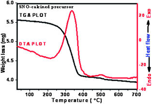 | ||
| Fig. 1 Thermogravimetric and differential thermal analysis plot of Sn0.95Ni0.05O2 calcined powder. | ||
The Rietveld refined XRD patterns (in the logarithmic intensity scale) of Ni doped (5%) SnO2, annealed at different temperatures, are shown in Fig. 2. The diffraction peaks are indexed to the tetragonal rutile structure of SnO2 and are in good agreement with the JCPDS data of SnO2 (JCPDS 41-1445). A careful phase analysis (at logarithmic scale) has been carried out using the Rietveld technique. From the Rietveld refined patterns, Fig. 2, it has been found that the Bragg peaks (red vertical bar lines) corresponding to Ni2O3, Ni, SnO and NiO phases are not matched even to the logarithmic scale intensity. However, Bragg peaks corresponding to the SnO2 phase are found to match well with the XRD patterns. Therefore, it has been concluded that Ni ions are substituted in the host lattice without any detectable impurity phases. The computed cell parameters and the rms micro strain values are given in Table 1. Further, these lattice parameters are comparable with those of undoped micro crystalline SnO219 indicating clear formation of solid solutions. From the table it has been found that both the cell parameters ‘a’ and ‘c’ are found to decrease gradually with decreasing annealing temperature. This slight shrinkage may be attributed to the variation of rms strain influenced by local structure and nanoscale effects in the octahedral co-ordination of the rutile structure. In fact, the modification of the surface condition of nano-grains and the surface to volume ratio by changing the annealing temperature results in enhancement of the surface tension. This is responsible for the origins of the rms strain in the nano-grains and thereby effecting the lattice dilatation. It can be seen from Table 1 that ‘c/a’ (lattice distortion) values are found to increase with decreasing rms strain values and the observed behaviour may be attributed to the relaxation of internal residual tensile stress/strain originated during the growth of nano-grains and surface diffusion of randomly distributed Ni ions. Further, the nanometric size and annealing temperature might have influenced the distribution of local defects. Therefore, the local disorder is crucial in understanding the structure–property relations. The surface topography images were recorded using an atomic force microscope (AFM) in a tapping mode on the surfaces of uniaxially palletized samples annealed at different temperatures. From AFM topography studies, an array of aggregated nanorod-like morphologies has been observed in all the samples. A typical AFM 2D topography image of the SNO-500 sample is shown in Fig. 3(a). From various line profile measurements of individual nanorods on different samples, the average aspect ratio is found to increase from ∼2.85 to 10.21 (Table 1) with increasing annealing temperature. In addition to AFM topography studies, TEM studies were also performed on dispersed powder samples and confirmed the formation of the nanorod-like morphology and their aspect ratios are as given in Table 1. In the samples of the present investigation, the average lengths of the nanorods are found to increase from ∼25 to 230 nm with increasing annealing temperature, while their average widths increase from ∼10 to 30 nm. A typical TEM morphology image of SNO-500 sample is shown in Fig. 3(b) along with its EDS spectra shown in the inset, whereas the inset image in Fig. 3(c) shows a single nanorod AFM image. With a view to understand the secondary phases, if any, at the nanoscale, a systematic investigation of selected area electron diffraction patterns (SAED) has been carried out. After careful analysis of these patterns, it has been confirmed that Ni (5%) doped SnO2 nanorods have a tetragonal rutile structure without any diffraction spots or rings related to secondary phases. Fig. 3(d) represents a typical SAED pattern of the SNO-500 sample. These results are in good agreement with those of the Rietveld refined (at logarithmic scale) XRD phase analysis. Further, the analysis of TEM images revealed that the nanorods of the present investigation might have grown at the expense of the small particles with increasing annealing temperature and that the nanorods might have aggregated leading to local defects.
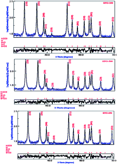 | ||
| Fig. 2 Rietveld refined XRD patterns of Ni (5%) doped SnO2, annealed at different temperatures. | ||
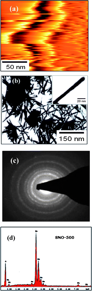 | ||
| Fig. 3 A typical (a) AFM topography image, (b) TEM morphology image, (c) typical TEM image of single nanorod image, (d) electron diffraction pattern and (e) EDS spectra of the SNO-500 sample. | ||
| Sample code | SNO-350 | SNO-500 | SNO-650 | |
|---|---|---|---|---|
| Annealing T/°C | 350 | 500 | 650 | |
| Rietveld refined XRD data | <a>/Å | 4.735 | 4.739 | 4.744 |
| <c>/Å | 3.184 | 3.189 | 3.194 | |
| (c/a) | 0.67254 | 0.67277 | 0.67327 | |
| rms micro strain | 0.001267 | 0.001220 | 0.001179 | |
| Rw (%) | 6.79 | 7.97 | 7.41 | |
| Rexp (%) | 4.76 | 5.46 | 5.68 | |
| Rb (%) | 7.20 | 7.03 | 6.49 | |
| Aspect Ratio | From AFM | 2.85 | 6.78 | 10.21 |
| From TEM | 3.02 | 6.95 | 10.2 | |
Although, Chun-Ming et al.16 reported the formation of Sn1−xNixO2 nanorods at lower Ni content (below x = 3%), the authors failed to obtain nanorods at higher Ni concentrations (x = 5 and 25%). In fact, due to the complex chemistry involved in the preparation, the resulting properties depend on the synthesis conditions and the preparation technique. Moreover, these also influence the structural and surface defects. Thus, it is clear that controllable synthesis conditions are crucial to activate the room temperature ferromagnetism. Therefore, the authors of the present investigation implemented a simple method of PEG-6000 assisted wet chemical route to overcome the synthesis of ferromagnetic Ni doped (5%) SnO2 nanorods. Earlier, the growth of 1D nanostructures20 using the PEG-6000 polymer was reported. In the present investigation, the growth mechanism and chemical process involved in the nanorod formation may be explained as follows: initially stoichiometric quantities of SnCl4 and NiCl2 were converted to its metal tartarates. Here the addition of PEG helps to separate Sn1−xNix tartarates due to the long chains of polymer. The gel grown after the addition of ammonium hydroxide mainly consists of Sn1−xNix(OH)y, Sn1−xNix tartarate and solidified PEG of different chain lengths. When the washed precursor is calcined (at 250 °C or above), the hydroxides and tartarates of Sn1−xNi1−x decompose to form SnO6 octahedra on the surface of PEG polymer matrix. The adsorption of PEG might have led to the growth of the nanorods along a certain direction. During the formation of SnO2:Ni nanorods, PEG acts as a soft template, resulting in one dimensional growth of the grain. It is well known that PEG plays an important role in determining the morphology of SnO2.21 Here, PEG is an agent that causes heterogeneous nucleation, due to its lower activation at the polymer/water interface, and helps in the growth of Sn1−xNixO2−x nanorods. Although a variety of other factors, such as van der Waals, hydrogen bonding, and hydrophobic forces, play important roles in forming a stable complex, it mainly depends on the type and length of the morphology director, degree of substitution and is also affected by the solubilization effect of Ni doped SnO2 nanorods. Moreover, the surface charge on the molecule also helps in pairing ions with the cationic molecules.
The atomic percentage values (at%) of Sn, Ni and O elements of all the samples estimated from the energy dispersive spectroscopy (EDS) studies from TEM and X-ray photoelectron spectroscopy studies are listed in Table 2. It can be seen from the table that the at% of Ni dopant is close to nominal stoichiometry. In the case of oxygen content, a slight deficiency was observed in all the samples. However, with increasing annealing temperatures slight fluctuations are found in the oxygen stoichiometry. This might be due to the charge imbalance caused by Ni substitution or redistributions of local defects with varying aspect ratio and annealing temperature of the nanorods, indicating a clear influence of the surface condition of nano-grains. Moreover, the surface condition of the nano-grains and their morphology might have also been responsible for the rearrangement of surface atoms and migration of surface defects, or oxygen vacancies, thereby changing the surface stoichiometry. Thus, these studies suggest that the stoichiometry and oxygen vacancies of the samples of the present investigation may be controlled by tuning the annealing temperature, nanometric size of the grains and their surface morphology.
In order to understand the effects of surface modification and removal of impurities on the local disorder of the materials, FTIR studies were undertaken. Fig. 4 shows the FTIR spectra of all the samples of the present investigation. The peak at ∼ <800 cm−1 is attributed to the SnO2 phase. A broad band appeared at ∼675 cm−1 due to the O–Sn–O lattice mode, while that at ∼613 cm−1 is assigned to the antisymmetric Sn–O–Sn stretching mode of the surface-bridging oxide formed by condensation of adjacent surface hydroxyl groups. The peak at ∼550 cm−1 manifests the lattice imperfections in the large size of nanometric grains of the samples. Two asymmetric peaks observed at ∼666 and ∼468 cm−1, associated with Sn–O–Sn stretching modes are in agreement with those of pristine nanocrystalline SnO2.22 Interestingly, with increasing annealing temperature, the width of the Sn–O–Sn band decreases while that of O–Sn–O band is increases. This behaviour may be attributed to the improvement in crystallinity due to the removal of residual organic impurities or crystallized water and compensation of oxygen stoichiometry. The bands that appeared in all the samples at around 1657 cm−1 may be attributed to the bending mode of O–H bonds. The broad band that appeared in the region 3000–3700 cm−1 might be assigned to the vibration of adsorbed water and is found to decrease gradually with increasing annealing temperature. This indicates that de-hydrolysis of the samples is crucial in modifying the surface and local nanostructure and morphology by the gradual strengthening of bondings associated with the local vibrational modes of metal ions. These results are in agreement with those of the FTIR results of pristine SnO2 nanorods.23 Thus, the changes observed in their shapes, widths and peak positions in FTIR spectra of all the samples with varying annealing temperature may be attributed to the variation in the local defects, grain size and shape of Ni doped SnO2 nanorods and their distributions.
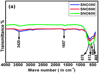 | ||
| Fig. 4 FTIR spectra and of Ni doped (5%) SnO2 nanorods annealed at different temperatures. | ||
Raman spectroscopy is a non-destructive technique and is extensively used to study the substitution of dopants in the host lattice, to analyze the impurity phases and to understand the vibrational modes. In the present investigation, Raman scattering studies were mainly focused on understanding the influence of nanometric size, surface modification, dopant distribution effects and local disorder effects on vibrational modes. The Raman spectra of Ni (5%) doped SnO2 nanorods annealed at different temperatures is shown in Fig. 5. Three fundamental Raman modes of Ni doped (5%) SnO2 nano-rods, viz. Eg at ∼472–474 cm−1, A1g at ∼619–632 cm−1, and B2g at ∼768–774 cm−1, are similar to those of tetragonal rutile undoped SnO2 nanorods,24 confirming the absence of impurity phases. This observation is consistent with the XRD results. Moreover, the intensity of peaks drastically decreased with respect to undoped bulk rutile SnO225 indicating the substitution of Ni2+ ions in the SnO2 host lattice. The three fundamental Raman peaks are found to broaden and shift with respect to bulk SnO2.25 It is also interesting to note that these modes shift towards the lower wavenumber side and that their shapes get progressively broader with decreasing nanometric size of the materials. This may be due to the influence of aspect ratio of the nanorods and the induced internal strain effects. Further, a continuous enhancement of FWHM of the Raman peaks with decreasing aspect ratio may be due to the phonon confinement effect. According to the phonon confinement model26 the long-range order and the full translational symmetry might have changed due to the size confinement effect of nanorods, resulting in the variation of the lattice vibration mode. Further, as the surface properties are sensitive to the oxygen vacancies and their distributions associated with the grain's structure and the local disorder at nanoscale dimensions, there may be a possibility for new modes appearing in the Raman spectra.
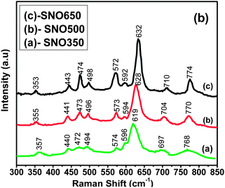 | ||
| Fig. 5 Micro-Raman spectra of Ni doped (5%) SnO2 nanorods annealed at different temperatures. | ||
New Raman peaks may also be possible when the size of SnO2:Ni nanorods is reduced to lower dimensions due to the activation of disorder. In the present investigation, in addition to the three fundamental peaks, new Raman peaks have been observed. The peaks at ∼440–443, 494–498, and ∼698–711 cm−1 may be due to the presence of local surface disorder of the nanorods.27,28 The peaks around ∼357–353, ∼574–572, and 596–592 cm−1 are attributed to the surface phonon modes and are found to shift gradually to the lower wavenumber side with increasing nanometric size and annealing temperature and may be due to a variation in the large surface area of the small sized nanorods. Moreover, these peaks are also in agreement with those obtained by using the Matossi force constant model.29 The two peaks around ∼357–353 and ∼574–572 cm−1 are also observed in nanorods of undoped SnO2.30 The observed shift of the peaks may be attributed to the non-homogenous small dispersion in the large surface area of small sized nanorods along with the activation of lattice disorder.
In order to determine the electronic state of the elements, substitution and the elemental surface composition of Ni cations in SnO2 nanorods, XPS studies were undertaken. From the total survey scans of all the samples, the core level XPS spectra of the constituents of Sn 3p, Ni 2p and O1s were deconvoluted and analyzed using a non-linear least squares curve fitting program (XPSPEAK4.1 software) with an asymmetric Gaussian–Lorentzian sum function and Shirley background subtraction. The XPS core level Ni 2p spectrum is as shown in Fig. 6(A) and the Gaussian fitted results of core level Ni 2p and O1s XPS peaks are given in Table 3. The error percentage of the binding energy (BE) values is around ± 0.10 eV. The satellite peaks of Ni 2p3/2 and Ni 2p1/2 core levels are clearly observed and represented as S1 and S2 in both Fig. 6(A) and Table 3. These results are in agreement with those of earlier ones.17,31,32 From these results, it has been found that Ni 2p3/2 positions are quite different from those of metallic Ni (∼852.3 eV), NiO (∼853.4 eV) and Ni2O3 (∼856.7 eV).32,33 The absence of NiO may be analyzed further by other features of the energy difference between Ni 2p3/2 and Ni 2p1/2 peaks and this value is in the range of 17.308–17.850 eV (Table 3) which is less than that for NiO (18.4 eV).33,34 The above results strongly suggest that Ni ions successfully substituted in the tetragonal rutile SnO2 lattice without forming any detectable impurity phase such as Ni, Ni2O3, or NiO. Therefore, it is considered that Ni ions dissolved in the SnO2 matrix and substituted at the Sn site.
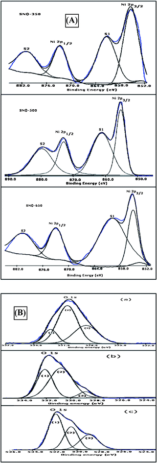 | ||
| Fig. 6 XPS core level deconvoluted (A) Ni 2p spectra and (B) O 1s spectra of a) SNO-350, b) SNO-500 and c) SNO-650 samples. | ||
| Samples | SNO-350 | SNO-500 | SNO-650 | |
|---|---|---|---|---|
| BE (eV) | Ni 2p3/2 | 855.387 | 855.252 | 855.127 |
| Ni 2p1/2 | 872.695 | 872.949 | 872.978 | |
| ΔBE between Ni 2p3/2 and Ni2p1/2 | 17.308 | 17.851 | 17.697 | |
| Satellite Peaks | S1 | 861.072 | 860.344 | 859.989 |
| S2 | 880.889 | 880.742 | 880.540 | |
| FWHAM/eV | Ni 2p3/2 | 4.369 | 3.410 | 2.872 |
| Ni 2p1/2 | 3.905 | 4.236 | 3.872 | |
| Area | Ni 2p3/2 | 38810.36 | 48110.16 | 8482.60 |
| Ni 2p1/2 | 32129.86 | 41053.17 | 37170.25 | |
| BE of O1s/eV | Peak(1) | 532.259 | 532. 104 | 531.890 |
| Peak(2) | 530.369 | 530.784 | 530.520 | |
| Peak(3) | 528.358 | 528.784 | 528.90 | |
| FWHAM of O1s/eV | Peak(1) | 1.67 | 1.51 | 1.48 |
| Peak(2) | 2.54 | 2.26 | 1.57 | |
| Peak(3) | 3.01 | 1.43 | 1.83 | |
| Optical energy band gap Eg/eV | 3.223 | 3.306 | 3.395 | |
It is well known that the peak positions depend on the local structure of Ni atoms and provide information on the chemical state. Therefore, the oxidation states of Ni were examined from the XPS Ni 2p core level spectra (shown in Fig. 6(A)). In the present investigation, the positions of Ni 2p3/2 and Ni 2p1/2 are found to be in the range ∼855.35–855.12 eV and ∼872.695–872.978 eV, respectively. These Ni 2p3/2 peak positions are quite different from those of metallic Ni, and Ni2O3 and close to the value of NiO, for which the binding energies from 854.5 to 854.9 eV are assigned.31,33 Earlier, the characteristics of divalent nickel Ni(II) was confirmed based on the peak positions of Ni 2p3/2 (in the range of ∼853.3–854.4 eV) and the shake-up satellite peak (at ∼860.1 eV).33 However, in the samples of the present investigation, Ni 2p3/2 and 2p 1/2 peak positions are found to exhibit a positive shift compared to the metallic nickel (853.0 eV),33 and NiO (∼854.5 to 854.9 eV).31,33 This might be due to more positively charged surface Ni2+.35 Therefore, from the core level Ni 2p3/2 peak positions along with their corresponding satellite structures, it has been concluded that the oxidation state of Ni is +2 and the annealing process does not influence the chemical state of the nickel in all the samples. It has been found from Table 3, that BE values of core level Ni 2p3/2 peak are found to decrease, whereas BE values of core level Ni 2p1/2 peak are increasing systematically with increasing annealing temperature and nanometric size of Ni (5%) doped SnO2 nanorods. The local charge imbalance created by random distribution of Ni2+ ions might have resulted in the formation of local or surface defects such as oxygen vacancies. Therefore, the variation in binding energy values of core level Ni 2p is dependent on the number of oxygen vacancies. This may be attributed to a change of the Fermi level position in the semiconductor gap or band bending or both. Moreover, oxygen vacancies near the surface act as n-type donors. Therefore, the band gap states are localized below the bottom of the conduction band and whose occupancy significantly affects the Fermi level position in the gap. In general, as the stoichiometric surface does not possess any filled electronic states in the band gap, the Fermi level is expected to be closer to the valence band, and vice versa. However, in the present investigation, the Fermi energy level is expected to move towards the conduction band with increasing oxygen vacancies and the Fermi level may be closer to the conduction band. From the XPS results it has been found that the core level energy difference between Ni 2p3/2 and Ni 2p1/2 peaks is found to increase systematically from 17.308 to 17.850 eV with increasing annealing temperature and nanometric size, indicating a clear influence of nanometric size on the spin–orbital splitting of Ni2+ ions in the lattice. The analysis of core level Sn 3d5/2 and Sn 3d3/2 binding energy values revealed that the oxidation state of Sn is +4 and is not found to vary with varying annealing temperature and nanometric size of the samples. Moreover, the observed spin–orbit splitting values of Sn (3d) were found to be in the range ∼8.4–8.6 eV. Further, the FWHM of the core Sn (3d) level spectra also does not indicate any variation.
With a view to study the behaviour of oxygen vacancies, deconvoluted core level XPS O1s spectra were also analyzed. The O1s spectrum (Fig. 5(B)) shows that multi-component oxygen species are present in the sample. The typical Gaussian fitted O1s peak positions are found to exhibit three components and their BE are given in the table. From these results, the peak (1) around ∼531.5–532.7 eV may be attributed to O22−, O− and OH− ions in the oxygen deficient regions,36 whereas the peak (2) around ∼530–531 eV may be due to the related lattice oxygen, O–Sn–O bonds, and O2− ions.36 Finally, the peak (3) in the range ∼528–529 eV might be attributed to O2− ions adsorbed on the surface37 of SnO2:Ni nanorods. It can be seen from Fig. 6(B) that the intensity and FWHM, after an initial decrease, are found to increase. This may be due to induced effects of inter/surface diffusion behaviour of Ni2+ ions with varying annealing temperature. All these results are in conformity with those of XRD and EDS.
It is well known that doping of magnetic ions and their nanometric size affects the optical properties of a semiconductor significantly. When a divalent 3d impurity ion, such as Ni2+, substituted for a tetravalent Sn4+ ion in SnO2, it causes an axial distortion due to s, p–d hybridization and charge imbalance. This in turn influences the strong coulomb interactions between 3d electrons located near the optical band gap region. Therefore, with a view to understand the local electronic structure and to study the annealing effects on the optical properties, UV–vis absorbance measurements were undertaken. The optical absorption coefficient (α) has been calculated form the optical absorption spectra using the relation
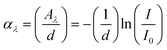 | (1) |
| α = (Ah−1ν){hν − Eg}m | (2) |
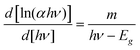
| ln (αhν) = ln A + mln (hν − Eg) | (3) |
 | (4) |
Eqn (4) indicates that a plot of d[ln(αhν)]/d[hν] versus hν exhibits a divergence at hν = Eg from which we can obtain a rough estimate of Eg. Now by using eqn (3), the value of ‘m’ may be evaluated from the slope of the plot of ln (αhν) versus ln (hν − Eg). The value of ‘m’ is in the range of 0.51–0.53, indicating the direct allowed band. Therefore, using m = 1/2, the effective band gap values of the direct allowed transition were determined from the plots of (αhν)2versus hν by extrapolating the linear region to zero absorption (baseline corrections have eliminated the free carrier contributions for determining optical band gaps). Fig. 7(A) shows the band gap energy plot. The computed band gap values are given in Table 3 and are found to be in agreement with the reported ones.16,17 The decrease of band gap values with respect to undoped SnO2 (∼3.56 eV), is a clear indication of incorporation of Ni2+ into SnO2 lattice and may be attributed to the induced band gap renormalization effect39 and originates from the band gap shrinkage and free carrier screening effects. It is interesting to note that with decreasing aspect ratio, the band gap values are found to decrease gradually, indicating a clear red shift and may be attributed to the strain induced effects. The variation of the band gap values indicates a clear modification of local electronic structure. The s, p–d hybridization, and local disorder combinedly lead to changes in the local electronic structure of the materials. Moreover, the strain in the nanorods might have also affected the optical properties, resulting in the change in the local electronic structure of the materials. In principle, the strain would tend to be higher in smaller sized nanorods, as the strain energy increases with volume prompting the larger rods to relax.
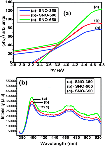 | ||
| Fig. 7 (a) Optical band gap plot and (b) PL emission spectra of Ni (5%) doped SnO2 nanorods annealed at different temperatures. | ||
Photoluminescence studies are important to investigate the structural defects, such as oxygen vacancies. In the present investigation, the emission spectra were recorded at excitation wavelengths (λex) of 385 (3.22 eV), 375 (3.30 eV) and 365 nm (3.39 eV) for SNO-350, SNO-500 and SNO-650 samples, respectively, and are as shown in Fig. 7(B). All the samples are found to exhibit a strong UV emission at ∼396 nm (3.13 eV) and a weak broad blue emission peak at ∼471 nm (2.63 eV). The peak around ∼396 nm (3.13 eV) is assigned to the direct recombination of conduction electrons in the Sn 4p band and a hole in the O 2p valence band. In the present investigation, a new peak was also detected in the PL emission spectra at ∼516 nm and is assigned to the oxygen vacancy which is in agreement with an earlier report.40 The intensity of the emission peaks are found to decrease with increasing annealing temperature and the behaviour may be due to decreasing oxygen vacancies. Further, it is interesting to note that the intensity of the emission spectra of Ni (5%) doped SnO2 nanorods is found be high. This might be due to the influence of aspect ratio on the electronic structure of nanorods along with Ni dopant and defects in the host thereby effecting the strong mixing of charge transfer states, resulting in the enhanced luminescence in the nanorods. From these studies, it has been concluded that the oxygen vacancies and their distribution not only depend on annealing temperature and random distribution of Ni ions but also on the surface condition of nanograins.
M–H hysteresis curves of all the samples are shown in Fig. 8 (a, b, c) and their corresponding inset images show their remanence and coercivity images up to a maximum of 15 kOe field. It is interesting to note that all the samples of the present investigation are found to exhibit clear room temperature ferromagnetism. Earlier, the room temperature ferromagnetism was reported in Sn1−xNixO2 nanopowders.15,17 Interestingly, in the present investigation, the room temperature ferromagnetism has been observed in the case of nickel (5%) doped SnO2 nanorods with higher magnetic moments. The specific magnetization, coercivity and remanence values along with aspect ratio are given in Table 4. In spite of the maximum spin-only saturation moment of Ni2+ being 2.0 μB/Ni2+, the maximum magnetic moment obtained in the present investigation is 0.925 μB/Ni2+ for 5% Ni doped SnO2 nanorods annealed at 500 °C, and is in agreement with the reported one.15 This high value of Ms (0.925 μB/Ni at 300 K) may not be from Ni metal clusters, as Ms of Ni metal is 0.6 μB/Ni.41Fig. 8(d) shows the temperature-dependent magnetization M(T) of field cooled Sn0.95Ni0.05O2 nanorods at 500 Oe. With increasing temperature the magnetization values are found to decrease, which may be due to thermal vibrations becoming strong enough to overcome the Zeeman interactions and initiate randomization of the magnetic moments. Further, it has been concluded that the Curie temperatures of the samples of the present investigations might be above 300 K. The curve obtained in a magnetic field of 500 Oe shows a non-zero magnetization up to room temperature, which is in accordance with the behaviour exhibited by the M–H curves. Further, the M–T behaviour of the present samples confirms the characteristic feature of nanostructured materials. From the M–T plots, the net magnetization is found to increase gradually with increasing annealing temperature. It was reported earlier that nanocrystalline NiO exhibits weak ferromagnetism (Tc < 5 K)42 or super paramagnetic behaviour at low temperatures.43,44 Similarly, it is also known that microcrystalline NiO is an antiferromagnetic material with a Neel temperature of 520 K.45 However, the synthesis of the DMS nanocrystals was performed under oxidizing conditions in which metallic nickel is unable to form. Moreover, it has been confirmed from XPS core level Ni 2p spectra that these metallic fcc nickel precipitants may not be present. In fact, as indicated by XRD, EDS, FTIR, Raman scattering and XPS results, the presence of secondary phases, including Ni clusters and NiO phases, may be ruled out. Therefore, one may conclude that the observed ferromagnetism might have originated from the Sn1−xNixO2 phase.
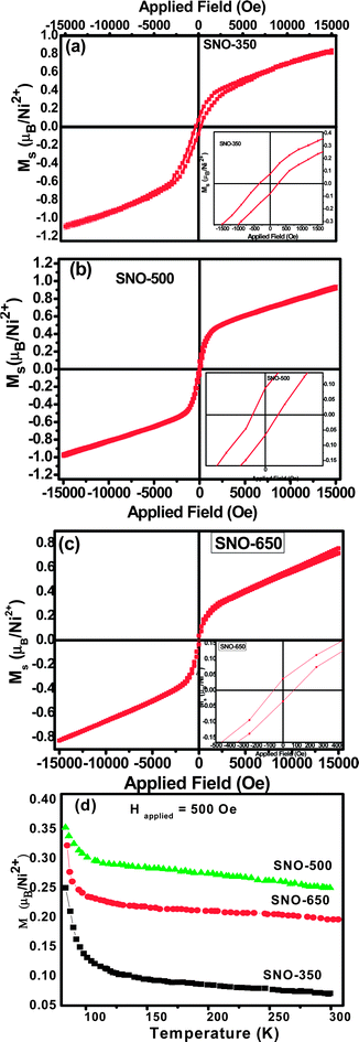 | ||
| Fig. 8 M–H curves of a) SNO- 350, b) SNO-500 and c) SNO-650 samples and d) M–T plot of all the Ni doped (5%) SnO2 nanorods annealed at different temperatures. | ||
| Sample code | SNO-350 | SNO-500 | SNO-650 | |
|---|---|---|---|---|
| VSM magnetization data | Ms (μB/Ni2+) | 0.818 | 0.925 | 0.758 |
| Hc (Oe) | 250 | 90 | 81 | |
| Mr (μB/Ni2) | 0.076 | 0.090 | 0.042 | |
| ESR data | Signal A at (mT) | 195.320 | 203.665 | 206.863 |
| g eff | 3.33 | 3.21 | 3.16 | |
| Surface rms roughness (5 × 5 μm2 area) | 39.18 | 30.61 | 150.8 | |
| Magnetic phase shift (Δφ) | 1.755° | 3.176° | 2.795° | |
Recently, several investigators studied extensively the role of oxygen vacancies in ODMS46–48 and attributed the ferromagnetism due to these defects. In order to understand the effects of oxygen vacancies associated with the surface defects on magnetic properties, ESR measurements have been carried out. Fig. 9 shows ESR spectra of all the samples of the present investigation. It is interesting to note that all the spectra are found to exhibit a broad resonance peak, denoted by the signal ‘A’ and the evaluated geff values for the signal ‘A’ are given in Table 4. With respect to the free radical DPPH (2,2-diphenyl-1-picrylhydrazyl, g = 2.00455), the Lande's g factor (geff) of the broad signal ‘A’ is found to be higher [in the range 3.16 to 3.33 (Table 4)]. It is interesting to note that the position of signal ‘A’ is located relatively at a lower field and is of a broad nature, indicating a clear ferromagnetic signature of the materials. With increasing the annealing temperature, the position of signal ‘A’ is found to shift towards the higher field side and the observed behaviour may be attributed to the decreasing ferromagnetic exchange interactions. Further, a gradual decrease in width of signal ‘A’ and geff values with increasing annealing temperature has been observed and the behaviour may be attributed to the variation of spin fluctuations or modification of long range exchange interactions. These results suggest that it may be possible to tune the behaviour of exchange interactions in these materials by controlling the oxygen vacancies through annealing temperature and the aspect ratio of nanograins. It is interesting to note that sample SNO-350 is found to exhibit a less intense peak at a point B (shown in Fig. 9) and is attributed to the unpaired electron spins, originating from the oxygen vacancies. In fact, shifting of line positions and changing of the widths of the broad resonance signals may not be due to the paramagnetic state of the samples. The intensity of signal ‘A’ is found to increase when compared with that of signal ‘B’ (Fig. 9), indicating that more magnetic domains might be participating in the ferromagnetic resonance phenomenon. These results are also in conformity with the VSM results. Therefore, it has been concluded that the intensity of ESR signals are found to be affected by not only the annealing temperature but also by surface anisotropy of the materials.
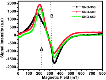 | ||
| Fig. 9 EPR spectra of Ni doped (5%) SnO2 nanorods annealed at different temperatures. | ||
It has also been evidenced from the ESR spectral analysis that the strength of exchange couplings between adjacent ferromagnetic grains depends on exchange media and its magnetic nature. Therefore, the nature of media becomes an extremely important parameter. Apart from this, the surface defects play an important role and may be responsible for the formation of magnetic or spin polarons. Further, these magnetic polarons are considered as isolated magnetic aggregates and influence the behaviour of exchanging media such as interface of inter-grains. Therefore, understanding of ESR spectra of these materials might be difficult. The variation in the width of signal ‘A’ with annealing temperature is also striking. The main contributions in modifying the width of resonance peaks originated from the effects of broadening due to variation of crystalline axes and random distribution of magnetic domains in the samples.
Magnetic force microscopy (MFM) measurements were also undertaken to confirm the ferromagnetism without Ni clusters. The magnetic phase images were recorded by two-pass technique (Lift Mode). After confirming the absence of a topography response, the magnetic phase images were recorded at room temperature in the scanning area of 5 × 5 μm2, by lifting the MFM tip to a predefined distance of 80 nm. Images 1 to 3 in Fig. 10(a) represent the initial topography images and images 1 to 3 in Fig. 10(b) represent MFM phase images for the same samples at an applied lift height of 80 nm. It can be noted that an attractive interaction leads to a negative phase shift (dark contrast in the image), while repulsive interactions give a positive phase shift (bright contrast). The observed bright and dark contrasts in the MFM images clearly indicate the formation of magnetic domains. It can be seen from Fig. 10 that the magnetic phase images (Fig. 10 (b): 1, 2, 3) do not match with the topography images (Fig. 10 (a): 1, 2, 3), indicating that the magnetic images are independent of the topography signals. Therefore, the observed magnetic phase shift may be due to the inherent magnetic nature of the samples. The magnetic domain pattern over the surface of the samples seems to show a strip or wave-like behaviour. The magnetic phase shift values (Δφ) of all the samples are given in Table 4. It can be seen that the magnetic phase shift, after an initial increase, is found to decrease with increasing annealing temperature and may be due to the variation in the effective magnetization of the samples. Further, from the MFM images the variation of dark contrasts is found to be small, which might have indicated a clear ferromagnetic behaviour without any trace of magnetic clusters at room temperature. All the MFM results are in agreement with the experimental results of VSM and ESR measurements. In fact, the effective ferromagnetic exchange interactions might have also linked with the unpaired electron spins originating from oxygen vacancies at the surface of nanorods. Therefore, to study the surface effects, surface roughness measurements were also undertaken, in the same corresponding area of the samples and the results are given in Table 4. It is interesting to note that with increasing annealing temperature up to 500 °C, the surface roughness is found to decrease with an increasing magnetic phase shift. On further increase of the annealing temperature up to 650 °C, the surface roughness is found to increase with decreasing the magnetic phase shift. This behaviour may be explained by the reduction of co-ordination at the surface between the local surface spin disorder and the support matrix system in which nanorods are dispersed, influencing the internal dipole–dipole interactions. It has been concluded from MFM studies that not only do the random distribution of Ni2+ ions but also the surface roughness influence the magnetic properties.
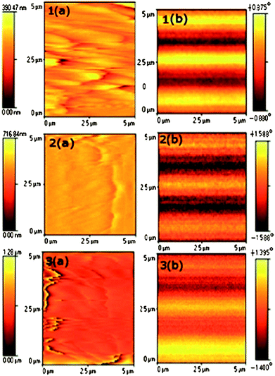 | ||
| Fig. 10 Room temperature MFM topography images (1(a) to 3(a)) before lift mode and MFM phase images (1(b) to 3(b)) after lift mode of Ni doped (5%) SnO2 samples annealed at temperatures of 1) 350, 2) 500 and 3) 650 °C. | ||
The understanding of the origin of ferromagnetism in ODMSs is quite complex and remains an open question. Therefore, an effort has been made to explain the phenomenon using the bound magnetic polarons (BMPs) model.49 The formation of BMPs depends on the available local oxygen vacancies near the Ni ions and is highly correlated with the interaction of the charge-transfer process between the bound magnetic polarons. In the samples of the present investigation, due to the substitution of Ni 2+ for Sn4+, a number of free charge carriers and oxygen vacancies might have been introduced to maintain the charge neutrality, leading to the formation of BMPs. The exchange interactions between these BMPs, which are coupled with the available small quantity of randomly distributed neighbouring Ni2+ ions leading to a strong long range ferromagnetic coherence of the localized bound magnetic polarons, might be responsible for the observed room temperature ferromagnetism. In fact, the effective interactions between BMPs depend on the dopant induced defects, the complex behaviour of exchange media and the distribution of Ni ions. However, extensive studies are still required to understand the local ferromagnetic behaviour and to exploit features of nanostructured spintronic devices with varying nanometric size and annealing temperature of Sn1−xNixO2−x nanorods. It can also be seen from the table that specific magnetization and remanence values after an initial increase are found to decrease with increasing annealing temperature and the observed behaviour may be attributed not only to the random distribution of Ni2+ ions but also to the variations in the number of BMPs. With increasing annealing temperature from 350 to 500 °C, the overlap of a large number of BMPs takes place leading to long-range magnetic exchange couplings with the available defect states, thereby enhancing the ferromagnetic activation. However, the magnetization value decreases on increasing the annealing temperature from 500 to 650 °C and the behaviour may be attributed to the decreasing effective coupling between BMPs and oxygen vacancies due to the surface diffusion behaviour of randomly distributed Ni ions. Thus, the aspect ratio and annealing temperature are crucial in controlling the surface morphology and structural disorder, which in turn influences their magnetic properties. Further, the coercivities (Hc) are found to decrease continuously with increasing aspect ratio indicating a clear influence of nanometric size on magnetic properties of the materials. This behaviour may be attributed to the increase of uncompensated spins in the surface and the magneto-crystalline anisotropy which in turn may lower the crystal symmetry at the grain boundaries. Thus, these studies clearly revealed that the confinement of nanometric grains and their surface morphology might have affected the coercitivity values of the samples.
Conclusions
In summary, single phase and high quality Ni doped (5%) SnO2 DMS nanorods were successfully synthesized by a simple PEG assisted wet chemical route. The results of the present work emphasize that PEG is an agent that causes heterogeneous nucleation due to its lower activation at the polymer/water interface and helps in the growth of Sn1−xNixO2−x nanorods. This process is a desirable way to overcome the limitation of the high solubility of dopants and the use of template. In the present investigation, M–H, M–T, ESR and MFM studies indicated clear RT ferromagnetism in all the samples without any impurity phases or clusters. The RT ferromagnetism might have originated due to the interactions among the dopant and defect induced percolated bound magnetic polarons in Sn1−xNixO2 single phase nanorods. The magnetic moment is found to decrease with decreasing oxygen vacancy concentration. As the annealing temperature effects, nanometric size, oxygen vacancies and the local electronic structure of the samples are interlinked with each other, the magnetic behaviour of the samples is not only dependent on the dopant and dopant distribution, but also on the sensitive behaviour of surface chemistry. The present investigation may also address important issues such as the behaviour of electronic structure and oxygen vacancies and the controllability of inter-diffusion and strain relaxation at the interfaces. These studies may be useful not only for a better understanding of various properties but also to design a better device. Further, by varying the aspect ratio of nanorods and annealing temperature, Ni doped (5%) tin oxide based DMSs may be useful in the exploration of magneto-optical, spintronic devices.Acknowledgements
The authors thank DRDO (ER & IPR), New Delhi, for providing financial assistance through a research project. The authors also thank the Department of Materials Research Centre, Indian Institute of Technology, Madras, for providing XPS and Raman measurements.References
- W. Prellier, A. Fouchet and B. Mercey, J. Phys.: Condens. Matter, 2003, 15, R1583 CrossRef CAS; S. J. Pearton, W. H. Heo, M. Ivill, D. P. Norton and T. Steiner, Semicond. Sci. Technol., 2004, 19, R59 CrossRef CAS; I. Djerdj, Z. Jagličić, D. Arčon and M. Niederberger, Nanoscale, 2010, 2, 1096 RSC; C. B. Fitzgerald, M. Venkatesan, L. S. Dorneles, R. Gunning, P. Stamenov and J. M. D. Coey, Phys. Rev. B: Condens. Matter Mater. Phys., 2006, 74, 115307 CrossRef.
- J. M. D. Coey, Curr. Opin. Solid State Mater. Sci., 2006, 10, 83 CrossRef CAS; S. J. Pearton, W. H. Heo, M. Ivill, D. P. Norton and T. Steiner, Semicond. Sci. Technol., 2004, 19, R59 CrossRef CAS.
- H. Ohno, Science, 1998, 281, 951 CrossRef; G. A. Prinz, Science, 1998, 282, 1660 CrossRef CAS.
- A. Wolf, D. D. Awschalom, R. A. Buhrman, J. M. Daughton, S. Von Molnar, M. L. Roukes, A. Y. Chtchelkanova and D. M. Treger, Science, 2001, 294, 1488 CrossRef CAS.
- S. D. Sarma, Nat. Mater., 2003, 2, 92 CrossRef CAS.
- X. Huang, A. Makma, J. R. Chelikowsky and L. Kronik, Phys. Rev. Lett., 2005, 94, 236801 CrossRef.
- Q. Xu, L. Hartmann, S. Zhou, A. Mcklich, K. Potzger, M. Helm, G. Biehne, H. Hochmuth, M. Lorenz, M. Grundmann and H. Schmidt, Phys. Rev. Lett., 2008, 101, 076601 CrossRef.
- S. Han, D. Zhang and C. Zhou, Appl. Phys. Lett., 2006, 88, 133109 CrossRef.
- A. Punnoose, K. M. Reddy, J. Hays, A. Thurber and M. H. Engelhard, Appl. Phys. Lett., 2006, 89, 112509 CrossRef.
- Liu Xiaofang, Iqbal Javed, Wu Zhangben, He Bo and Yu Ronghai, J. Phys. Chem. C, 2010, 114, 4790 CrossRef.
- J. Sakuma, K. Nomura, C. Barrero and M. Takeda, Thin Solid Films, 2007, 515, 8653 CrossRef CAS.
- X. F. Liu and R. H. Yu, J. Appl. Phys., 2007, 102, 083917 CrossRef.
- B. Straumal, B. Baretzky, A. Mazilkin, S. Protasova, A. Myatiev and P. Straumal, J. Eur. Ceram. Soc., 2009, 29, 1963 CrossRef CAS.
- N. H. Hong, A. Ruyter, W. Prellier, J. Sakai and N. T. Huong, J. Phys.: Condens. Matter, 2007, 17, 6533.
- Paul I. Archer, Pavle V. Radovanovic, Steve M. Heald and Daniel R. Gamelin, J. Am. Chem. Soc., 2005, 127, 14479 CrossRef.
- L. Chun-Ming, F. Li-Mei, Zu Xia-Tao and Z. Wei-Lie, Chin. Phys., 2007, 16, 95 CrossRef.
- C. M. Liu, L. M. Fang, X. T. Zu and W. L. Zhou, Phys. Scr., 2009, 80, 065703 CrossRef.
- L. Lutterotti, Maud Cpd, Newsletter (IUCr), 2000, 24 Search PubMed; L. Lutterotti, S. Matthies and H.– R. Wenk, MAUD (Material Analysis Using Diffraction): a user friendly Java program for Rietveld Texture Analysis and more, Proceeding of theTwelfth International Conference on Textures of Materials (ICOTOM-12), 1999, 1, 1599 Search PubMed.
- H. Matsuhata, J. Gjønnes and J. Taftø, Acta Crystallogr., Sect. A: Found. Crystallogr., 1994, 50, 115 CrossRef.
- W. Z. Wang, G. H. Wang, X. S. Wang, Y. J. Zhan, Y. K. Liu and C. L. Zheng, Adv. Mater., 2002, 14, 67 CrossRef CAS; J. J. Zhu, X. H. Liao, X. N. Zhao and H. Y. Chen, Mater. Lett., 2001, 49, 91 CrossRef CAS.
- C. M. Liu, X. T. Zu, Q. M. Wei and L. M. Wang, J. Phys. D: Appl. Phys., 2006, 39, 2494 CrossRef CAS.
- F. Gu, S. F. Wang, C. F. Song, M. K. Lu, Y. X. Qi, G. J. Zhou, D. Xu and D. R. Yuan, Chem. Phys. Lett., 2003, 372, 451 CrossRef CAS; J. X. Zhou, M. S. Zhang, J. M. Hong, J. L. Fang and Z. Yin, Appl. Phys. A: Mater. Sci. Process., 2005, 81, 177 CrossRef CAS.
- Yingkai Liu, Yi Dong and Guanghou Wang, J. Appl. Phys., 2003, 82, 260 CAS.
- C. Xu, G. Ding Xu, Y. Liu, X. Zhano and G. Wang, Scr. Mater., 2000, 46, 789; Bin Cheng, Joette M. Russell, Wensheng Shi, Lei Zhang and Edward T. Samulski, J. Am. Chem. Soc., 2004, 126, 5972 CrossRef CAS.
- F. Gervais and W. Kress, Phys. Rev. B:, 1985, 31, 4809 CrossRef CAS.
- R. J. Nemanich, S. A. Solin and R. M. Martin, Phys. Rev. B:, 1981, 23, 6348 CrossRef CAS.
- Feng Gu, Shufen Wang, Hongming Cao and Chunzhong Li, Nanotechnology, 2008, 19, 095708 CrossRef.
- A. Dieguez, A. Romano-Rodriguez, A. Vila and J. R. Morante, J. Appl. Phys., 2001, 90, 1550 CrossRef CAS.
- S. K. Soumen Das and Subhadra Chaudhuri, J. Appl. Phys., 2006, 99, 14303 CrossRef.
- Bin Cheng, Joette M. Russell, Wensheng Shi, Lei Zhang and Edward T. Samulski, J. Am. Chem. Soc., 2004, 126, 5972 CrossRef CAS.
- C. D. Wagner, W. M. Riggs, L. E. Davis and J. E. Moulder, in Handbook of X-Ray Photoelectron Spectroscopy, ed. G. E. Muilenberg, Perkin-Elmer, Physical Electronics, Eden Prairie, MN, 1979 Search PubMed.
- Handbook of X –ray Photoelectron Spectroscopy, ed. J. F. Moulder, W. F. Stickle, P. E. Sobol, K. D. Bomben, J. J. Chastain and R. C. King, Physical Electronics, Eden Prarie, MN, 1995 Search PubMed.
- G. H. Yu, L. R. Zeng, F. W. Zhu, C. L. Chai and W. Y. Lai, J. Appl. Phys., 2001, 90, 4039 CrossRef CAS.
- G. H. Yu, F. W. Zhu and C. L. Chai, Appl. Phys. A: Mater. Sci. Process., 2003, 76, 45 CrossRef CAS.
- Hui-Hsin Tseng, Ming-Chi Wei, Shao-Fan Hsiung and Chih-Wei Chiou, Chem. Eng. J., 2009, 150, 160 CrossRef CAS.
- Y. Nagasawa, T. Choso, T. Karasuda, S. Shimomura, F. Ouyang, K. Tabata and Y. Yamaguchi, Surf. Sci., 1996, 433–435, 226.
- Takashi Kawabe, Kenji Tabata, Eiji Suzuki, Yoichi Yamaguchi and Yousuke Nagasawa, J. Phys. Chem. B, 2001, 105, 4239 CrossRef CAS.
- Amorphous and Liquid Semiconductor, ed. J. Tau, Plenum Press, New York, 1974p. 159 Search PubMed; J. I. Pankove, in Optical Processes in Semiconductors, Prentice Hall, Englewood Cliffs, NJ, 1971 Search PubMed.
- J. D. Ye, S. L. Gu, S. M. Zhu, S. M. Liu, Y. D. Zheng, R. Zhang, Y. Shi, Q. Yuand and Y. D. Ye, J. Cryst. Growth, 2005, 283, 279 CrossRef CAS.
- J. Jin, P. C. Seong, I. C. Cha, C. S. Dong and S. P. Jin, Solid State Commun., 2003, 127, 595 CrossRef.
- Ch. Kittel, Introduction to Solid State Physics, Wiley, New York, 7th edn, 1996 Search PubMed.
- Y. Ichiyanagi, N. Wakabayashi, J. Yamazaki, S. Yamada, Y. Kimishima, E. Komatsu and H. Tajima, Phys. B, 2003, 329, 862 CrossRef.
- J. T. Richardson and W. O. Milligan, Phys. Rev., 1956, 102, 1289 CrossRef CAS.
- R. H. Kodama, S. A. Makhouf and A. E. Berkowitz, Phys. Rev. Lett., 1997, 78, 1393 CrossRef.
- D. A. Schwartz, K. R. Kittilstved and D. R. Gamelin, Appl. Phys. Lett., 2004, 85, 1395 CrossRef CAS.
- J. M. D. Coey, A. P. Douvalis, C. B. Fitzgerald and M. Venkatesan, Appl. Phys. Lett., 2004, 84, 1332 CrossRef CAS.
- R. Suryanarayanan, V. M. Naik, P. Kharel, P. Talagala and R. Naik, J. Phys.: Condens. Matter, 2005, 17, 755 CrossRef CAS.
- N. H. Hong, J. Sakai, N. T. Huong, N. Poirot and A. Ruyter, Phys. Rev. B: Condens. Matter Mater. Phys., 2005, 72, 45336 CrossRef.
- C. B. Fitzgerald, M. Venkatesan, L. S. Dorneles, R. Gunning, P. Stamenov and J. M. D. Coey, Phys. Rev. B: Condens. Matter Mater. Phys., 2006, 74, 15307; J. M. D. Coey, M. Venkatesan and C. B. Fitzgerald, Nat. Mater., 2005, 4, 173 CrossRef CAS; J. Wang, Z. Gu, M. Lu, D. Wu, C. Yuan, S. Zhang, Y. Chen, S. Zhu and Y. Zhu, Appl. Phys. Lett., 2006, 88, 252110 CrossRef.
| This journal is © The Royal Society of Chemistry 2011 |