Rapidly synthesized ZnO nanowires by ultraviolet decomposition process in ambient air for flexible photodetector†
Jyh Ming
Wu
*a,
Yi-Ru
Chen
a and
Yu-Hung
Lin
b
aDepartment of Materials Science and Engineering, Feng Chia University, 100 Wenhwa Rd, Seatwen, Taichung 40724, Taiwan. E-mail: jmwu@fcu.edu.tw; Fax: (+886) 4-24510014; Tel: (+886) 4-24517250 ext: 5316
bDepartment of Materials Science and Engineering, National Tsing Hua University, Hsinchu 300, Taiwan
First published on 14th December 2010
Abstract
We are the first group to use a simple direct ultraviolet light (UV, λ = 365 nm, I = 76 mW cm−2) in a decomposition process to fabricate ZnO nanowires on a flexible substrate using a zinc acetylacetonate hydrate precursor in ambient air. ZnO nanocrystal (or nanowire) production only requires three to ten minutes. A field emission scanning electron microscopy (FESEM) image reveals a high aspect ratio of the ZnO nanowires, which are grown on a substrate with a diameter of ∼50–100 nm, and a length of up to several hundred microns. High resolution transmission electron microscopy (HRTEM) images reveal that the nanowires consist of many single crystalline ZnO nanoparticles that grow along the c axis, which suggests an oriented attachment process. A potential application for flexible UV photodetectors was investigated using a UV lamp (λ = 365 nm, I = 2.34 mW cm−2). A significant ratio of photocurrent to dark current—around 11![[thin space (1/6-em)]](https://www.rsc.org/images/entities/char_2009.gif) 300%—was achieved.
300%—was achieved.
1. Introduction
Zinc oxide (ZnO) nanowires are n-type semiconductors with a wide direct band gap of 3.34 eV and have been demonstrated to be applicable to UV lasers,1 photovoltaic solar cells,2 nanogenerators,3 and ultraviolet (UV) photodiodes,4 due to their large excitation binding energy of 60 meV. However, to fabricate these nanodevices for commercial applications, low temperature, low cost and large area synthesized processing is key to industrial production.Vapor transfer in the thermal evaporation process is favored to produce high-quality ZnO nanowires due to its simplicity. However, this process generally requires high temperatures to achieve single-crystal semiconductors, thereby limiting the quality of electronics on alternative substrates.5 Although a low-temperature (i.e. 95–200 °C) hydrothermal process can produce high-quality single crystalline ZnO nanowires, a relatively complex process with long processing time is required in comparison with our newly developed UV decomposition process.
Recently, a UV photodetector made from ZnO nanowires has been widely reported. However, a high sensitivity (ratio of photocurrent to dark current) flexible photodetector has rarely been investigated. It is of great interest to develop a process with a low working temperature, short processing time, low cost, and high throughput to fabricate large area ZnO nanowire surfaces. Solution approaches to ZnO nanowires are appealing because of their low growth temperatures and potential for scale-up.6,7
As Zn(AcAc)2 possesses a low decomposition temperature (T < 200 °C), it has been proven to be a suitable single-source precursor for the growth of ZnO nanostructures by metal–organic chemical vapour deposition (MOCVD), and a substrate at a controlled temperature of ∼500–600 °C.8 Fauteux et al. first developed a laser-assisted technique (CO2 laser, λ = 10.6 μm) for the surface-bound growth of ZnO nanostructures.9 Single crystalline ZnO nanorods can be produced using laser-induced decomposition of a Zn(AcAc)2 precursor. The growth conditions of the ZnO nanostructures depend on the laser beam intensity profile and the temperature gradient of the reaction zone. Fauteux et al. also revealed that the laser beam intensity profile induces a temperature gradient in the reaction zone, which may contribute to the instability of the heating process and the evaporation of the solvents. These methods provide useful information for application in future research.
In this work, an UV-light decomposition process was employed for the first time in the fabrication of ZnO nanowires on a large-area (∼5 × 5 cm) flexible substrate (polyimide, PI; or polyethersulfone, PES) in ambient air. TEM images confirmed that the polycrystalline ZnO nanowires consist of single-crystalline ZnO nanoparticles, ∼5–20 nm in diameter. The ZnO nanoparticles aggregated to form one dimensional nanowires by oriented attachment, which advances growth along the c axis. The UV photon-sensing measurements showed that the as-prepared ZnO nanowires on a flexible substrate exhibit a high photon-sensitivity (IUV-on/IUV-off) of 113 fold. The as-developed process was simple, short (only three to ten minutes), had good photo-sensing properties, and was a straightforward process for fabricating large-area flexible substrates. This implies that it has good potential for integration into the portable electronic devices.
2. Experimental
Zinc acetylacetonate hydrate powder (0.4 g, ZnC10H14O4·H2O or Zn(AcAc)2·H2O, Strem, purity 98%) was mixed with ∼2 ml each of deionized (DI) water and denatured ethanol (EtOH 85.47%, MeOH 13.68%, ErOAc 0.85%, 95%), and then stirred for three to ten minutes to produce the Zn(AcAc)2·H2O precursor.9 As-prepared flexible substrates (i.e. polyimide, PI; or polyethersulfone, PES) were cleaned with ethanol and DI water ultrasonically for ∼10–15 min. The Zn(AcAc)2·H2O precursor was then spin coated onto a flexible substrate. UV-light with an intensity of 76 mW cm−2 (λ = 365 nm) was used to decompose the Zn(AcAc)2 precursor for three to ten minutes to fabricate the ZnO nanowires. Fig. 1 shows the synthesis process and its products.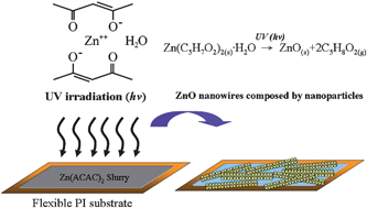 | ||
| Fig. 1 Schematic diagram of the synthesis process and the molecular structure of Zn(ACAC)2 precursor. | ||
The structure of the sample was characterized using a thin-film X-ray diffractometer (XRD, Bruker). The sample morphology and crystalline structure were characterized by field emission scanning electron microscopy (FESEM, HITACHI, S-4800) and high resolution transmission emission microscopy (HRTEM, JEOL, JEM-3000F). The chemical nature of the ZnO nanowires was evaluated by high resolution X-ray photoelectron spectroscopy (HRXPS, ULVAC-PHI, AES 650) using mono aluminium. A UV lamp (λ = 365 nm, I = 2.34 mW cm−2) acted as the excitation source during photoelectric current measurements to investigate the UV sensing properties of an as-prepared flexible UV photodetector.
3. Results and discussion
Fig. 2(a) shows that the nanowires can be spin-coated on a flexible substrate with a large area of ∼5 × 5 cm, after which transparency is observed. The inset image of Fig. 2(a) shows that the nanowires were successfully fabricated on the flexible substrate. A mechanical test was then performed ∼20 times, bending the ZnO nanowire/flexible substrate into a curve with a radius of ∼10 mm. It was demonstrated that the nanowire/flexible substrate does not exhibit peeling behavior. Fig. 2(b) shows that the nanowires grown on the flexible substrate had a high aspect ratio. The inset image of Fig. 2(b) shows that the nanowire diameter is ∼50–100 nm, and the length is up to several hundred microns. The XRD in Fig. 2(c) shows that the as-synthesized nanowires exhibit a single phase of ZnO hexagonal (wurtzite) crystalline structures with lattice constants a = 0.325 nm and c = 0.52 nm (JCPDS 36-1451).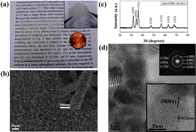 | ||
| Fig. 2 (a) ZnO nanowires synthesized on 5 × 5 cm flexible substrate with transparency. Inset image: bendable nanowires on plastic substrate; (b) FESEM image of ZnO nanowires; inset image: single nanowires with diameter of ∼100 nm; (c) XRD pattern of the as-synthesized ZnO nanowires; (d) TEM images revealed that nanowires consist of nanoparticles ∼5–20 nm in diameter. The inset image in the lower right-hand corner reveals a single crystalline ZnO nanoparticle. The certain lattice spacing is ∼0.52 nm. Inset image in the upper right-hand corner is the SAD pattern. | ||
The low magnitude TEM image in Fig. 2(d) reveals that the polycrystalline ZnO nanowires consist of many ZnO single-crystalline nanoparticles, ∼5–20 nm in diameter. The lower right-hand corner inset image of Fig. 2(d) shows a nanoparticle of a single crystalline structure, with a certain lattice spacing of ∼0.52 nm, which corresponds to the [0001] axis. Thus, we can conclude that the as-prepared ZnO nanowires consist of fine single crystalline nanoparticles and grow along the [0001] axis. The inset image in the upper right-hand corner of Fig. 2(d) shows that the selected-area electron diffraction (SAD) pattern is taken from multiple nanoparticles. This indicates that the ZnO nanowires belong to the wurtzite phase of polycrystalline structures.
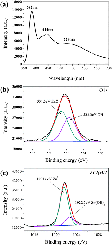
The photoluminescence (PL) spectrum of Fig. 3(a) shows a highly intense blue emission peak at 382 nm,10 which is attributed to excitonic recombination corresponding to the near-band-edge emission in the ZnO nanocrystals.11 Two broad peaks at 444 nm and 528 nm correspond to the oxygen vacancies and deep levels,12 respectively. Oxygen vacancies can produce a shallow defect donor level which is located below the conduction band at ∼0.5 eV (∼430–465 nm).13 Wen et al. reported that the peak at 528 nm can be attributed to the transition from the conduction band to Ozn, which has a band gap of ∼2.35 eV.14 We therefore suggest that excess Zn2+ is produced during the reaction process of UV decomposition according to the following equations:
 | (1) |
 | (2) |
 | (3) |
 | ||
| Fig. 3 (a) PL spectrum of the as-synthesized ZnO nanowires; (b) XPS spectrum, deconvolution of the O1s core-level spectrum into two peaks, ZnO at 531.3 eV and OH at 532.3 eV; (c) XPS spectrum, deconvolution of the Zn2p3/2 core-level spectrum into two peaks, Zn2+ at 1021.6 eV and Zn(OH)2 at 1022.7 eV. | ||
Eqn (1) demonstrates that the Zn(C5H7O2)2·H2O reacted with water molecules to produce the Zn2+ ions and OH species. These further reacted with each other to produce the excited state of Zn(OH)*2 with H2O, as shown in eqn (2). Eqn (3) explains the further dissociation of excited-state Zn(OH)*2 into ZnO with H2O byproducts. Although eqn (1) and (2) demonstrate the formation process of ZnO nanocrystals, this reaction is evidence that the excess Zn2+ ions produce and form the defect centers, resulting in the appearance of a green emission in ZnO nanowires. Accordingly, the PL spectrum reveals an emission band at ∼528 nm, which is attributed to Zn-related band emission in the ZnO nanocrystals.
However, eqn (1) also demonstrates that the byproduct of C5H8O2 with OH species was produced during the decomposition of the Zn(C5H7O2)2(s)·H2O precursor. The melting point of the byproduct C5H8O2, which can be decomposed with UV light at room temperature leaving hydroxyl bonds on the surface of nanowires, is −23 °C.15 To investigate the bonding species of the as-synthesized ZnO nanowires, after sputtering XPS was employed to verify the O1s spectrum. The O1s core-level spectrum can be deconvoluted into two peaks, 531.3 eV13 and 532.3 eV,16 which correspond to the ZnO and OH species, respectively, as shown in Fig. 3(b). This verifies that the OH hydroxyl formed on the surfaces of the ZnO nanowires during crystal growth. Fig. 3(c) shows that the Zn2p3/2 peak can be deconvoluted into two peaks, 1021.6 eV and 1022.7 eV, which correspond to the Zn2+ and Zn(OH)2 species,17,18 respectively. This is evidence suggests that the Zn(OH)2 and hydroxyl (OH) species formed on the surface of the ZnO nanoparticles as the UV decomposed the Zn(AcAc)2 precursor.
In this work, the ZnO nanoparticles aligned to form nanowires in a self-assembly process. The growth of one dimensional ZnO nanowires usually results from different surface energies of the respective lattice planes.19 Pacholski et al. reported that the oriented attachment of preformed quasi-spherical ZnO nanoparticles is a major reaction path during the formation of single crystalline nanorods.20 This mechanism is based on self-assembling primary nanoparticles (nanodots) which perform lattice fusion and spontaneously adjust to the adjacent crystallographic planes.21,22 In this work, TEM images were used to observe the formation process of the nanowires at different UV decomposition times. First, the ZnO nanowires showed that several nanoparticles aggregated together at the initial stage of 3 min, as shown in Fig. 4(a). Fig. 4(b) shows that the nanoparticles (marked A, B, and C) were fused by oriented attachment after 5 min of UV decomposition treatment. Following a 10 min treatment process, there was an increase in the elongation of the nanoparticles along the c axis [0001], as shown in Fig. 4(c). A clear lattice fringe of ∼0.52 nm appeared, as shown in the inset image of Fig. 4(c). However, the elongation of nanoparticles was not as strong from 3–5 min (see Fig. 4(a)–(b)), suggesting that the annealing time is not enough. At 10 min, elongations of nanoparticles along the c axis formed gradually. After 40 min of annealing, the HRTEM image in Fig. 4(d) shows that the elongation of nanoparticles along the c axis is more significant in comparison with the samples at 3, 5, and 10 min produced by the UV-light decomposition process. Thus, with increasing annealing time the growth of ZnO nanowires along the c axis becomes more significant. This is evidence that the formation of ZnO nanowires is followed by an oriented attachment process. This experimentally demonstrates why nanoparticles aggregate and align with each other to grow along the c axis. The corresponding FESEM images for UV-light decomposition at 3, 5, 10, and 40 min are shown in the ESI† Fig. S1. It is clear that aggregation of nanowires into bundles increased with annealing time. However, the nanowires still consisted of nanoparticles. We suggest that the bundling of aligned nanowires is attributed to the surface tension effect as reported by Lau et al.23
![(a) The nanoparticles aggregated together during the initial three minutes of the first stage. (b) After 5 min, ZnO nanoparticles fused to each other; A, B, and C. (c) After 10 min of oriented attachment, several nanoparticles fused to form a preferred orientation along the [0001] axis. A lattice fringe of ∼0.52 nm is in the inset. (d) After 40 min, the elongation of nanoparticles along the c axis is more significant.](/image/article/2011/NR/c0nr00595a/c0nr00595a-f4.gif) | ||
| Fig. 4 (a) The nanoparticles aggregated together during the initial three minutes of the first stage. (b) After 5 min, ZnO nanoparticles fused to each other; A, B, and C. (c) After 10 min of oriented attachment, several nanoparticles fused to form a preferred orientation along the [0001] axis. A lattice fringe of ∼0.52 nm is in the inset. (d) After 40 min, the elongation of nanoparticles along the c axis is more significant. | ||
A corresponding schematic diagram of oriented attachment is shown in Fig. 5. UV light was used to decompose the Zn(AcAc)2·H2O precursor, which became ZnO nuclei with Zn(OH)2. At an early stage, the high surface energy of the nanoparticles caused quasi-spherical particles to aggregate together, thus reducing their free energy. After that, the nanoparticles fused together, elongating along the c axis, which is due to a more thermodynamically stable plane of (0001) along the c axis. This or other growth directions may also appear along other crystal orientations.20 Growth direction is determined by the nanoparticles that are adsorbed by different amounts of counterions (ion species, i.e. OH−). The result is different surface charges that could hinder or favor oriented attachment, which requires intimate contact with the respective surface planes. Sun et al. reported that the growth of ZnO nanorods are deduced to be Zn-polar, but can be either Zn-atom or O-atom terminated.24 The ZnO nanocrystals present the Zn- or O-atoms and terminated Zn-polar (0001) faces, which serve to nucleate the subsequent growth of ZnO nanowires. The different surface terminations result from the electrostatic interactions. Nanowire morphologies are determined by the alteration of the concentration ratios of Zn2+/OH− (and ZnOH+/OH−). Our work is similar to the mechanism of oriented attachment, first reported by Penn and Banfield.25 Although the XRD pattern showed that the (0001) plane was not significantly sharper than the other planes, the growth of nanowires along the c axis was significant (see SEM and TEM images above, Fig. 2 and Fig. 4 respectively). This can be attributed to the fact that the surface of ZnO nanoparticles possesses a large concentration of Zn(OH)2, which further dissociates into ZnO nuclei with H2O (see eqn (3) above). During the UV decomposition process, due to a large amount of ZnO nuclei precipitated from Zn(OH)2 on the intergranular boundaries (grain boundaries), the resulting elongation of the nanoparticles along the c axis was not obvious, as there was not enough time to undergo an oriented attachment process. Pacholski reported that the refluxing process should take a long time in order to yield high-quality rod-like nanocrystals. This work proposes a short processing time without the Zn(OH)2 being continuously supplied to the substrate during the crystal growth process. Therefore, the growth of single-crystal nanorods due to oriented attachment was terminated, as opposed to creating the polycrystalline ZnO nanowires. The detailed formation process is under investigation and further experiments are needed to clarify the formation mechanism.
 | ||
| Fig. 5 A schematic diagram of oriented attachment process. | ||
Fig. 6(a) shows a flexible UV photodetector and its corresponding schematic diagram. The sensitivity, S, is defined as IUV-on/IUV-off. IUV-on is the sensor's photocurrent as the UV lamp (2.34 mW cm−2) switches to the on state, while IUV-off is the sensor's dark current as the UV lamp switches to the off-state. Following exposure of the ZnO nanowires to the irradiation of the UV lamp, the photocurrent in ZnO nanowires increased from 2.23 × 10⁻⁹ A to 2.51 × 10⁻⁷ A and gradually reached saturation, as shown in Fig. 6(b). This is due to the slow charge transfer process across the boundaries of the nanowires (see details below).26 When the UV lamp is in an off state, the photocurrent decreases to reach its initial state.27 The sensitivity for the as-synthesized ZnO nanowires is 113 fold (i.e. 10-minute sample). As we investigated the annealing sample from 3–40 min (see ESI† Fig. S2), the sensitivity increased with increasing UV decomposition time. This can be attributed to the defect states on the surface of the nanoparticles reacting with ambient air and being consumed. The sensitivity increased with increasing UV decomposition time, especially from 3–10 min. A maximum sensitivity of ∼140 fold occurred at 40 min. To improve the sensing properties, in addition to increases in the annealing time, recently some authors have reported that Schottky barrier electrodes improve the sensor performance.28–30 This will be investigated by conducting further experiments.
 | ||
| Fig. 6 (a) A flexible UV photodetector with its schematic diagram. (b) Photoresponse as function of time during switching of UV on/off states. | ||
In this work, a high contrast ratio of photocurrent to dark current in flexible ZnO nanowires—∼11300% (i.e.10-minute sample)—was observed. To explain this phenomenon, a semi-quantitative model for nanowire conduction can be developed (Fig. (7)).31 The conductance change in the nanowires can be regarded as shown in eqn (4):
| G = G0exp(−qψs/kT) | (4) |
 | ||
| Fig. 7 Barrier at intergranular ZnO nanoparticles, (a) UV off and (b) UV on. | ||
The activation energy, qψs, is located in the intergranular space and is the same for all nanocrystals. k is the Boltzmann constant while T is the absolute temperature. In this case, the sensitivity rises because electrons must overcome the barrier qψs. Thus, the conductance varies exponentially with the barrier height. The barrier is strongly dependent on the ambient gas conditions, being slow in a vacuum and fast in air.32
According to the XPS data above, to synthesize the ZnO nanowires using a UV decomposition process, the hydroxyl (OH) groups are usually present on the surface of solid oxides unless the surface is treated at elevated temperatures.33 It should be noted that ZnO nanowires are synthesized by a conventional high temperature vapor transfer process (i.e. 500–600 °C), which incorporates the OH species into the host lattices, leading to a sensing activity mainly ascribed to O species in ambient air.34,35 In contrast, our product is synthesized in a low-temperature process of UV-decomposition, which leaves behind many OH species (see XPS spectra of Fig. 3(b) above) on the surface of the product. Therefore, the low conductivity of ZnO nanowires under UV-off can be ascribed to the additional OH species which combine with O and are adsorbed on these nanoparticles (see details below). When the UV lamp is switched to an off state, the reactions can be described by eqn (5) and (6). The O and OH species extract the free electrons from the conduction band of ZnO nanocrystals and become O− and OH− ions to be adsorbed on the surface of the ZnO nanocrystals.
| O + e− → O− | (5) |
| OH + e− → OH− | (6) |
| Oo → ½O2 + 2V••o + 2e′ | (7) |
The PL spectrum demonstrated that the as-synthesized ZnO nanowires exhibited a high concentration of oxygen deficiency. The free carriers can be generated from the chemical reaction between oxygen and oxygen defects (oxygen vacancies, V••0) and are located in the conduction band of ZnO, as shown by the chemical reaction in eqn (7). Thus, the oxygen and hydroxyl extracted the electrons from the conduction band of ZnO and were chemisorbed on the surface of the nanowires, causing the space charge layer (depletion layer) to become thick, as shown in Fig. 7(a). In other words, the electrons are trapped in intergranular nanoparticle space by adsorbed oxygen and hydroxyl species, resulting in an increase of qψs, which increases the resistivity of the ZnO nanowires. The depletion layer is formed at the surface where conduction band electrons are trapped, and charge donors are formed near the semiconductor surface.32 However, the nanowires consisted of nanoparticles of ∼5–20 nm (see HRTEM image above) in diameter and provided appreciable adsorption sites on the intergranular surface, contributing considerably to the reactivity on these surfaces. This gives a reasonable explanation as to why a low conductivity of 2.23 × 10⁻⁹ A was obtained for ZnO nanowires when the UV lamp was off.
Upon exposure to the UV lamp, photo-generated holes migrated to the surface and discharged the adsorbed O− and OH−. The reactions can be regarded as eqn (8), (9).
| h+ + 2OH− → H2O + ½O2 + e− | (8) |
| h+ + O−2 → O | (9) |
The adsorbed OH− and O− ions were discharged to form the O (or O2) and H2O species and then released into ambient air. The released electrons simultaneously went back into the conduction band of ZnO nanocrystals, causing decreases in the width and height of barrier, as shown in Fig. 7(b). Thus, the photocurrent exponentially increased until saturation. The released electrons returned to the semiconductor surface, resulting in an enhanced density of charge carriers, causing the Femi-level to return to just below the conduction band and reducing the depletion layer. This gives an explanation for why a high conductivity of 2.51 × 10⁻⁷A was obtained for ZnO nanowires when the UV lamp was on. However, the barrier of qψs blocks the electron flow, controls the electron transport properties and is tunable by particle size with absorbed species (i.e. O− and OH−), enhancing the sensitivity of the sensor.36 The sensor's sensitivity therefore exhibited exponential behavior during the switching between the UV lamp's on and off states.
The as-prepared ZnO nanowires consisted of small particles which adsorb additional OH species, resulting in the ZnO nanowire device exhibiting a large ratio of photocurrent to dark current (∼a magnitude of two orders) when exposed to UV on and off. The ZnO nanowires were spin-coated on a plastic substrate, which holds promise for flexible photodetector applications.
4. Conclusions
In summary, a UV photodetector of ZnO nanowires can be directly fabricated on a flexible substrate using a UV decomposition process under ambient air, with rapid synthesis in only ten minutes. HRTEM shows that the ZnO nanowires consisted of single crystalline nanoparticles, 5–20 nm in diameter. The ZnO nanocrystals were aligned to fuse into one dimensional nanowires by oriented attachment. The as-prepared ZnO nanowires consisted of small particles which adsorbed additional OH species, such that the ZnO nanowire device exhibited a large ratio of photocurrent to dark current when exposed to UV on and off. A high sensitivity ratio of photocurrent to dark current of 113 fold (i.e. 10-minute sample) was obtained, revealing that the as-synthesized ZnO nanowires possess high potential for applications in UV photodetectors and optical switches. The UV decomposition process developed here is very simple, with a large area and short processing time, making it suitable for mass production.Acknowledgements
The authors would like to thank the National Science Council of the Republic of China for financially supporting this research under Contract No. NSC 97-2221-E-035-004 and NSC 98-2221-E-035-008.Reference
- P. Yang, H. Yan, S. Mao, R. Russo, J. Johnson, R. Saykally, N. Morris, J. Pham, J. R. He and H. J. Choi, Adv. Funct. Mater., 2002, 12, 323 CrossRef CAS.
- J. Tornow and K. Schwarzburg, J. Phys. Chem. C, 2007, 111, 8692 CrossRef CAS.
- Z. L. Wang and J. Song, Science, 2006, 312, 242 CrossRef CAS.
- Z. Zhu, L. Zhang, J. Y. Howe, Y. Liao, J. T. Speidel, S. Smith and H. Fong, Chem. Commun., 2009, 2568 RSC.
- M. C. McAlpine, R. S. Friedman and C. M. Lieber, Proc. IEEE, 2005, 93, 1357 CrossRef CAS.
- L. E. Greene, M. Law, J. Goldberger, F. Kim, J. C. Johnson, Y. Zhang, R. J. Saykally and P. Yang, Angew. Chem., Int. Ed., 2003, 42, 3031 CrossRef CAS.
- B. D. Yao, Y. F. Chan and N. Wang, Appl. Phys. Lett., 2002, 81, 757 CrossRef CAS.
- J. J. Wu and S. C. Liu, Adv. Mater., 2002, 14, 215 CrossRef CAS.
- C. Fauteux, R. Longtin, J. Pegna and D. Therriault, Inorg. Chem., 2007, 46, 11036 CrossRef CAS.
- Q. H. Li, Q. Wan, Y. X. Liang and T. H. Wang, Appl. Phys. Lett., 2004, 84, 4556 CrossRef CAS.
- Z. Wang, J. Gong, Y. Su, Y. Jiang and S. Yang, Cryst. Growth Des., 2010, 10, 2455 CrossRef CAS.
- A. B. Djurišić, W. C. H. Choy, V. A. L. Roy, Y. H. Leung, C. Y. Kwong, K. W. Cheah, T. K. Gundu Rao, W. K. Chan, H. F. Lui and C. Surya, Adv. Funct. Mater., 2004, 14, 856 CrossRef CAS.
- Y. R. Ryu, S. Zhu, J. D. Budai, H. R. Chandrasekhar, P. F. Micli and H. W. White, J. Appl. Phys., 2000, 88, 201 CrossRef CAS.
- F. Wen, W. Li, J. H. Moon and J. H. Kim, Solid State Commun., 2005, 135, 34 CrossRef CAS.
- CRC Handbook of Chemistry and Physics. “Physical Constant and Organic Compounds” , Section 3, 3–574 Search PubMed.
- C. Jones and E. Sammann, Carbon, 1990, 28, 509 CrossRef CAS.
- S. P. Kowalczyk, R. A. Pollak, F. R. McFeely, L. Ley and D. A. Shirley, Phys. Rev. B: Solid State, 1973, 8, 2387 CrossRef CAS.
- L. S. Dake, D. R. Baer and J. M. Zachara, Surf. Interface Anal., 1989, 14, 71 CrossRef CAS.
- Z. L. Wang, Appl. Phys. A: Mater. Sci. Process., 2007, 88, 7 CrossRef CAS.
- C. Pacholski, A. Kornowski and H. Weller, Angew. Chem., Int. Ed., 2002, 41, 1188 CrossRef CAS.
- Y. Zhang, F. Lu, Z. Wang and L. Zhang, J. Phys. Chem. C, 2007, 111, 4519 CrossRef CAS.
- H. Weller, Philos. Trans. R. Soc. London, Ser. A, 2003, 361, 229 CrossRef CAS.
- K. K. S. Lau, J. Bico, K. B. K. Teo, M. Chhowalla, G. A. J. Amaratunga, W. I. Milne, G. H. McKinley and K. K. Gleason, Nano Lett., 2003, 3, 1701 CrossRef CAS.
- Y. Sun, N. A. Fox, D. J. Riley and M. N. R. Ashfold, J. Phys. Chem. C, 2008, 112, 9234 CrossRef CAS.
- R. L. Penn and J. F. Banfield, Science, 1998, 281, 969 CrossRef CAS.
- S. E. Ahn, J. S. Lee, H. Kim, S. Kim, B. H. Kang, K. H. Kim and G. T. Kim, Appl. Phys. Lett., 2004, 84, 5022 CrossRef CAS.
- Q. Kuang, C. Lao, Z. L. Wang, Z. Xie and L. Zheng, J. Am. Chem. Soc., 2007, 129, 6070 CrossRef CAS.
- Y. Jin, J. Wang, B. Sun, J. C. Blakesley and N. C. Greenham, Nano Lett., 2008, 8, 1649 CrossRef CAS.
- Y. B. Li, A. Paulsen, I. Yamada, Y. Koide and J. J. Delaunay, Nanotechnology, 2010, 21, 295502 CrossRef.
- P.-H. Yeh, Z. Li and Z. L. Wang, Adv. Mater., 2009, 21, 4975 CrossRef CAS.
- S. M. Sze, Semiconductor sensors, Wiley-Interscience, New York, 1994, p. 396 Search PubMed.
- H. Kind, H. Yan, B. Messer, M. Law and P. Yang, Adv. Mater., 2002, 14, 158 CrossRef CAS.
- C. C. Chang and M. C. Shu, J. Phys. Chem. B, 2003, 107, 7076 CrossRef CAS.
- T. J. Hsueh, C. L. Hsu, S. J. Chang, Y. R. Lin, S. P. Chang, Y. Z. Chiou, T. S. Lin and I. C. Chen, IEEE Trans. Nanotechnol., 2007, 6, 595 CrossRef.
- J. M. Wu and C. H. Kuo, Thin Solid Films, 2009, 517, 3870 CrossRef CAS.
- Y. J. Chen, C. L. Zhu, L. J. Wang, P. Gao, M. S. Cao and X. L. Shi, Nanotechnology, 2009, 20, 045502 CrossRef.
Footnote |
| † Electronic supplementary information (ESI) available: SEM images of the ZnO nanowires by synthesized a UV-light decomposition process, and a graph of the sensitivities for UV decomposition times. See DOI: 10.1039/c0nr00595a |
| This journal is © The Royal Society of Chemistry 2011 |