Quantitative analysis of parallel nanowire array assembly by dielectrophoresis
Stergios J.
Papadakis
*a,
Joan A.
Hoffmann
a,
David
Deglau
a,
Andrew
Chen
a,
Pawan
Tyagi
b and
David H.
Gracias
b
aJohns Hopkins University Applied Physics Laboratory, Milton Eisenhower Research Center, Laurel, MD 20723, USA. E-mail: Stergios.papadakis@jhuapl.edu
bDepartment of Chemical and Biomolecular Engineering, Johns Hopkins University, Baltimore, MD 21218, USA
First published on 16th December 2010
Abstract
We describe an assembly technique useful for generating ordered arrays of nanowires (NWs) between electrodesviadielectrophoresis (DEP) and an analysis technique useful for extracting quantitative information about the local electric fields and dielectrophoretic forces from video microscopy data. By tuning the magnitude of the applied electric fields such that the attractive forces on the NWs are of the same order of magnitude as the Brownian forces, and by taking advantage of the inter-NW repulsive forces during DEP, NWs can be assembled into parallel arrays with high reproducibility. By employing a particle-tracking code and analysis of NW motion, we demonstrate a method for quantitative mapping of the dielectrophoretic torques and NW–surface interactions as a function of position on the substrate, which allows a more complete understanding of the dynamics of the assembly and the ability to control these parameters for precise assembly.
Nanoscale devices are widely believed to be essential to the continued advance of electronics and sensor technologies. While there are visions of a technological paradigm where entire integrated systems are fabricated from the bottom up, it is likely for the near future that a combination of bottom-up and top-down fabrication techniques will be used for device integration. Many bottom-up fabrication techniques create nanoscale device components that must then be assembled to form integrated systems. Here, we describe the dieletrophoretic assembly of metallic nanowires (NWs) into ordered arrays between lithographically-patterned electrodes. The NWs are attracted to the electrodes, organized into ordered arrays, and fixed to the electrodes, resulting in low-resistance contacts. This assembly provides one example of a practical combination of bottom-up and top-down techniques that may be used to create functional devices. The issues and phenomena observed also serve to illustrate the features that an assembly technique must possess in order to have practical utility.
We use NWs fabricated by electrodeposition into nanoporous templates.1,2 This technique is inexpensive and massively parallel, since template pore densities can range from 1013 to 1015 cm−2. A wide range of metals and semiconductors can be electrodeposited, allowing for the fabrication of nanoelectronic components.3 Furthermore, the electrochemical technique offers nearly monolayer control over the deposition, allowing for the creation of NW heterostructures with nanometer-length segments. Thus, devices in which all three of the dimensions are on the order of nanometers can be fabricated. A number of classes of proof-of-principle devices have been demonstrated, including field-effect,4,5 giant-magnetoresistance,6–9 and molecular electronic devices.10–13 The ease and flexibility of the templated NW growth technique makes it especially promising for applications if a reliable technique can be developed for NW integration into circuits.
Dielectrophoresis (DEP) is one candidate technique.14–31 DEP is a method of using sinusoidally time-varying and spatially non-uniform electric fields to apply forces to micro- and nano-scale objects in liquids. When an object is in an electric field, it acquires a dipole moment that is a function of its polarizability. If the electric field is spatially non-uniform, the induced dipole causes the object to be attracted to regions of strongest electric field. DEP is the special case of this situation where the electric field magnitude is sinusoidally time-varying. In this case, the polarizabilities, at the applied frequency, of both the medium and the object govern the behavior. For many objects and suspending media, DEP can either apply forces towards electric field local maxima (positive DEP) or minima (negative DEP) depending on the relative polarizability of the object and medium. In our experiments, as with most experiments involving metal nanoparticles, we always observe positive DEP due to the large induced dipole moment of the metal objects.
We demonstrate here a method in which DEP can be applied to create ordered arrays of NWs bridging lithographically patterned electrodes. DEP for NW assembly has primarily been an empirical endeavor, with relatively limited research into quantitative analysis of DEP.19,26,28 Bhatt et al.19 and Liu et al.28 focused on finite-element simulation of electric fields during assembly of spherical nanoparticles and nanowires, respectively, in a regime where the DEP forces were large compared to Brownian forces. Ahmed et al.26 analyzed statistically, post-assembly, the arrangement of NWs assembled with large DEP forces and then left to dry. In Ahmed's et al. experiments the effects of capillary forces during drying were present. Here, we study assembly in a regime where DEP forces are comparable to Brownian forces, allowing the NWs to find their minimum-energy configuration: an ordered array. We perform a quantitative analysis of the NW orientations duringassembly using a particle tracking code, and demonstrate a practical method of understanding the assembly process, which will be very valuable in designing electrode configurations for DEP assembly. Finally, we have developed a technique for fixing only the NWs in the array to the substrate, such that the assembled array is not disrupted by drying while NWs outside the array can be rinsed away.
Our investigation of DEP is aimed at assembly of sensors made of heterostructured NWs which contain nanoscale engineered regions at their centers. We focus on arrays of NWs, rather than on depositing single NWs between patterned electrodes, as a way to improve fabrication yield. The assembly of integrated devices with larger numbers of NWs bridging contact pads (as opposed to those with a single NW) enhances defect tolerance since a single-NW assembly defect will have a much lower effect on overall performance of the integrated device. In this particular case, we aim for arrays with roughly 20 NWs.
In order to create such integrated devices, it is important that the NWs bridge the gap between the electrodes and not touch each other laterally, thereby not shorting across the functional region (Fig. 1A). Fig. 1B is a schematic snapshot of our assembling devices, showing the electric field lines between the patterned electrodes, and NWs in a variety of positions. The lateral forces acting on the NWs due to their interactions with the applied fields and with each other are also shown. The minimum-energy position of an isolated NW between the electrodes is centered between the electrodes, and perpendicular to them. There is a restoring force or torque on the NW if it is displaced from this position (NWs 1 and 2), but there is no energy barrier to translation along the gap parallel to the electrodes. However, if a NW approaches an adjacent NW, there is a repulsive force between them because the induced dipole moments of the NWs are parallel to each other (NWs 3 and 4). Finally, if a NW is near the end of the gap (NW 5), there is a force due to fringing fields that directs it into the gap. When all of these forces are considered, the minimum energy configuration for a collection of NWs between the electrodes is an equally-spaced array of NWs bridging the gap, as they repel each other but are kept in the gap by the fringing fields at the ends of the electrodes.
 | ||
| Fig. 1 A: Schematic showing that segmented devices within NWs can be shorted if the NWs touch each other laterally. B: Schematic of our DEP geometry, illustrating the lateral electric fields and forces acting on the NWs. | ||
The experiments were performed with NWs grown in nanoporous alumina templates (Whatman Anodisc membranes).32,33 Tests were performed both with single-component NWs [gold (Au) and platinum (Pt)] and heterostructured NWs composed of an insulating tin oxide (SnO) segment in the center and Au tails on each side. NW lengths ranged from 3–5 μm, depending on the growth parameters, but were monodisperse in a given experiment except for a small fraction of broken NWs. Results for all variations of NWs were similar. NWs were suspended in water and assembly was performed between lithographically patterned electrodes made of 100 nm Au with a 5 nm chromium (Cr) adhesion layer on a glass substrate. An adhesive silicone seal (Grace Bio-Labs) was used to create a small well over the electrodes. After a brief sonication to suspend the NWs, a volume of about 0.5 μl of NW suspension was injected into the well using a micropipette. Observations of the DEP progress were made using an inverted optical microscope equipped with a CCD camera for video capture. DEP was performed with 100 kHz sinusoidal (AC) voltages applied to the electrodes.
We have previously demonstrated that the interaction between suspended NWs and a substrate can be tuned by adjusting the ratio of water to ethanol in the suspension.24 Here, we operated with the NWs in a pure water suspension, which results in a weak interaction between the NWs and the substrate. The NWs, which had diameters of 200–300 nm, settled onto the substrate in a few minutes under the influence of gravity. Once they reached the substrate, the electrostatic double-layer repulsion was strong enough to counteract the vertical DEP, gravity, and van der Waals forces.31 With the NWs thus in vertical equilibrium a very small distance above the surface, the NWs moved laterally under the influence of only DEP and Brownian forces.
In order to create ordered NW arrays in which assembly could be observed in real time, we applied weak electric fields and used relatively low-density NW suspensions. This kept the number of NWs in the field of view relatively small and allowed for a long assembly time of a few minutes, during which the assembly process was observed (Fig. 2). The voltage was applied to the electrodes a few seconds after the sample well was filled with NW suspension. The data were taken while the NWs were settling from the suspension to the substrate.
 | ||
| Fig. 2 Time lapse images showing assembly of a parallel NW array. The times are in min:sec format. The white and red arrows point to the same NW in each panel, as guides to the eye to illustrate that the NWs often moved along the gap during assembly. The gap between the two electrodes is 3 μm. | ||
The AC voltage applied between the electrodes was 0.01 V peak-to-peak (Vpp) during the assembly. This low voltage resulted in very slow assembly of the NWs as they settled out of suspension towards the substrate. The majority of the NWs that accumulated in the gap approached the gap directly from above as they settled out of suspension. Some NWs were attracted to the gap horizontally along the substrate. However, due to the very low applied voltage, NWs that settled more than a few tens of microns away from the gap were not attracted strongly enough to reach the gap within the timescale of the experiment. Under the influence of Brownian motion, NWs that settled far from the electrodes performed two-dimensional random walks on the substrate while those settling near the electrodes performed biased random walks, approaching the electrodes and aligning with the applied electric field. The NWs that settled within the gap performed essentially one-dimensional random walks along the gap between the electrodes while remaining substantially aligned with the electrodes. However, as the number of NWs in the gap increased, the inter-NW repulsive interactions became evident, as would be expected for parallel induced dipoles. The result of this repulsive interaction was that the distance between adjacent NWs was constrained, resulting in the relatively uniformly spaced NW array evident in the later minutes of the experiment (Fig. 2). The key to this parallel array assembly is that the DEP forces and the NW interactions with the substrate were weak, allowing the NWs to find their minimum energy configuration under agitation provided by Brownian forces.
The radius of the corners of the electrodes is important in mitigating edge-effects: a radius similar to the NW length resulted in good array assembly. On the sample in Fig. 2 and 3A, the electrodes had a rounded corner with a radius of 3 μm. Electrodes with corners sharp to the lithographic resolution tended to result in bundles of NWs at the corners because of the larger electric field gradients there (Fig. 3B). On samples with larger corner radii, NWs that would approach the gap between the electrodes by slowly translating along the electrode edges were much more likely to join end-to-end, forming a chain at the ends of the array (Fig. 3C). NWs that joined in this manner usually adhered to each other, either stopping in place or moving into the array as a pair joined near their ends. We do not consider this configuration to be a successful assembly.
 | ||
| Fig. 3 Influence of the radius of corners of electrodes on the assembly. A: NW rounding corner under the influence of DEP. These images are from the same experiment as Fig. 2. B: Bundling of NWs when the electrode has a sharp corner. C: Chaining of NWs when the electrode radius is large (15 μm in this case) compared to the NW length. NWs that joined like this usually remained joined. | ||
In order for this DEP technique to be useful in fabricating practical integrated devices, the NWs must be fixed in place such that they remain in good electrical contact with the electrodes after the electric fields are turned off. We have found that an increase in the magnitude of the DEP voltage for a brief period permanently fixes the NWs to the substrate. The requirements for this “pulse” to fix NWs are not particularly stringent; NWs were successfully fixed to the electrodes with AC voltage pulses ranging from 0.1 to 1.5 Vpp for durations of 100–500 ms. The effect of this pulse was to increase momentarily the vertical DEP force on the NWs in the gap between the electrodes, and thus fix them in position by overwhelming the electrostatic double-layer repulsion and allowing the NWs to touch the surface, where van der Waals forces took over to keep them there.
In Fig. 2, the panel at 6:00 min is an image taken during the fixing pulse (in this case, 1 Vpp for 165 ms). The duration of the pulse is important since during the application of the pulse, there was an increase in lateral DEP force on all of the NWs in the vicinity of the gap. Therefore, NWs were attracted towards the electrodes from much farther away than at the earlier amplitude of 0.01 Vpp. At 0.01 Vpp Brownian motion was sufficient to make the effects of DEP negligible through most of the field of view, whereas in the 6:00 panel of Fig. 2 NWs far away from the gap are aligned with the local electric fields. The pulse must be of short enough duration to ensure that additional NWs are not attracted into the gap during the pulse. On other samples where long pulses were applied, NWs that entered the gap during pulses did so quickly, and often ended up in contact with NWs already present, resulting in shorted or crossed NWs.
A major advantage of this pulse technique is that it fixes in place only the NWs in the gap between the electrodes. We performed the DEP, applied the pulse, dipped the substrate in a beaker of deionized water, and then let it dry in air. This dipping and drying left only the NWs in the gap attached to the substrate but rinsed away the other NWs on the substrate, resulting in a clean assembly. Hence, the pulse technique fixed NWs strongly enough within the gap that meniscus forces during drying did not disrupt the array.
One question with this pulse technique is whether the fixing of the NWs occurs due to the increase in DEP force resulting in van der Waals forces taking over or if there is enough current flowing through the NWs to also cause Joule heating and fusing at the very small surface area of contact between the NWs and the electrodes. For some structures (for example NWs with molecular electronic tunneling devices at their centers) it would not be possible to pass large currents to fuse the NWs in place. To verify that the van der Waals force is the mechanism, we performed a similar experiment using NWs that had an insulating SnO section in their centers. They behaved similarly to the Au and Pt nanowires. After assembly, the two-terminal resistance of the Au and Pt devices was less than 1 Ω, while the devices with the SnO core showed no conduction, verifying that current passing through the SnO-containing NWs would not generate sufficient heating to fuse the NW to the electrodes. Furthermore, high-resolution SEM images show no apparent fusing of the NWs and the electrodes (Fig. 4).
 | ||
| Fig. 4 Scanning electron micrographs of the contacts between the NW ends and the metal electrodes after application of the pulse. The scale bar corresponds to 1 μm. | ||
We used particle-tracking software to analyze the video data of the DEP assembly.34 This methodology allows for a remarkably sensitive measurement of the local torques on the NWs as they are assembling. Fig. 5 shows one frame of video taken from settled NWs undergoing two-dimensional Brownian motion on a glass substrate in the absence of electrodes or applied electric fields. The overlaid output from the particle tracking code for a few selected NWs illustrates some of the features of the code. Since the NWs are large enough to encompass several pixels in the image, the NW positions can be determined to an accuracy significantly better than the pixel size, as can be seen from the small step size in the yellow traces indicating the individual NWs' recent trajectories. The areal center of each NWs is used by the position-tracking code to plot the trajectories. Also, the trajectory of NW #0 (in red), illustrates the code's ability to continue to track NWs even if they have overlapped with other NWs. The code may lose track of which NW is which as they come away from a collision, but for purposes of the statistical analyses we perform, in which the NWs are all of the same geometry, this is irrelevant. Videos of NW Brownian motion without electrodes (Fig. 5) were used as a control. Both the motion and orientation of the NWs displayed no preferred direction, indicating random behavior in the absence of external forces.
 | ||
| Fig. 5 A video frame of NWs undergoing Brownian motion in the absence of any applied electric fields, with an overlay from the particle tracking software of the recent tracks of a few selected NWs. | ||
In the presence of the electrodes with applied electric fields, the orientation distribution was no longer uniform. Due to the weak DEP fields applied , the energy variation of the potential landscape and the thermal energy which drove the Brownian motion were comparable in much of the field of view. Only in the gap directly between the electrodes is the potential well much deeper than the thermal energy. It is from tracking particles near these electrodes that quantitative data on the applied torques and electric fields can be gleaned.
The principle behind the measurement is straightforward. NWs suspended in liquid demonstrate Maxwell–Boltzmann statistics and are ergodic, so taking many snapshots of one NW over a period of time is equivalent to observing a large ensemble of systems, as long as the time intervals between the snapshots are larger than the randomization time of the NW. By observing many NWs for a few minutes, we are doing a hybrid measurement, where we look at both an ensemble of NWs and follow each NW for a few minutes. Thus, a three-minute measurement can yield hundreds of thousands of data points and simultaneously collect data about the entire field of view. Fig. 6A shows the configuration of NWs after three minutes of DEP.
 | ||
| Fig. 6 A: NWs after 3 min of dielectrophoretic assembly. NWs being tracked by the code are highlighted and numbered. B: The track of NW #18, throughout the period for which the data in Fig. 7B were acquired. The red lines are electric field streamlines resulting from a two-dimensional simulation of the electric fields in the absence of NWs. | ||
As a demonstration of the utility of this technique in extracting quantitative assembly parameters, we use the data in two ways. One is to experimentally determine the torques on the NWs as a function of orientation. The torque measurements depend only on a statistical mechanical analysis in which the sample details are irrelevant and no approximations are made. The torque measurements are a direct measurement of the net torques acting on the NWs as a function of their position and angle, regardless of the physical source of the torques.
We begin with the observed distribution of angles of the NWs relative to the local electric field direction derived from the video data (Fig. 7). The data is shown from 0 to π/2, recognizing that negative and positive angles relative to the electric field direction are equivalent, and that due to the NW symmetry angles from π to π/2 radians are equivalent to angles from 0 to π/2 radians. For NWs in the electrode gap, an angle of zero signifies a NW spanning the gap, perpendicular to the electrodes. For NW #18, an angle of zero is π/6 radians from the wide electrode normal. The raw NW #18 data (i.e. plotted from 0 to 2π) is symmetric about this angle. A 2-dimensional simulation of the electric fields shows this to be the expected electric field direction in the center of the region where NW #18 was found during the time it was tracked (Fig. 6B). The difference in the width of the distributions is primarily due to the difference in local electric field magnitude and therefore restoring torque that existed at each location.
 | ||
Fig. 7 Orientation data histograms, with degeneracy removed and relative to the local electric field direction. A) NWs in the gap (#6, #11–15, #21, #23). B) NW #18 only. The black lines are fits of model polarizability to the data. There are over 13![[thin space (1/6-em)]](https://www.rsc.org/images/entities/char_2009.gif) 000 data points from NWs in the electrode gap, compared to about 1500 for NW #18. This explains the much lower noise level in panel A vs. panel B. 000 data points from NWs in the electrode gap, compared to about 1500 for NW #18. This explains the much lower noise level in panel A vs. panel B. | ||
The expected distribution of orientations is:  where
where  is the partition function, and E(θ), the energy due to rotation away from the minimum energy orientation, is
  . Substituting E(θ) and rearranging the first equation gives
  . Taking the derivative of this equation gives us the torque:
 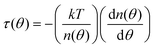 . Applying this equation to the data suffers from the typical problem that numerical differentiation of noisy data yields very noisy results. In the case of the data in Fig. 7, we can treat the NWs within the electrode gap as equivalent since the electric field does not vary within the gap region. On the other hand, each NW outside the gap is in a region of significantly different electric field. The number of counts for a NW outside the gap is further reduced by imposing a requirement that data be recorded only during the time the NW is in a small geographic region over which the electric fields do not vary substantially (Fig. 6B). Thus, there are sufficient counts for the NWs in the gap (panel A), but not for NW #18. Fig. 8 shows a numerical differentiation of the raw data from NWs in the gap. For small angles there are many data points, but as the angle approaches 0.1π, where the counts in Fig. 7A become small, the data become less reliable.
 | ||
| Fig. 8 Torques as a function of angle calculated from the data in Fig. 7A. The dashed line shows the expected functional form of the torque as a function of angle for the case of a NW in an electric field in the absence of other sources of torque. | ||
The size of the geographic region selected for NW #18 is somewhat arbitrary; we selected a region with a diameter of roughly the NW length, primarily because in most applications knowledge of torques on a smaller scale than the NW length is not necessary. A two-dimensional simulation of the electric fields in the absence of NWs predicts that the field direction will vary by about 0.1 radians (6 degrees) over this region (Fig. 6B), which is three bin-widths in the Fig. 7 histograms. Since there is a substrate and the NW itself modifies the local electric fields, the two-dimensional simulation is an approximation. Given the predicted curvature of the electric fields over the length of a NW it is a reasonable one. To get significantly higher accuracy a self-consistent three-dimensional simulation would also have to include the NWs' effect on the electric fields, and therefore would need to be performed for each NW position.28
The torque on a NW in a uniform electric field in the absence of other torques is expected to be a monotonically-increasing function of angle. As we have already discussed, the electric fields in these experiments are non-uniform on the length scales of the NWs, but this non-uniformity is small enough that the monotonicity of the torque as a function of angle should be maintained. The deviation in the measured torque in Fig. 8 from this simple behavior is consistent with the physical features of the sample. We used 100 nm of Au for the metal electrodes, which is a significant fraction of the NW diameter. The local maximum seen in Fig. 8 at around 0.05π is consistent with the NWs having rotated far enough that their ends fell between the electrodes. Thus, there was a physical barrier for them to climb in order to reduce their angle, which was manifested as a reduction in net torque in Fig. 8.
Further conclusions can be drawn about the DEP with some assumptions. For example, an energy analysis can be done using the angle data in Fig. 7. The simplest is a gauge of the depth of the potential well created by the DEP fields. The technique can thus be used to map out the potential landscape. The expected DEP torque for a NW in a uniform electric field is τ(θ) = 2gεmE2Cos(θ)Sin(θ), where g takes into account the polarizability of the NW and is related to the geometry of the NW and the imaginary part of the Clausius–Mossotti factor, εm is the permittivity of the medium,14,26,35 and θ is the angle relative to the electric field. In any DEP assembly of NWs where the NWs touch both electrodes, the electric fields cannot be uniform on the length scale of the NWs so this is a first-order approximation. Nevertheless, the functional form of the torque will be similar except for very inhomogeneous fields (i.e. those that make a large angle change within the length of the NW), so we use τ(θ) = 2·U·Cos(θ)Sin(θ) where U is the depth of the potential well. Integrating the torque equation and substituting into the Boltzmann distribution yields  . Fitting this equation to the data in Fig. 7 normalized by the number of samples gives the ratio U/kT (Fig. 7), the ratio between the potential well depth and the thermal energy.
Starting from the uniform-field approximation for U, U = gεmE2, we can map out the local electric field magnitude to a reasonable approximation by simply looking at the ratios of the potential well depth as a function of location. For example, by taking the ratios of the energy terms in Fig. 7, we can conclude that the electric field strength just a short distance outside the gap at the location of NW #18 is about 1/6 of the electric field strength within the gap (E2gap/E2NW#18 = 34), consistent with the two-dimensional simulations. With data collected for a sufficient period of time, this technique could map out electric field gradients in DEP experiments. Data such as this is very useful for the iterative design of electrodes. In the experiments reported here, we observed that most of the NWs in the gap at the end of the DEP initially fell out of suspension near or into the gap, and the few NWs which landed on the substrate outside the gap were attracted into the gap (as in Fig. 3). In order to increase the speed and efficiency of the process, it would be ideal to capture NWs from a wider range of the substrate. NW #18 was a few microns outside the gap and was very slowly attracted towards the gap during DEP. In order to improve the collection of NWs, we will modify the electrode design such that the electric fields over a much larger area are roughly 25% of the field strength in the gap, which will guide more NWs into the gap.
The technique presented for the torques is generalizable to other relevant forces on the NWs during assembly. For example, the next logical step is to extend the technique to measurements of lateral forces on NWs, which will include the forces that attract the NWs to the electrode gap and the repulsive forces between the NWs once they are in the gap. A first order estimate of these repulsive effects can be made by noting that the NWs are often found about 2 μm apart from each other, even when there is space to move laterally within the gap (Fig. 2). Therefore, for distances of greater than 2 μm, the repulsive forces are small compared to Brownian forces, otherwise the NWs would separate rapidly as they do when closer together than about 2 μm.
In summary, we have shown a method for controllable assembly and fixing of ordered parallel NW arrays and a quantitative tracking technique that allows high-accuracy quantitative positional mapping of the torques on the NWs, the potential well depths, and the local electric fields. From our analysis, U/kT of around 70 is ideal for aligning NWs without fixing them to the surface. This ratio provides guidance as to the optimal parameters for DEP-based assembly techniques. Thus, the described tracking technique and accompanying calculations enable intelligent refinement of DEP electrode geometries rather than a trial-and-error approach.
We thank the Defense Threat Reduction Agency and the National Consortium for Measurement and Signature Intelligence for financial support.
References
- C. R. Martin, Nanomaterials: A Membrane-Based Synthetic Approach, Science, 1994, 266, 1961 CrossRef CAS.
- A. Huczko, Template-based synthesis of nanomaterials, Appl. Phys. A: Mater. Sci. Process., 2000, 70, 365 CrossRef CAS.
- S. Park, S.-W. Chung and C. A. Mirkin, Hybrid Organic-Inorganic, Rod-Shaped Nanoresistors and Diodes, J. Am. Chem. Soc., 2004, 126, 11772 CrossRef CAS.
- M. T. Bjork, J. Knoch, H. Schmid, H. Riel and W. Riess, Silicon nanowire tunneling field-effect transistors, Appl. Phys. Lett., 2008, 92(19), 193504 CrossRef.
- K. Skinner, C. Dwyer and S. Washburn, Quantitative analysis of individual metal-CdSe-metal nanowire field-effect transistors, Appl. Phys. Lett., 2008, 92(11), 112105 CrossRef.
- L. Piraux, J. M. George, J. F. Despres, C. Leroy, E. Ferain, R. Legras, K. Ounadjela and A. Fert, Giant magnetoresistance in magnetic multilayered nanowires, Appl. Phys. Lett., 1994, 65(19), 2484 CrossRef CAS.
- A. Blondel, J. P. Meier, B. Doudin and J. P. Ansermet, Giant magnetoresistance of nanowires of multilayers, Appl. Phys. Lett., 1994, 65(23), 3019 CrossRef CAS.
- K. Liu, K. Nagodawithana, P. C. Searson and C. L. Chien, Perpendicular giant magnetoresistance of multilayered Co/Cu nanowires, Phys. Rev. B: Condens. Matter, 1995, 51(11), 7381 CrossRef CAS.
- A. Fert and L. Piraux, Magnetic nanowires, J. Magn. Magn. Mater., 1999, 200(1), 338 CrossRef CAS.
- J. K. N. Mbindyo, T. E. Mallouk, J. B. Mattzela, I. Kratochvilova, B. Razavi, T. N. Jackson and T. S. Mayer, Template synthesis of metal nanowires containing monolayer molecular junctions, J. Am. Chem. Soc., 2002, 124(15), 4020 CrossRef CAS.
- L. T. Cai, H. Skulason, J. G. Kushmerick, S. K. Pollack, J. Naciri, R. Shashidhar, D. L. Allara, T. E. Mallouk and T. S. Mayer, Nanowire-based molecular monolayer junctions: Synthesis, assembly, and electrical characterization, J. Phys. Chem. B, 2004, 108(9), 2827 CrossRef CAS.
- C. E. Gardner, M. A. Ghanem, J. W. Wilson and D. C. Smith, Development of a nanowire-based test bed device for molecular electronics applications, Anal. Chem., 2006, 78(3), 951 CrossRef CAS.
- L. Kim, J. Kim, G. H. Gu and J. S. Suh, Fabrication of well-ordered molecular device arrays, Chem. Phys. Lett., 2006, 427(1–3), 137 CrossRef.
- T. B. Jones, Electromechanics of Particles, Cambridge University Press, Cambridge, New York, 1995 Search PubMed.
- H. A. Pohl, Dielectrophoresis: The Behavior of Neutral Matter in Nonuniform Electric Fields, Cambridge University Press, Cambridge, New York, 1978 Search PubMed.
- P. A. Smith, C. D. Nordquist, T. N. Jackson, T. S. Mayer, B. R. Martin, J. Mbindyo and T. E. Mallouk, Electric-field assisted assembly and alignment of metallic nanowires, Appl. Phys. Lett., 2000, 77(9), 1399 CrossRef CAS.
- K. D. Hermanson, S. O. Lumsdon, J. P. Williams, E. W. Kaler and O. D. Velev, Dielectrophoretic assembly of electrically functional microwires from nanoparticle suspensions, Science, 2001, 294(5544), 1082 CrossRef.
- D. Aristides and A. Paschalis, One-, two-, and three-dimensional organization of colloidal particles using nonuniform alternating current electric fields, Electrophoresis, 2002, 23(14), 2174 CrossRef.
- K. H. Bhatt and O. D. Velev, Control and Modelling of the Dielectrophoretic Assembly of On-Chip Nanoparticle Wires, Langmuir, 2004, 20(2), 467 CrossRef CAS.
- S. Evoy, N. DiLello, V. Deshpande, A. Narayanan, H. Liu, M. Riegelman, B. R. Martin, B. Hailer, J. C. Bradley, W. Weiss, T. S. Mayer, Y. Gogotsi, H. H. Bau, T. E. Mallouk and S. Raman, Dielectrophoretic assembly and integration of nanowire devices with functional CMOS operating circuitry, Microelectron. Eng., 2004, 75, 31 CrossRef CAS.
- Y. J. Yuan, M. K. Andrews and B. K. Marlow, Chaining and dendrite formation of gold particles, Appl. Phys. Lett., 2004, 85(1), 130 CrossRef CAS.
- J. J. Boote and S. D. Evans, Dielectrophoretic manipulation and electrical characterization of gold nanowires, Nanotechnology, 2005, 16(9), 1500 CrossRef CAS.
- L. Dong, J. Bush, V. Chirayos, R. Solanki, J. Jiao, Y. Ono, J. F. Conley Jr and B. D. Ulrich, Dielectrophoretically controlled fabrication of single-crystal nickel silicide nanowire interconnects, Nano Lett., 2005, 5(10), 2112 CrossRef CAS.
- S. J. Papadakis, Z. Gu and D. H. Gracias, Dielectrophoretic assembly of reversible and irreversible metal nanowire networks and vertically aligned arrays, Appl. Phys. Lett., 2006, 88(23), 233118 CrossRef.
- K. Oh, J.-H. Chung, J. J. Riley, Y. Liu and W. K. Liu, Fluid flow-assisted dielectrophoretic assembly of nanowires, Langmuir, 2007, 23(23), 11932 CrossRef CAS.
- W. Ahmed, E. S. Kooij, A. van Silfhout and B. Poelsema, Quantitative Analysis of Gold Nanorod Alignment after Electric Field-Assisted Deposition, Nano Lett., 2009, 9(11), 3786 CrossRef CAS.
- R. Krupke, F. Hennrich, M. M. Kappes and H. V. Lohneysen, Surface conductance induced dielectrophoresis of semiconducting single-walled carbon nanotubes, Nano Lett., 2004, 4(8), 1395 CrossRef CAS.
- Y. L. Liu, J. H. Chung, W. K. Liu and R. S. Ruoff, Dielectrophoretic assembly of nanowires, J. Phys. Chem. B, 2006, 110(29), 14098 CrossRef CAS.
- S. Raychaudhuri, S. A. Dayeh, D. L. Wang and E. T. Yu, Precise Semiconductor Nanowire Placement Through Dielectrophoresis, Nano Lett., 2009, 9(6), 2260 CrossRef CAS.
- T. H. Kim, S. Y. Lee, N. K. Cho, H. K. Seong, H. J. Choi, S. W. Jung and S. K. Lee, Dielectrophoretic alignment of gallium nitride nanowires (GaN NWs) for use in device applications, Nanotechnology, 2006, 17(14), 3394 CrossRef CAS.
- E. M. Freer, O. Grachev, X. Duan, S. Martin and D. P. Stumbo, High-yield self-limiting single-nanowire assembly with dielectrophoresis, Nat. Nanotechnol., 2010, 5(7), 525 CrossRef CAS.
- H. Ye, Z. Gu, T. Yu and D. H. Gracias, Integrating nanowires with substrates using directed assembly and nanoscale soldering, IEEE Trans. Nanotechnol., 2006, 5(1), 62 CrossRef.
- Z. Gu, H. Ye and D. H. Gracias, The bonding of nanowire assemblies using adhesive and solder, JOM, 2005, 57(12), 60 CrossRef CAS.
- The particle tracking code is freely available from http://cismm.cs.unc.edu/downloads/. It is supported by the NIH NIBIB (NIH 5-P41-RR02170).
- B. M. I. van der Zande, G. J. M. Koper and H. N. W. Lekkerkerker, Alignment of Rod-Shaped Gold Particles by Electric Fields, J. Phys. Chem. B, 1999, 103(28), 5754 CrossRef CAS.
| This journal is © The Royal Society of Chemistry 2011 |